User Manuals: VIA Technologies EPIA-M920 Motherboard
Manuals and User Guides for VIA Technologies EPIA-M920 Motherboard. We have 4 VIA Technologies EPIA-M920 Motherboard manuals available for free PDF download: User Manual

VIA Technologies EPIA-M920 User Manual (93 pages)
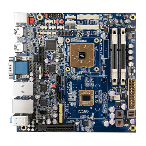
Highly-integrated low-power platform with rich feature set and multimedia capabilities
Brand: VIA Technologies
|
Category: Single board computers
|
Size: 6 MB
Table of Contents
-
-
-
-
HDMI ® Port20
-
PS/2 Port20
-
COM Port21
-
Audio Jack22
-
VGA Port22
-
USB 2.0 Port23
-
USB 3.0 Port23
-
Onboard I/O24
-
-
-
-
-
-
-
-
Control Keys56
-
Getting Help56
-
Main Menu57
-
-
-
-
Advertisement
VIA Technologies EPIA-M920 User Manual (82 pages)
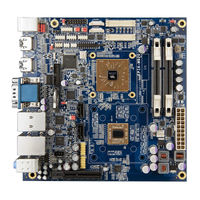
Highly-integrated low-power
platform with rich feature set
and multimedia capabilities
Brand: VIA Technologies
|
Category: Motherboard
|
Size: 3 MB
Table of Contents
-
-
-
-
HDMI ® Port21
-
PS/2 Port21
-
COM Port22
-
Audio Jack23
-
VGA Port23
-
USB 2.0 Port24
-
USB 3.0 Port24
-
-
-
-
-
-
-
-
-
Control Keys49
-
Getting Help49
-
Main Menu50
-
-
-

VIA Technologies EPIA-M920 User Manual (113 pages)
Brand: VIA Technologies
|
Category: Motherboard
|
Size: 3 MB
Table of Contents
-
-
-
PS/2 Port26
-
HDMI Port27
-
Audio Ports30
-
USB 2.0 Port32
-
USB 3.0 Port33
-
-
-
Jumpers58
-
Control Keys74
-
Getting Help75
-
Main Menu76
-
System Date77
-
System Time77
-
Panel Type93
-
Boot Settings101
-
Password Check104
-
Save Changes106
-
Discard Changes106
-
Advertisement

VIA Technologies EPIA-M920 User Manual (112 pages)
mini-itx embedded board
Brand: VIA Technologies
|
Category: Motherboard
|
Size: 3 MB
Table of Contents
-
-
-
PS/2 Port26
-
HDMI Port27
-
COM Port28
-
Audio Ports30
-
VGA Port31
-
USB 2.0 Port32
-
USB 3.0 Port33
-
-
-
Jumpers57
-
Control Keys71
-
Getting Help72
-
Main Menu73
-
System Date74
-
System Time74
-
Save Changes103
-
Discard Changes103
-
Advertisement
Related Products
- VIA Technologies EPIA-M900
- VIA Technologies EPIA-M910
- VIA Technologies EPIA-M920-10E
- VIA Technologies EPIA-M920-12Q
- VIA Technologies EPIA-M930
- VIA Technologies EPIA-ML8000AG - VIA Motherboard - Mini ITX
- VIA Technologies EPIA-M
- VIA Technologies EPIA-MII
- VIA Technologies EPIA Mini-ITX
- VIA Technologies EPIA-M830