Sign In
Upload
Manuals
Brands
NORCAL Manuals
Transceiver
NC2030
NORCAL NC2030 Manuals
Manuals and User Guides for NORCAL NC2030. We have
1
NORCAL NC2030 manual available for free PDF download: Manual
NORCAL NC2030 Manual (128 pages)
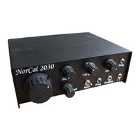
Low power, High Performance 20m or 30m DC Transceiver
Brand:
NORCAL
| Category:
Transceiver
| Size: 6.51 MB
Table of Contents
Table of Contents
2
A Bit of History and Recognition
8
Specifications
10
Receiver
10
Transmitter
10
Building the Kit
12
Things You will Need
12
Figure 1. Working over an Oversized Cookie Sheet Is Highly Recommended to Catch Stray Surface
13
Figure 2. a Temperature Controlled Soldering Helps a Lot. 650 to 700 Degrees Is Recommended
13
Figure 3. a very Pointed Soldering Iron Tip Is a very Big Help for Small Surface Mounted Components
13
Parts List
14
Figure 4. Headband Magnifiers. "Mag-Eyes" from Joann Fabrics
14
Figure 5. Parts in Bag Pockets Are Accessed Via Slit Cut into the Packet Just Larger Enough to Get the Part
15
Figure 6. Close up of a Surface Mount Parts Strip and the Bag Slit Just Large Enough to Access the Strip
15
Figure 7. a Sample Bag Pocket Layout Diagram Vs. a Real Bag of Parts
16
Figure 8. Layout of the Power Supply and the First Three Bags
17
Figure 9. Layout of Bags # 3 to # 6
18
Figure 10. Contents of Bags #7 - #9
19
Tools and Construction Hints
21
Power Supply
23
Figure 11. Completed Switching PS with Temporary 9V Power Connection and 100 Ohm 3.3V Dummy
23
Figure 12. Board Layout of the Switching Power Supply
23
Figure 13. Switching Supply Built up
24
Figure 14. Orientation of U1. Mount with the Markings "AANY" Upside down as Shown
24
Figure 15. PS with 0.1 Caps, 47 Uh Inductors, Schottky Diodes, and Switching IC
25
Figure 16. PS and Electrolytic Caps Polarity Details
25
Figure 17. L2 Mounting Details
26
Figure 18. L2 Details. after First 24 Turns, Add a Twisted Loop for Later Center Tap. Add 27 more Turns
27
Figure 19. Form 1N4001 Diode as Shown
27
Figure 20. 100 Ohm Temporary 3V Load Resistor Formed as Shown
27
Figure 21. 1N4001 Mounted and 9V Battery Clip Connected
28
Figure 22. 3V Temporary 100 Ohm Load Resistor Connected to Bottom of Board
28
Switching Regulator Tests
29
Figure 23. Power Output Connection Details (Load Resistor Not Shown)
29
Main Board Temporary Power Connections
30
Figure 24. Temporary 9V Power Connection and Connections between Switching Supply and Main Board
30
Main Board 3V and 5V Regulators
31
Figure 25. Close up of Power Connections on the Main Board and Switching Supply, Bypass Caps, and
31
Figure 26. Location of the Two 3V and 5V Regulator Sections
31
Figure 27. Close up of First Two 3V LDO Regulators
32
Figure 28. Parts Layout of First Two 2.9V LDO Regulators. Note the Black Band Orientation of the
32
Figure 29. Location of the One 3V and Two 5V LDO Regulator Sections
33
Figure 30. Installed Parts for this Section of LDO Regulators. Note the Black Band Orientation on the
34
3V and 5V LDO Regulator Tests
35
Figure 31. Ground Reference for Voltage Measurements Are Upper 2 Corners, the Lower 2 Are Not
35
HPF, Audio Amp, Mute, Audio Limiter and Headphone Drivers
37
Figure 32. SCAF, HPF, Audio Amp, and Headphone Driver Section of the Board
37
Figure 33. HPF, Audio Amp, Headphone Drivers Portion
37
Figure 34. Picture Shows Orientation of U11 with Stripe on Upper End
38
Audio Section Partial Tests
39
SCAF Variable Low Pass Filter
39
Figure 35. General Location of the SCAF Circuit
39
Figure 36. Close up Component View of the SCAF Section of the Board
39
SCAF and Additional Audio Section Tests
40
Figure 37. U13 and D10 Mounted. IC Notch and D10 Flat Side in the Vertical Direction
40
CW Keyer
42
Figure 38. Location of the CW Keyer Section of the Board
42
Figure 39. Close up of the CW Keyer Section
42
Figure 40. Picture Showing Correct Orientation of Norcal Keyer Chip (Optional Socket Not Shown)
43
Audio Frequency Annunciator
44
Figure 41. General Location of AFA Circuit
44
Figure 42. Close up View of the AFA Section
44
Adding External Controls for Functionality Tests
45
Figure 43. Correct Orientation of both the 8 Pin 12C508 AFA Chip and 14 Pin 74ACT00 Ics
45
Figure 44. Connect Buttons Keyer and AFA Buttons S2 and S3 as Shown
46
Figure 45. Prepare R88 100K Cw Speed Pot as Shown. the Left and Middle Terminals Are Connected to
47
Figure 46. Connect R88 CW Speed Pot to the R88 Pads as Shown. Keep Black and White in Order Shown
47
Figure 47. Use Brown/Red/Orange Wire and Connect up the Paddle Jack in the Color Order Shown
47
Figure 48. Attach Paddle Jack to JP5 Using the Color Order Shown
48
Figure 49. Use Brown/Red/Orange Wire and Connect up the Headphone Jack in the Color Order Shown
48
Figure 50. Connect the Headphone Jack to JP4 in the Color Order Shown
48
Figure 51. Use Yellow/Green/Blue Wire to Connect to R83, the 50K SCAF Pot in the Color Order Shown
49
Figure 52. Connect the 50K SCAF Pot to the R83 Header Pads in the Color Order Shown
49
Figure 53. Use Yellow/Green/Blue Wire to Connect to R77, the 5K Volume Control Pot in the Color Order
49
Figure 54. Connect the 5K Volume Control Pot to the R77 Header Pads in the Color Order Shown
50
Figure 55. All Controls Attached Thus Far
50
Keyer, AFA and Additional Audio Section Tests
51
VXO and T/R Offset
52
Figure 56. Location of VXO and T/R Offset Circuit
52
Figure 57. Close up of VXO and T/R Offset Circuit
52
Figure 58. Proper Orientation of U8, D2, and D3
53
Figure 59. Yellow/Green/Blue Wire to Connect to R52, the 25K RIT Pot in the Color Order Shown
54
Figure 60. Connect the 25K RIT Pot to the R52 Header in the Color Order Shown. also Attach a SPDT
54
AFA RF Buffer and Phase Splitter
55
Figure 61. General Location of the AFA RF Buffer and Phase Splitter
55
Figure 62. Close up View of the AFA RF Buffer and Phase Splitter Area
55
Band Specific Parts
56
Figure 63. Orientation of U9 Labeling as Installed
56
VXO and AFA Buffer Tests
57
Figure 64. Temporary Connection from C72 to C54
57
LO Mixer and PTO
59
Figure 65. Board Location of the lo Mixer and PTO Circuitry
59
Figure 66. Close up of the PTO and Mixer Section of the Board
59
Figure 67. PTO and PTO/VXO Mixer Sections as Built
60
Figure 68. Temporary Soda Straw PTO Coil L13 Connected to the PTO Oscillator Circuit
61
Figure 69. Anchoring the First Turn of the Temporary PTO Coil
62
Figure 70. Finished Temporary PTO Coil with 82T. Tie off Holes Placed on both Ends
62
Figure 71. Mcdonald's Straw Diameter
63
Figure 72. Main Tuning PTO Coil L13 Shown Mounted to the Front Panel. this Is Used Only When the Rig
63
Figure 73. Wrap First Turn on the PTO Coil. Position ¾" Back from Front, Twist Single Turn in Place
64
Figure 74. First Turn Is Glued (Epoxy) into Place to Make It Easier to Wrap the Rest of the Turns
64
Figure 75. Coil with Completed 105 Turns. Turns Wound Tight and "Shoulder to Shoulder
65
Figure 76. PTO Coil Coated in Clear Nail Polish. the Wife Recommends "Sally Hansen Diamond
65
Figure 77. 2" Brass Screw Cut Back to a Total Length of 1 ¾ Inches
66
Figure 78. Final Screw with Mounted Spacer
66
LO Filter and lo Amp
67
Figure 79. General Location of lo Filter and Amp
67
Figure 80. Close up of the lo Filter and Amp Components
67
Figure 81. lo Filter and Amplifier as Built. both Trim Caps Must Have Proper Orientation
68
Figure 82. Coils L6 and L7 Are Prepared to be Mounted Surface Mount Style on the Top of the Board on
68
First Time lo Filter Tune up
69
Quadrature Detector/Front End Filter
70
Figure 83. General Location of the Detector and Front End Filter
70
Figure 84. Close up of the Detector and the RF Tuned Front End
70
Figure 85. Picture of Detector and RF Front End with Parts Installed. Note Trim Cap Orientation and Jumper on JP3
71
Figure 86. Detail on T1. Two Turn # 32 to Pads 1 & 2. Main Winding Connect to Pads 3 & 4
72
Figure 87. L2 Leads Formed to Prepare for Surface Mounting on the Top of the through Hole Pads
72
Detector Tests
73
Audio Pre-Amp and Audio Phasing
74
Figure 88. Location of Audio Preamp and Phasing Sections
74
Figure 89. Close up of Audio Preamp and Phasing Sections
74
Figure 90. Component Alignment of U4, and U5. Note C30, R22 Locations
75
Audio Pre-Amp and Audio Phasing Tests
76
Main Audio Filter
76
Figure 91. General Location of the Audio 750 Hz LPF
76
Figure 92. Close up of the 750 Hz Audio LPF Section
77
Figure 93. Component Placement and Alignment of U7 and Polarization of Caps C47, C48, C49
77
Main Audio Filter Tests
78
Transmitter
79
Figure 94. General Location of the Transmitter Section
79
Figure 95. Close up of the Transmitter Section Portion
79
Figure 96. All Transmitter Parts Except for the Inductors. Note TS912 Orientation, BS170 Flat Side
80
Figure 97. L19 Mounted. 3T Tap Location Shown
81
Transmitter Tests
82
Figure 98. Location of U9 and Pins Voltages to Check. in Receive Mode, Check, U9 Pins 11 (0V), 12 &13
82
Figure 99. Location of U15 between AFA and Keyer Chips. Test Pins 11, 12, and 13
83
Figure 100. Location of R95 and R96. Voltages on Transmit/Receive Switches
84
Mounting into the Case
85
Bolt down the PC Board
85
Add Front Panel Hardware
85
Figure 101. Mount All Four Corners of the Main Board Using the Mounting Hardware as Shown
85
Figure 102. NC2030 with All Front Panel Hardware Mounted in Prototype Chassis. Case will be Silk
85
Figure 103. Mount the Paddle Jack
86
Figure 104. Mount the Headphone Jack
86
Figure 105. Add Keyer Button (Upper Left), AFA Button (Lower Right)
87
Figure 106. Mount the Volume Control Pot (Upper Right) and the Spot Switch (Lower Middle)
87
Figure 107. Another View of the Spot Switch. the Two Terminals Are Orientated in the "Up" Position
88
Figure 108. Add Keyer Speed Pot, SCAF Pot, and RIT Pot
88
Add Rear Panel Hardware
89
Figure 109. Rear Panel of Prototype NC2030. Final Case will be Silk Screened
89
Figure 110. Antenna Jack Added
89
Figure 111. Rear Power Connections: Power Switch, Leads to Rear Switching Supply, Power Jack
90
Figure 112. Power Jack Connections, +12V to Power Switch (Red Wire) and Ground (Green) to JP2 Ground
90
Figure 113. Placement of the Switching Supply Tin on the Back Chassis, Power Jack Not Installed
91
Figure 114. Place the Switching Supply Board in the Tin, Center It Top & Bottom, and Mark the Mounting
92
Figure 115. Connect the Power Wires to the Switching Supply in the Color Order Shown
93
Figure 116. PTO L13 Mounting Detail. Coil Connections Shown. Front PTO Coil Wire Must Connect as
93
Figure 117. Connections for the PTO Coil L13
94
Figure 118. Front Side of the PTO Coil (Prototype Chassis) Showing Epoxy Ridge from the Front Side
94
Figure 119. Tuning Knob with PTO Screw Partially Inserted
95
Figure 120. PTO Brass Screw Full Inserted into the PTO Coil
95
Receiver Alignment Section
96
LO Filter Tune up
96
Figure 121. with PTO Screw Fully Inserted, Adjust Tuning Knob to Have a Small Amount of Front Panel
96
Figure 122. Location of lo Trim Caps C58, C60 and TP3 in the Upper Left Corner of the Board
96
PTO Frequency Alignment
97
PTO Tuning for the 20M Version (2.941 to 3.006 Mhz)
97
Figure 123. L13 PTO Tuning Coil as Mounted. Remove Turns off the End Simply by Pulling on the Wire
97
PTO Tuning for the 30M Version (2.850 to 2.900 Mhz)
98
Mixer/Lo Amp Gain Selection
98
Figure 124. Location of R63, PTO/VXO Mixer Gain Adjust Located in Bottom Left Corner of Board
99
RF Front End Tune up
100
Figure 125. Location of Optional lo Amplifier Gain Adjust Resistor R50
100
Figure 126. Location of RF Front End Band Pass Filter Adjust Trim Caps, C23 and C25 on Top Middle of
100
Opposite Sideband Suppression
102
Figure 127. Adjustment Points for Nulling out the Opposite Sideband
102
Figure 128. Picture of Simulated Opposite Sideband Rejection When Optimally Tuned up
103
Setting RX/TX Offset
104
Figure 129. Location of the T/R Offset Trim Pot, R53
105
Transmitter Test
106
Operating the NC2030
106
Principles of Operation
109
Transceiver Block Diagram
109
Receiver
109
T/R Switch
109
Detector/ AF Pre-Amp
110
Figure 130. Tayloe Quadrature Detector and I/Q Audio Preamplifier Schematic
110
Phasing Strip
113
Figure 131. Audio Phasing Section Schematic
113
R/C Audio Filter - Low Pass
114
Figure 132. Main Brick Wall Filter. 800 Hz Active R/C Low Pass Filter
114
R/C Audio Filter - High Pass
115
Figure 133. 400 Hz High Pass Filter Schematic
115
Audio Amplifier, Mute Switch & Audio Limiter
116
SCAF Variable Low Pass Filter & Headphone Drivers
117
Figure 134. SCAF Low Pass Filter and Headphone Amplifier
117
PTO Circuit
118
VXO Circuit (20M - 11.059 Mhz, 30M - 13.0 Mhz)
118
Figure 135. PTO Schematic
118
Figure 136. VXO Schematic and Transmit/Receive Offset Switching
118
LO Mixer and if Filter
120
LO if Amp and Phase Splitter
120
Figure 137. lo Mixer and if Filter Schematic
120
Figure 138. Schematic of lo Amplifier and Detector Clock Phase Splitter
120
Transmitter
121
Class E PA Finals
121
Figure 139. Schematic of Class E Transmitter
121
CW Waveform Shaping
122
High Voltage/High Current PA Protection
122
AFA Frequency Counter Instructions
122
Introduction
122
Counter Modes
122
Mode
123
Digits Announced
123
Counter Usage
123
Keyer Instructions
124
Out
124
Figure 140. a Function Table of the Keypress Combinations
124
Figure 141. Mem + Dit Menu (PAR Mem to Advance to the Next Menu Item)
125
Figure 142. Mem + Dah Menu (PAR Mem to Exit)
126
Figure 143. Mem Switch Menu (PAR Mem to Advance to the Next Menu Item)
127
Figure 144. Mem + both Menu (PAR Mem to Exit)
127
Advertisement
Advertisement
Related Products
NORCAL 2N2/XX
NORCAL Categories
Transceiver
More NORCAL Manuals
Login
Sign In
OR
Sign in with Facebook
Sign in with Google
Upload manual
Upload from disk
Upload from URL