Table of Contents
Advertisement
SERVICE MANUAL
Main Section
I Specifications
I Preparation for Servicing
I Adjustment Procedures
I Schematic Diagrams
I CBA
I Exploded Views
I Parts List
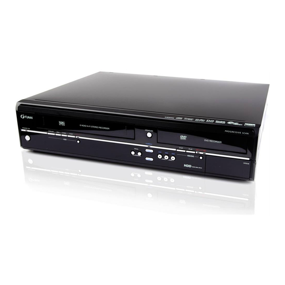
VIDEO CASSETTE RECORDER
HDD & DVD /
TD6D-M101
When servicing the deck
mechanism, refer to MK14 Deck
Mechanism Section.
Deck Mechanism Part No.:
N25E1FL
Advertisement
Table of Contents

Subscribe to Our Youtube Channel
Related Manuals for FUNAI TD6D-M101


Summary of Contents for FUNAI TD6D-M101
- Page 1 I Specifications mechanism, refer to MK14 Deck I Preparation for Servicing Mechanism Section. I Adjustment Procedures I Schematic Diagrams Deck Mechanism Part No.: I CBA I Exploded Views N25E1FL I Parts List HDD & DVD / VIDEO CASSETTE RECORDER TD6D-M101...
-
Page 2: Table Of Contents
MAIN SECTION HDD & DVD / VIDEO CASSETTE RECORDER TD6D-M101 Main Section I Specifications I Preparation for Servicing I Adjustment Procedures I Schematic Diagrams I CBA I Exploded Views I Parts List TABLE OF CONTENTS Specifications ................1-1-1 Laser Beam Safety Precautions. -
Page 3: Specifications
SPECIFICATIONS General VCR video heads Four heads Internal 2.5 inch HDD 500 GB Power requirements 220–240 V ± 10 %, 50 Hz ± 0.5 % Power consumption 48 W Power consumption (standby) 0.5 W (When “Antenna Out” is set to “OFF”) Weight 5.4 kg Dimensions (width x height x depth) -
Page 4: Laser Beam Safety Precautions
LASER BEAM SAFETY PRECAUTIONS This DVD player uses a pickup that emits a laser beam. Do not look directly at the laser beam coming from the pickup or allow it to strike against your skin. The laser beam is emitted from the location shown in the figure. When checking the laser diode, be sure to keep your eyes at least 30 cm away from the pickup lens when the diode is turned on. -
Page 5: Important Safety Precautions
IMPORTANT SAFETY PRECAUTIONS Product Safety Notice K. When connecting or disconnecting the internal connectors, first, disconnect the AC plug from the Some electrical and mechanical parts have special AC outlet. safety-related characteristics which are often not L. Be sure to confirm the FAN motor has completely evident from visual inspection, nor can the protection stopped when disconnecting the AC cord for they give necessarily be obtained by replacing them... - Page 6 Safety Check after Servicing Examine the area surrounding the repaired location for damage or deterioration. Observe that screws, parts, and wires have been returned to their original positions. Afterwards, do the following tests and confirm the Chassis or Secondary Conductor specified values to verify compliance with safety standards.
-
Page 7: Standard Notes For Servicing
STANDARD NOTES FOR SERVICING Circuit Board Indications Pb (Lead) Free Solder 1. The output pin of the 3 pin Regulator ICs is When soldering, be sure to use the Pb free solder. indicated as shown. How to Remove / Install Flat Pack-IC Top View Bottom View 1. - Page 8 3. The flat pack-IC on the CBA is affixed with glue, so With Soldering Iron: be careful not to break or damage the foil of each 1. Using desoldering braid, remove the solder from pin or the solder lands under the IC when all pins of the flat pack-IC.
- Page 9 With Iron Wire: 2. Installation 1. Using desoldering braid, remove the solder from 1. Using desoldering braid, remove the solder from all pins of the flat pack-IC. When you use solder the foil of each pin of the flat pack-IC on the CBA flux which is applied to all pins of the flat pack-IC, so you can install a replacement flat pack-IC more you can remove it easily.
- Page 10 Instructions for Handling Semi- conductors Electrostatic breakdown of the semi-conductors may occur due to a potential difference caused by electrostatic charge during unpacking or repair work. 1. Ground for Human Body Be sure to wear a grounding band (1 MΩ) that is properly grounded to remove any static electricity that may be charged on the body.
-
Page 11: Handling Precautions For Hdd
HANDLING PRECAUTIONS FOR HDD CAUTION: 4. OTHERS a. Be careful so as not to do the followings. 1. SHOCK Otherwise, HDD might be damaged. a. Exposing HDD to shock may be the biggest - DO NOT disassemble HDD. damaging factor. Please note that HDD is easily - When handling HDD, be sure to hold both sides damaged even if dropped from any height. -
Page 12: Preparation For Servicing
PREPARATION FOR SERVICING How to Enter the Service Mode About Optical Sensors Caution: An optical sensor system is used for the Tape Start and End Sensors on this equipment. Carefully read and follow the instructions below. Otherwise the unit may operate erratically. What to do for preparation Insert a tape into the Deck Mechanism Assembly and press [ B ] (VCR) button. -
Page 13: Cabinet Disassembly Instructions
CABINET DISASSEMBLY INSTRUCTIONS 1. Disassembly Flowchart Fig. Loc. Part Removal Note This flowchart indicates the disassembly steps to gain access to items to be serviced. When reassembling, 2(S-10), (S-11), follow the steps in reverse order. Bend, route, and Assembly CN5002 dress the cables as they were originally. - Page 14 Note: (1): Identification (location) No. of parts in the figures (S-1) [1] Top Cover (2): Name of the part (3): Figure Number for reference (S-1) (S-1) (4): Identification of parts to be removed, unhooked, unlocked, released, unplugged, unclamped, or desoldered. P=Spring, L=Locking Tab, S=Screw, CN=Connector e.g.
- Page 15 [11] Motor [6] HDD Assembly (S-11) [12] Rear Panel DC Fan Mecha Earth (S-13) (S-15) (S-7) Plate CN5002 (S-17) CN652 CN981 (S-16) CN502 Rear Holder CN701 CN101 (S-9) (S-14) (S-7) CN901 [10] Fan Holder (S-17) [5] *DVD (S-8) Mechanism CN1002 &...
- Page 16 (S-25) (S-24) [18] VCR Chassis Unit [17] Power SW (S-23) Desolder Lead with blue stripe Fig. D7 1-7-4 E3TFGDC...
- Page 17 Cylinder Assembly FE Head ACE Head Assembly [19] Deck SW507 Assembly LD-SW [21] Rear Jack [20] DTV Module CBA Unit [22] AV CBA [19] Deck Assembly Cam Gear Hole Shaft Hole (S-26) LD-SW [22] AV CBA [22] AV CBA (S-27) Desolder Desolder From...
- Page 18 (S-28) [23] Deck Pedestal [25] Bracket R (S-31) [24] Front Bracket R DV Earth Plate (S-29) (S-30) DV Cable Fig. D9 1-7-6 E3TFGDC...
- Page 19 3. How to Eject Manually Note: When rotating the gear, be careful not to damage the gear. 1. Remove the Top Cover, Front Assembly, Front Bracket, DVD Mechanism & DVD/HDD Main CBA Assembly. 2. Remove the Dust Cover. 3. Rotate the gear in the direction of the arrow manually as shown below the tray descends. 4.
-
Page 20: Electrical Adjustment Instructions
ELECTRICAL ADJUSTMENT INSTRUCTIONS Head Switching Position Adjustment Note: 1. Electrical adjustments are required after replacing Purpose: circuit components and certain mechanical parts. To determine the Head Switching position during It is important to do these adjustments only after playback. all repairs and replacements have been completed. -
Page 21: How To Self-Check And Hdd Format
HOW TO SELF-CHECK AND HDD FORMAT 1. Turn on the HDD & DVD/VCR. 2. To put the HDD & DVD/VCR into the HDD mode, press [HDD] on the remote control unit. 3. To put the HDD & DVD/VCR into the self-check mode, after pressing [VARIABLE SKIP] button, press the [0], [7], and [9] buttons on the remote control in that order within three seconds. - Page 22 Table 2: Indication of DVD self-check (*4) INDICATION DESCRIPTION Connection of DVD is normal. NOT FOUND DVD drive cannot be found. FFC cable (connecting to CN201 & CN301) between the DVD drive and the DVD/HDD Main CABLE ERROR CBA is not connected correctly. Table 3: Indication of HDD self-check (*5) INDICATION DESCRIPTION...
-
Page 23: How To Initialize The Hdd & Dvd/Vcr
HOW TO INITIALIZE THE HDD & DVD/VCR To put the program back at the factory-default, initialize the HDD & DVD/VCR as the following procedure. < HDD/DVD Section > 1. Turn on the HDD & DVD/VCR. 2. To put the HDD & DVD/VCR into the HDD mode, press [HDD] on the remote control unit. -
Page 24: Firmware Renewal Mode
FIRMWARE RENEWAL MODE 1. Turn the power on and remove the disc in the tray. 5. Select the firmware version pressing arrow buttons, then press [ENTER/OK]. 2. To put the HDD & DVD into the HDD mode, press Fig. d appears on the screen and Fig. e appears [HDD] on the remote control unit. - Page 25 How to Verify the Firmware Version 1. Turn the power on. 2. To put the HDD & DVD into HDD mode, press [HDD] on the remote control unit. 3. To put the HDD & DVD into version display mode, press [VARIABLE SKIP], [1], [2], and [3] buttons on the remote control unit in this order within three seconds.
-
Page 26: Function Indicator Symbols
FUNCTION INDICATOR SYMBOLS < VCR Section > Note: If a mechanical malfunction occurs, the power is turned off. Turn the power back on by pressing [STANDBY- ON] button and an error message will be displayed on the TV screen for 5 seconds MODE INDICATOR ACTIVE When reel or capstan mechanism is not... - Page 27 < DVD Section > Note: If an error occurs, a message with the error number appears on the screen. Recording Error Error message You cannot record on this disc as Power Calibration Area is full. Error No. Error Message Solution Error Description An error occurs during data reading.
- Page 28 Error Message Solution Error Description Disc is full. Insert the recordable disc with No available recording space. (No area for new recording) enough recording space. The 99 title limit has been reached. You cannot record more than (Video Format Disc) 99 titles on one disc.
-
Page 29: Troubleshooting
TROUBLESHOOTING 1 Power Supply Section FLOW CHART NO.1 The power cannot be turned on. See FLOW CHART No.2 <The fuse blows out.> Is the fuse (F1001) normal? Is normal state restored when once unplugged power Check for leak or short-circuiting of primary circuit cord is plugged again after several seconds? component and service it if defective. - Page 30 FLOW CHART NO.6 AL+44V is not outputted. Check D013, D1140 and their periphery, and service it Is the supply voltage 44V fed to the cathode of D013? if defective. Check for short-circuiting or leak on the load circuit, and service it if defective. FLOW CHART NO.7 TU+30V is not outputted.
- Page 31 FLOW CHART NO.11 AL+5V is not outputted. Is the supply voltage 5V fed to the cathode of D016? Check D016, D1102 and their periphery, and service if defective. Check for short-circuiting or leak on the load circuit, and service it if defective. FLOW CHART NO.12 P-ON+5V(VCR) is not outputted.
- Page 32 FLOW CHART NO.15 DVD-P-ON+5V is not outputted. Is the supply voltage 5V fed to the cathode of D016? Check D016, D1102 and their periphery, and service it if defective. Is the "H" pulse (approximately 6V) inputted to Refer to "FLOW CHART NO.16"<P-ON+10V is not the base of Q1106? outputted>.
- Page 33 FLOW CHART NO.19 P-ON+1.8V is not outputted. Is 2.5V voltage supplied to pin(1) of IC1103? Check D1033 and their periphery, and service it if defective. Is the "H" pulse (approximately 5V) inputted to Check the REG-CONT signal line, and service it if the base of Q1109? defective.
- Page 34 2 HDD/DVD Section FLOW CHART NO.1 The key operation is not functioning. Are the contact point and the installation state of Re-install the key switches correctly or replace the defective key switches. the key switches normal? Check the key switches and their periphery, and service Is the control voltage normally inputted into Pin(8) of IC501? it if defective.
- Page 35 FLOW CHART NO.3 No HDD operation is possible from the remote control or the unit. Reconnect the FFC cable or wires. Are the FFC cable or wires connected properly? Check Q1100 and their periphery, and service it if Is 12V voltage supplied to Pin(20, 21, 22) of CN5003? defective.
- Page 36 Are the video signals outputted to each pin of CN1502? Replace DVD MECHANISM & DVD/HDD MAIN CBA ASSEMBLY. CN1502 7PIN VIDEO-Y(I/P)-OUT CN1502 1PIN VIDEO-Y(I)-OUT CN1502 5PIN VIDEO-Pr/Cr-OUT CN1502 3PIN VIDEO-Pb/Cb-OUT CN1502 9PIN VIDEO-C-OUT Are the video signals shown above inputted into each Check the line between each pin of CN1502 and pin of IC1509? each pin of IC1509, and service it if defective.
- Page 37 FLOW CHART NO.6 Picture does not appear normally. Set the disc on the disc tray, and playback it. (DVD MODE) Or, playback by selecting the picture in HDD top menu. (HDD MODE) Replace DVD MECHANISM & DVD/HDD MAIN CBA Are the video signals outputted to each pin of CN1502? ASSEMBLY.
- Page 38 FLOW CHART NO.7 Audio E-E does not appear normally. Check the line between audio input terminal and Are the audio signals inputted to each pin of IC1509? each pin of IC1509, and service it if defective. → IC1509 84,85PIN AUDIO-IN1 (AV1) IC1509 84,85PIN JK1504...
- Page 39 Replace DVD MECHANISM & DVD/HDD MAIN CBA Are the analog audio signals outputted to each pin of ASSEMBLY. CN1502? CN1502 17PIN AUDIO (L)-OUT CN1502 15PIN AUDIO (R)-OUT Are the analog audio signals inputted to each pin of Check each line between each pin of CN1502 and each IC1509? pin of IC1509, and service it if defective.
- Page 40 FLOW CHART NO.8 Audio is not outputted during playback. Set the disc on the disc tray, and playback it. (DVD MODE) Or, playback by selecting the picture in HDD top menu. (HDD MODE) Replace DVD MECHANISM & DVD/HDD MAIN CBA Are the analog audio signals outputted to each pin of ASSEMBLY.
- Page 41 3 VCR Section FLOW CHART NO.1 The key operation is not functioning. Are the contact point and the installation state of the Re-install the key switches correctly or replace key switches normal? the defective key switches. Check the key switches and their periphery, and service Is the control voltage normally inputted into Pin(7) of it if defective.
- Page 42 FLOW CHART NO.3 Cassette tape can not be loaded. Check the line between the start sensor and Pin(100) When loading a cassette tape, on Pin(100) of IC501, of IC501, and service it if defective. does the "L" pulse switch to the "H" pulse? When loading a cassette tape, is the specified voltage Replace the Capstan Motor Unit.
- Page 43 FLOW CHART NO.6 Capstan Motor does not rotate. Is 5V voltage supplied to Pin(2) of CN502? Check the P-ON+5V line and service it if defective. Is over approximately 2.6V voltage supplied to Pin(5) Check the line between Pin(5) of CN502 and Pin(76) of of CN502? IC501, and service it if defective.
- Page 44 FLOW CHART NO.10 Video E-E does not appear normally. Are the video signals inputted to each pin of IC1509? Check the line between video input terminal and each pin of IC1509, and service it if defective. IC1509 20PIN VIDEO-IN 1 (AV1) →...
- Page 45 FLOW CHART NO.11 Hi-Fi E-E audio does not operate normally. Check the line between audio input terminal and each pin of IC1509, and service it if defective. Are the audio signals inputted to each pin of IC1509? → IC1509 84,85PIN JK1504 AUDIO-IN1 (AV1) IC1509...
- Page 46 FLOW CHART NO.12 Hi-Fi audio can not be recorded normally. (E-E mode is normal.) Replace IC451. Is the Hi-Fi-COM signal outputted to Pin(26) of IC451? Check the line between Pin(8) of CN251 and Pin(26) Is the line between Pin(8) of CN251 and Pin(26) of IC451 normal? of IC451, and service it if defective.
- Page 47 FLOW CHART NO.15 Audio can not be playbacked normally in the linear audio mode. (E-E mode is normal.) Is the audio signal outputted to Pin(11) of IC301? Is the audio signal supplied to Pin(5) of IC301? Replace IC301. Check the line between Pin(11) of IC301 and Pin(80) of IC451, and service it if defective.
-
Page 48: Block Diagrams
BLOCK DIAGRAMS Servo/System Control Block Diagram 1-14-1 E3TFGBLS... - Page 49 Sub System Control Block Diagram E3TFGBLSS 1-14-2...
- Page 50 Digital Signal Process Block Diagram 1-14-3 E3TFGBLD...
-
Page 51: Video Selector Block Diagram
Video Selector Block Diagram E3TFGBLVS 1-14-4... -
Page 52: Video Block Diagram
Video Block Diagram TMDS TRANSMITTER TMDS ENCODER HDCP CIPHER/ ENCRYPTOR CONTROLLER AUDIO TO DIGITAL SIGNAL PROCESS BLOCK DIAGRAM 1-14-5 E3TFGBLV... - Page 53 Audio Selector Block Diagram E3TFGBLAS 1-14-6...
- Page 54 Audio Block Diagram E3TFGBLA 1-14-7...
- Page 55 Hi-Fi Audio Block Diagram 1-14-8 E3TFGBLH...
- Page 56 Power Supply Block Diagram 1-14-9 E3TFGBLP...
- Page 57 Sub Power Supply Block Diagram 1-14-10 E3TFGBLSP...
- Page 58 DTV Module Block Diagram 1-14-11 E3TFGBLDTV...
-
Page 59: Schematic Diagrams / Cba And Test Points
SCHEMATIC DIAGRAMS / CBA AND TEST POINTS Standard Notes WARNING Many electrical and mechanical parts in this chassis have special characteristics. These characteristics often pass unnoticed and the protection afforded by them cannot necessarily be obtained by using replacement components rated for higher voltage, wattage, etc. - Page 60 LIST OF CAUTION, NOTES, AND SYMBOLS USED IN THE SCHEMATIC DIAGRAMS ON THE FOLLOWING PAGES: 1. CAUTION: FOR CONTINUED PROTECTION AGAINST FIRE HAZARD, REPLACE ONLY WITH THE SAME TYPE FUSE. 2. CAUTION: Fixed Voltage (or Auto voltage selectable) power supply circuit is used in this unit. If Main Fuse (F1001) is blown, first check to see that all components in the power supply circuit are not defective before you connect the AC plug to the AC power supply.
- Page 61 AV 1/10 Schematic Diagram < VCR Section > 1-15-3 E3TFGSCAV1...
- Page 62 AV 2/9, Power SW & Sensor Schematic Diagram < VCR Section > FL601 MATRIX CHART BS CS DR DTV BS CS 1-15-4 E3TFGSCAV2...
- Page 63 AV 3/10 Schematic Diagram < VCR Section > 1-15-5 E3TFGSCAV3...
- Page 64 AV 4/10 Schematic Diagram < VCR Section > 1-15-6 E3TFGSCAV4...
- Page 65 AV 5/10 Schematic Diagram < VCR Section > 1-15-7 E3TFGSCAV5...
- Page 66 AV 6/10 Schematic Diagram < VCR Section > 1-15-8 E3TFGSCAV6...
- Page 67 AV 7/10 Schematic Diagram < VCR Section > 1-15-9 E3TFGSCAV7...
- Page 68 AV 8/10 Schematic Diagram < VCR Section > E3TFGSCAV8 1-15-10...
- Page 69 AV 9/10 Schematic Diagram < VCR Section > E3TFGSCAV9 1-15-11...
- Page 70 AV 10/10 Schematic Diagram < VCR Section > E3TFGSCAV10 1-15-12...
- Page 71 Power Supply Schematic Diagram < VCR Section > CAUTION ! CAUTION ! NOTE: Fixed voltage (or Auto voltage selectable) power supply circuit is used in this unit. For continued protection against fire hazard, The voltage for parts in hot circuit is measured using If Main Fuse (F1001) is blown , check to see that all components in the power supply replace only with the same type fuse.
- Page 72 Function, SW & USB Schematic Diagram < VCR Section > CAUTION ! For continued protection against fire hazard, replace only with the same type fuse(F6001). NOTE: Either IC3607 or IC3608 is used for FUNCTION CBA. E3TFGSCF 1-15-14...
- Page 73 Rear Jack Schematic Diagram < VCR Section > 1-15-15 E3TFGSCRJ...
- Page 74 DVD/HDD Main 1/7 Schematic Diagram < DVD/HDD Section > 1 NOTE: The order of pins shown in this diagram is different from that of actual IC101. IC101 is divided into six and shown as IC101 (1/6) ~ IC101 (6/6) in this DVD/HDD Main Schematic Diagram Section. 1-15-16 E3TFGSCD1...
- Page 75 DVD/HDD Main 2/7 Schematic Diagram < DVD/HDD Section > 1 NOTE: The order of pins shown in this diagram is different from that of actual IC101. IC101 is divided into six and shown as IC101 (1/6) ~ IC101 (6/6) in this DVD/HDD Main Schematic Diagram Section. 1-15-17 E3TFGSCD2...
- Page 76 DVD/HDD Main 3/7 Schematic Diagram < DVD/HDD Section > 1 NOTE: The order of pins shown in this diagram is different from that of actual IC101. IC101 is divided into six and shown as IC101 (1/6) ~ IC101 (6/6) in this DVD/HDD Main Schematic Diagram Section. 1-15-18 E3TFGSCD3...
- Page 77 DVD/HDD Main 4/7 Schematic Diagram < DVD/HDD Section > 1 NOTE: The order of pins shown in this diagram is different from that of actual IC101. IC101 is divided into six and shown as IC101 (1/6) ~ IC101 (6/6) in this DVD/HDD Main Schematic Diagram Section. 1-15-19 E3TFGSCD4...
- Page 78 DVD/HDD Main 5/7 Schematic Diagram < DVD/HDD Section > 1 NOTE: The order of pins shown in this diagram is different from that of actual IC101. IC101 is divided into six and shown as IC101 (1/6) ~ IC101 (6/6) in this DVD/HDD Main Schematic Diagram Section. 1-15-20 E3TFGSCD5...
- Page 79 DVD/HDD Main 6/7 Schematic Diagram < DVD/HDD Section > 1-15-21 E3TFGSCD6...
- Page 80 DVD/HDD Main 7/7 Schematic Diagram < DVD/HDD Section > 1 NOTE: The order of pins shown in this diagram is different from that of actual IC101. IC101 is divided into six and shown as IC101 (1/6) ~ IC101 (6/6) in this DVD/HDD Main Schematic Diagram Section. 1-15-22 E3TFGSCD7...
- Page 81 DTV Module Schematic Diagram < DVD/HDD Section > 1-15-23 E3TFGSCDTV...
- Page 82 SATA Schematic Diagram E3TFGSCSATA 1-15-24...
- Page 83 AV CBA Top View Sensor CBA View BHF300F01012A JP278 TO BOARD SENSOR (START-SENSOR) S-INH AV CBA Q504 BHF300F01012B Q1550 R1648 JP329 JP303 Q1553 R1493 C-POW-SW J305 R1643 P-ON+44V R1635 J343 SPDIF R1494 JP304 R1666 CN1504 R1495 J306 +44V JP328 +44V J292 CN1503 ALL/SYS+5V...
- Page 84 AV CBA Bottom View WF10 PIN 17 OF PIN 9 OF PIN 7 OF PIN 5 OF PIN 3 OF PIN 28 OF CN1503 CN1502 CN1502 CN1502 CN1502 CN1502 R1648 Q1550 C-POW-SW R1493 Q1553 R1643 CN1504 R1635 P-ON+44V +44V R1666 R1494 SPDIF R1495...
- Page 85 Power Supply CBA / Function CBA / SW CBA / Rear Jack CBA / USB CBA / Power SW CBA Top View NOTE: Because a hot chassis ground is present in the power supply CAUTION ! The voltage for parts in hot circuit is measured using circuit, an isolation transformer must be used when repairing.
- Page 86 Power Supply CBA / Function CBA / SW CBA / Rear Jack CBA / USB CBA / Power SW CBA Bottom View NOTE: CAUTION ! Because a hot chassis ground is present in the power supply CAUTION ! The voltage for parts in hot circuit is measured using For continued protection against fire hazard, circuit, an isolation transformer must be used when repairing.
-
Page 87: Waveforms
WAVEFORMS NOTE: Input: COLOR BAR SIGNAL (WITH 1KHz AUDIO SIGNAL) Pin 9 of CN1502 Pin 17 of CN1502 Pin 56 of IC301 V-OUT E-E 0.2V 20µs VIDEO-C 0.2V 20µs AUDIO(L)-OUT 0.5ms Pin 56 of IC301 UPPER Pin 30 of IC1509 Pin 28 of CN1503 TP504 WF10... -
Page 88: Wiring Diagram
WIRING DIAGRAM < VCR SECTION > VIDEO-Y(I)-OUT 1 GND 2 VIDEO-Pb/Cb-OUT 3 GND 4 VIDEO-Pr/Cr-OUT 5 GND 6 VIDEO-Y(I/P)-OUT 7 GND 8 VIDEO-C-OUT 9 GND 10 AUDIO(L)-IN 11 GND 12 AUDIO(R)-IN 13 GND 14 AUDIO(R)-OUT 15 GND 16 AUDIO(L)-OUT 17 DVD/HDD-AUDIO-MUTE 18 AUDIO+5V 19 VIDEO-Y/CVBS-IN 20... - Page 89 WIRING DIAGRAM < DVD SECTION > DTV-SYS-RESET DTV-TXD DTV-RXD DTV-S-SCLK STANDBY(NU) V-BUS DVD/CD LASER DIODE DRIVE E3TFGWID 1-17-2...
-
Page 90: Ic Pin Function Descriptions
IC PIN FUNCTION DESCRIPTIONS < VCR Section > Signal Function Name IC501 ( MICROCONTROLLER 8BIT SERVO DVD/HDD- DVD/HDD Audio Mute / SYSTEM CONTROL ) AUDIO- Control Signal (Mute=“L”) MUTE Signal Function Name VCR- VCR Audio Mute Control 27 OUT AUDIO- Input Signal from Pin 8 of Signal (Mute=“L”) IN SC2-IN... - Page 91 Signal Signal Function Function Name Name SECAM or MESECAM Not Used IN COLOR-IN Chroma Video Input Signal at IN VCR-POW- VCR P-ON Power Defection Super Impose SAFETY Input Signal IN DAVN-L VPS/PDC Data (Receive=“L”) Capstan Motor Rotation IN C-FG Ground Detection Pulse Composite Synchronized AMPVss...
- Page 92 IC612 ( VFD DRIVER ) Signal Function Name Signal Function Name Ground POWER- POWER-LED Control Signal OUT DVD-LED DVD-LED Control Signal OUT VCR-LED VCR-LED Control Signal OUT HDD-LED HDD-LED Control Signal IN OSC Oscillator Input Not Used IN DRV-DIN Serial Data Input IN DRV-CLK Serial Clock Input IN DRV-STB...
-
Page 93: Lead Identifications
LEAD IDENTIFICATIONS 2SC3199L 2SA1266G KTA1281Y-AT/P RA103S 2SA1267G RA104S 2SC3198G RC103S 2SC3199G SRA2205M 2SC3266G 2SC5344 Y 8050D E C B E C B E C B KTB1151-Y-U/P 2SK3798(Q.M) KIA431-AT/P KTC2026-Y/P UTC0832 PT204-6B-12 E C B LA70100M-TRM-E B C E R A K 1 2 3 4 G D S UTC4558TE... -
Page 94: Exploded Views
EXPLODED VIEWS Cabinet See Electrical Parts List for parts with this mark. SATA CBA Unit C' D' TU1800 Rear Jack CBA DVD Mechanism & DTV Module CBA Unit DVD/HDD Main CBA Assembly Sensor CBA AV CBA L4 L16 FM1001 Power Supply CBA AC1001 Function CBA F1001... - Page 95 Packing Outside Inside Inside Outside 1-20-2 E3TFGPEX...
-
Page 96: Mechanical Parts List
MECHANICAL PARTS LIST PRODUCT SAFETY NOTE: Products marked with a Ref. No. Description Part No. ! have special characteristics important to safety. GIFT BOX CARTON E3TFGED 1VM343117 Before replacing any of these components, read SET BAG E3TK4BD 1VM433521C carefully the product safety notice in this service TOP PAD E434AED 1VM423574 manual. -
Page 97: Electrical Parts List
ELECTRICAL PARTS LIST PRODUCT SAFETY NOTE: Products marked with a Ref. No. Description Part No. ! have special characteristics important to safety. C324 CHIP CERAMIC CAP .(1608) B K 0.01UF/50V CHD1JK30B103 Before replacing any of these components, read C325 CHIP CERAMIC CAP . B K 8200PF/50V CHD1JK30B822 carefully the product safety notice in this service C326... - Page 98 Ref. No. Description Part No. Ref. No. Description Part No. C463 ELECTROLYTIC CAP . 22UF/10V/M/H7 CEB22RENW025 C615 ELECTROLYTIC CAP . 100UF/6.3V/M/H7 CEA101ENW025 C464 CHIP CERAMIC CAP .(1608) B K 0.01UF/50V CHD1JK30B103 C616 CHIP CERAMIC CAP .(1608) B K 1000PF/50V CHD1JK30B102 C465 ELECTROLYTIC CAP .
- Page 99 Ref. No. Description Part No. Ref. No. Description Part No. C1611 ELECTROLYTIC CAP . 47UF/6.3V/M CEA47RENW016 C1816 CHIP CERAMIC CAP .(1608) F Z 0.1UF/50V CHD1JZ30F104 C1612 WIRE CP STP-S-0.60 XZ40F0REN002 C1822 ELECTROLYTIC CAP . 47UF/50V/M CEF47RENW016 C1614 ELECTROLYTIC CAP . 1UF/50V/M CEF1R0ENW016 C1826 ELECTROLYTIC CAP .
- Page 100 Ref. No. Description Part No. Ref. No. Description Part No. D1564 DIODE SWITCHING 1N4148-F0021 NDTZ01N4148F Q402 PNP TRANSISTOR ST 2SA1266G NQSGT2SA1266 D1567 DIODE ZENER 8V2BSB-T26 NDTB8R2BST26 Q403 NPN TRANSISTOR 2SC5344 Y NQSY02SC5344 D1568 RECTIFIER DIODE 1N4005 NDQZ001N4005 Q404 PNP TRANSISTOR ST 2SA1266G NQSGT2SA1266 D1569 DIODE SWITCHING 1N4148-F0021...
- Page 101 Ref. No. Description Part No. Ref. No. Description Part No. R325 CHIP RES. 1/10W J 1.2K OHM RRXAJR5Z0122 R536 CHIP RES. 1/10W J 1.8K OHM RRXAJR5Z0182 R326 CHIP RES. 1/10W J 4.7K OHM RRXAJR5Z0472 R537 CHIP RES. 1/10W J 680 OHM RRXAJR5Z0681 R327 CHIP RES.
- Page 102 Ref. No. Description Part No. Ref. No. Description Part No. R1588 CHIP RES. 1/10W J 2.2K OHM RRXAJR5Z0222 R1712 CHIP RES. 1/10W J 1.8K OHM RRXAJR5Z0182 R1594 WIRE CP STP-S-0.60 XZ40F0REN002 R1713 CHIP RES. 1/10W J 2.2K OHM RRXAJR5Z0222 R1595 CARBON RES.
- Page 103 Ref. No. Description Part No. Ref. No. Description Part No. R1816 CHIP RES.(1608) 1/10W 0 OHM RRXAZR5Z0000 X501 QUARTS CRYSTAL 12.000000MHZ FXD126LCHE01 R1817 CHIP RES. 1/10W J 10K OHM RRXAJR5Z0103 X502 RESONATOR XTAL 32.768KHZ QTF38- FXC323LQUA03 32.768K125P15L R1818 CHIP RES. 1/10W J 10K OHM RRXAJR5Z0103 X1901 XTAL 18.432MHZ...
- Page 104 Ref. No. Description Part No. Ref. No. Description Part No. C1104 ELECTROLYTIC CAP 3300UF/6.3V/M CEA332ENW013 D1117 DIODE SWITCHING 1N4148-F0021 NDTZ01N4148F C1105 ELECTROLYTIC CAP 3300UF/6.3V/M CEA332ENW013 D1122 DIODE SWITCHING 1N4148-F0021 NDTZ01N4148F C1107 ELECTROLYTIC CAP . 2200UF/6.3V CEA222ENW013 D1123 DIODE SWITCHING 1N4148-F0021 NDTZ01N4148F C1110 ELECTROLYTIC CAP .
- Page 105 Ref. No. Description Part No. Ref. No. Description Part No. R068 RES CHIP 1608 1/10W J 22K OHM RRXA223HH013 R1172 RES CHIP 1608 1/10W J 10K OHM RRXA103HH013 R1001! CARBON RES. 1/2W K 5.6M OHM RCX2565FS001 R1177 METAL OXIDE RES. 3W J 1.5K OHM RN03152ZU001 R1003 CEMENT RESISTOR 3W K 1.5 OHM...
- Page 106 Ref. No. Description Part No. Ref. No. Description Part No. R3014 CHIP RES. 1/10W J 1K OHM RRXAJR5Z0102 R2008 CARBON RES. 1/4W J 220 OHM RCX4JATZ0221 R3015 CHIP RES. 1/10W J 1.2K OHM RRXAJR5Z0122 R2009 RES CHIP 1608 1/10W J 75 OHM RRXA750HH013 R3016 CHIP RES.
- Page 107 TD6D-M101 E3TFGEH 2013-04-22...
Need help?
Do you have a question about the TD6D-M101 and is the answer not in the manual?
Questions and answers