Table of Contents
Advertisement
SERVICE MANUAL
Main Section
I Specifications
I Preparation for Servicing
I Adjustment Procedures
I Schematic Diagrams
I CBA's
I Exploded views
I Parts List
VIDEO CASSETTE RECORDER
DVD RECORDER &
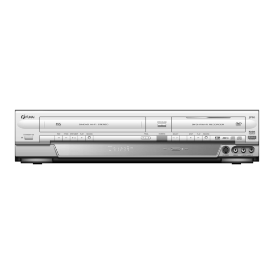
DRV-D2831
When servicing the deck
mechanism, refer to MK14 Deck
Mechanism Section.
Deck Mechanism Part No.:
N25E0FL
PAL
Advertisement
Table of Contents

Related Manuals for FUNAI DRV-D2831


Summary of Contents for FUNAI DRV-D2831
- Page 1 When servicing the deck I Specifications mechanism, refer to MK14 Deck I Preparation for Servicing Mechanism Section. I Adjustment Procedures I Schematic Diagrams Deck Mechanism Part No.: I CBA’s I Exploded views N25E0FL I Parts List DVD RECORDER & VIDEO CASSETTE RECORDER DRV-D2831...
-
Page 2: Table Of Contents
MAIN SECTION DVD RECORDER & VIDEO CASSETTE RECORDER DRV-D2831 Main Section I Specifications I Preparation for Servicing I Adjustment Procedures I Schematic Diagrams I CBA’s I Exploded Views I Parts List TABLE OF CONTENTS Specifications ............... . . 1-1-1 Laser Beam Safety Precautions . -
Page 3: Specifications
SPECIFICATIONS < VCR Section > Description Unit Minimum Nominal Maximum Remark 1. Video 1-1. Video Output (PB) Vp-p SP Mode 1-2. Video Output (R/P) Vp-p SP Mode, 1-3. Video S/N Y (R/P) W/O Burst 1-4. Video Color S/N AM (R/P) SP Mode 1-5. - Page 4 < DVD Section > Item Conditions Unit Nominal Limit 1. VIDEO 75 Ω load 1-1. Video Output Vp-p 1-2. S-Video Output 75 Ω load Y (Luminance) Vp-p 75 Ω load C (Chrominance) Vp-p 2. AUDIO 2-1. Output Level Vrms 2-2. Frequency Response DVD-VIDEO LPCM fs = 96 kHz 20 - 44 k...
-
Page 5: Laser Beam Safety Precautions
LASER BEAM SAFETY PRECAUTIONS This DVD player uses a pickup that emits a laser beam. Do not look directly at the laser beam coming from the pickup or allow it to strike against your skin. The laser beam is emitted from the location shown in the figure. When checking the laser diode, be sure to keep your eyes at least 30 cm away from the pickup lens when the diode is turned on. -
Page 6: Important Safety Precautions
IMPORTANT SAFETY PRECAUTIONS Product Safety Notice K. Crimp type wire connector The power transformer uses crimp type connectors Some electrical and mechanical parts have special which connect the power cord and the primary side safety-related characteristics which are often not evi- of the transformer. - Page 7 Safety Check after Servicing Examine the area surrounding the repaired location for damage or deterioration. Observe that screws, Chassis or Secondary Conductor parts, and wires have been returned to their original positions. Afterwards, do the following tests and con- Primary Circuit Terminals firm the specified values to verify compliance with safety standards.
-
Page 8: Standard Notes For Servicing
STANDARD NOTES FOR SERVICING Circuit Board Indications Pb (Lead) Free Solder When soldering, be sure to use the Pb free solder. 1. The output pin of the 3 pin Regulator ICs is indi- cated as shown. How to Remove / Install Flat Pack-IC Top View Bottom View 1. - Page 9 3. The flat pack-IC on the CBA is affixed with glue, so With Soldering Iron: be careful not to break or damage the foil of each (1) Using desoldering braid, remove the solder from all pin or the solder lands under the IC when removing pins of the flat pack-IC.
- Page 10 2. Installation (4) Bottom of the flat pack-IC is fixed with glue to the CBA; when removing entire flat pack-IC, first apply (1) Using desoldering braid, remove the solder from soldering iron to center of the flat pack-IC and heat the foil of each pin of the flat pack-IC on the CBA up.
- Page 11 Instructions for Handling Semi-conductors Electrostatic breakdown of the semi-conductors may occur due to a potential difference caused by electro- static charge during unpacking or repair work. 1. Ground for Human Body Be sure to wear a grounding band (1MΩ) that is prop- erly grounded to remove any static electricity that may be charged on the body.
-
Page 12: Preparation For Servicing
PREPARATION FOR SERVICING How to Enter the Service Mode About Optical Sensors Caution: An optical sensor system is used for the Tape Start and End Sensors on this equipment. Carefully read and follow the instructions below. Otherwise the unit may operate erratically. What to do for preparation Insert a tape into the Deck Mechanism Assembly and press the PLAY button. -
Page 13: Cabinet Disassembly Instructions
CABINET DISASSEMBLY INSTRUCTIONS 1. Disassembly Flowchart REMOVAL This flowchart indicates the disassembly steps to gain REMOVE/*UNHOOK/ LOC. PART Fig. access to item(s) to be serviced. When reassembling, UNLOCK/RELEASE/ Note follow the steps in reverse order. Bend, route, and UNPLUG/DESOLDER dress the cables as they were originally. Power Supply D6 4(S-9) - Page 14 Reference Notes CAUTION 1: Locking Tabs (L-1) and (L-2) are fragile. [5] Jack Bracket Be careful not to break them. (S-4) 1-1. Release five Locking Tabs (L-1). 1-2. Release three Locking Tabs (L-2) 1-3. Disconnect Connector (CN1505), and remove the Front Assembly. 2.
- Page 15 (S-13) (S-13) (S-14) (S-7) (S-8A) (S-14) (S-6A) (S-14) (S-6B) [8] Rear (S-13) Panel Unit (S-7) (S-15) (S-8B) (S-14) (S-7) (S-14) (S-16) (S-12) [14] VCR Chassis Unit CN1503 CN1504 [13] Bracket R Fig. D5 Fig. D7 [12] Rear Panel (S-11) (S-10) (S-11) [10] DC Fan Motor [9] Power...
- Page 16 [15] Deck Cylinder Assembly Assembly FE Head ACE Head Assembly SW507 LD-SW Ground Plate [19] AFV CBA [16] Power SW CBA [18] Rear [19] Main CBA Jack CBA [15] Deck Assembly [19] Main Cam Gear Desolder (S-17) from bottom Hole Shaft (S-18) Lead...
- Page 17 (S-19) (S-19) [20] Deck Pedestal [21] Front Bracket R (S-20) Fig. D9 3. How to Eject Manually < Method 1 > Note: When servicing, do not touch white resin part as shown below. When rotating the gear, be careful not to damage the gear. 1.
- Page 18 < Method 2 > Note: When servicing, do not touch white resin part 4. Release the other side of two Locking Tabs, and as shown below. remove the Clamper Assembly. 1. Remove the Top Cover, the Front Assembly and the DVD Mechanism & DVD Main CBA Assembly. Clamper Assembly Then, remove the DVD Mechanism Unit.
-
Page 19: Electrical Adjustment Instructions
ELECTRICAL ADJUSTMENT INSTRUCTIONS General Note: "CBA" is an abbreviation for "Circuit Board Assembly." NOTE: Figure 1 1.Electrical adjustments are required after replacing circuit components and certain mechanical parts. It is important to do these adjustments only after all repairs and replacements have been com- EXT. -
Page 20: How To Initialize The Dvd Recorder & Vcr
HOW TO INITIALIZE THE DVD RECORDER & VCR To put the program back at the factory-default, initialize the DVD recorder & VCR as the following procedure. < DVD Section > 1. Turn the DVD recorder on. 2. Confirm that no disc is loaded or that the disc tray is open. -
Page 21: Firmware Renewal Mode
FIRMWARE RENEWAL MODE 1. Turn the power on and remove the disc on the tray. 4. Select the firmware version pressing arrow buttons, then press [ENTER]. 2. To put the DVD recorder into version up mode, Fig. d appears on the screen and Fig. e appears press [CM SKIP], [6], [5], and [4] buttons on the on the VFD. - Page 22 5. After updating is finished, the tray opens automatically. Fig. f appears on the screen and Fig. g appears on the VFD. * Firmware Version differs depending on the models, and this indication is one example. Firm Update Mode ver. W2E3075H2D W2E3075H2D B/E Firmware Update End...
-
Page 23: Function Indicator Symbols
FUNCTION INDICATOR SYMBOLS < VCR Section > Note: If a mechanical malfunction occurs, the power is turned off. When the power comes on again after that by pressing [STANDBY-ON] button, an error message is displayed on the TV screen for 5 seconds. MODE INDICATOR ACTIVE When reel or capstan mechanism is not... - Page 24 < DVD Section > Note: If an error occurs, a message with the error number appears on the screen. Recording Error Error message You cannot record on this disc as Power Calibration Area is full. Error No. Error Message Solution Error Description Priority An error occurs during data reading.
- Page 25 Error Message Solution Error Description Priority Release the disc protect This disc is protected and not setting in the Disc Setting Disc Protected Disc. recordable. menu. Disc is full. Insert the recordable disc with There is no it in a space field. (No area for new recording) enough recording space.
-
Page 26: Block Diagrams
BLOCK DIAGRAMS Servo/System Control Block Diagram 1-11-1 E9709BLS... - Page 27 Digital Signal Process Block Diagram 1-11-2 E9709BLD...
- Page 28 Video Block Diagram 1-11-3 E9709BLV...
- Page 29 Video Input Select Block Diagram 1-11-4 E9709BLVIS...
- Page 30 Video Output Select Block Diagram 1-11-5 E9709BLVOS...
- Page 31 Audio Block Diagram 1-11-6 E9709BLA...
- Page 32 Audio Input/Output Select Block Diagram 1-11-7 E9709BLAS...
- Page 33 Hi-Fi Audio Block Diagram 1-11-8 E9709BLH...
- Page 34 Power Supply Block Diagram 1-11-9 E9709BLP...
-
Page 35: Schematic Diagrams / Cba's And Test Points
SCHEMATIC DIAGRAMS / CBA’S AND TEST POINTS Standard Notes WARNING Many electrical and mechanical parts in this chassis have special characteristics. These characteristics often pass unnoticed and the protection afforded by them cannot necessarily be obtained by using replacement components rated for higher voltage, wattage, etc. - Page 36 LIST OF CAUTION, NOTES, AND SYMBOLS USED IN THE SCHEMATIC DIAGRAMS ON THE FOLLOWING PAGES: 1. CAUTION: FOR CONTINUED PROTECTION AGAINST FIRE HAZARD, REPLACE ONLY WITH THE SAME TYPE FUSE. 2. CAUTION: Fixed Voltage (or Auto voltage selectable) power supply circuit is used in this unit. If Main Fuse (F1001) is blown, first check to see that all components in the power supply circuit are not defective before you connect the AC plug to the AC power supply.
- Page 37 Main 1/9 Schematic Diagram < VCR Section > 1-12-3 E9709SCM1...
- Page 38 Main 2/9, Power SW, Function & Sensor Schematic Diagram < VCR Section > FL601 MATRIX CHART P.SCAN REPEAT VCD VCR VCD VCR XP SP LP EP REPEAT P.SCAN 1-12-4 E9709SCM2...
- Page 39 Main 3/9 Schematic Diagram < VCR Section > 1-12-5 E9709SCM3...
- Page 40 Main 4/9 Schematic Diagram < VCR Section > 1-12-6 E9709SCM4...
- Page 41 Main 5/9 Schematic Diagram < VCR Section > 1-12-7 E9709SCM5...
- Page 42 Main 6/9 & Front Jack Schematic Diagram < VCR Section > 1-12-8 E9709SCM6...
- Page 43 Main 7/9 Schematic Diagram < VCR Section > 1-12-9 E9709SCM7...
- Page 44 Main 8/9 Schematic Diagram < VCR Section > E9709SCM8 1-12-10...
- Page 45 Main 9/9 Schematic Diagram < VCR Section > E9709SCM9 1-12-11...
- Page 46 Power Supply & Junction Schematic Diagram < VCR Section > CAUTION ! NOTE: CAUTION ! For continued protection against fire hazard, The voltage for parts in hot circuit is measured using Fixed voltage (or Auto voltage selectable) power supply circuit is used in this unit. replace only with the same type fuse.
- Page 47 Rear Jack Schematic Diagram < VCR Section > E9709SCRJ 1-12-13...
- Page 48 AFV Schematic Diagram < VCR Section > E9709SCAFV 1-12-14...
- Page 49 DVD Main 1/6 Schematic Diagram < DVD Section > 1-12-15 E9709SCD1...
- Page 50 DVD Main 2/6 Schematic Diagram < DVD Section > 1-12-16 E9709SCD2...
- Page 51 DVD Main 3/6 Schematic Diagram < DVD Section > 1-12-17 E9709SCD3...
- Page 52 DVD Main 4/6 Schematic Diagram < DVD Section > NOTE: 1. The order of pins shown in this diagram is different from that of actual IC601. 2. IC601 is divided into six and shown as IC601 (1/6) ~ IC601 (6/6) in this DVD Main Schematic Diagram Section. 1-12-18 E9709SCD4...
- Page 53 DVD Main 5/6 Schematic Diagram < DVD Section > NOTE: 1. The order of pins shown in this diagram is different from that of actual IC601. 2. IC601 is divided into six and shown as IC601 (1/6) ~ IC601 (6/6) in this DVD Main Schematic Diagram Section. 1-12-19 E9709SCD5...
- Page 54 DVD Main 6/6 Schematic Diagram < DVD Section > NOTE: 1. The order of pins shown in this diagram is different from that of actual IC601. 2. IC601 is divided into six and shown as IC601 (1/6) ~ IC601 (6/6) in this DVD Main Schematic Diagram Section. 1-12-20 E9709SCD6...
- Page 55 Main CBA Top View Sensor CBA Top View TO SENSOR CBA (END-SENSOR) BHF300F01011A J236 TO SENSOR CBA JK1-V-OUT (START-SENSOR) BHF300F01011B TP301 C-PB VR501 SW-P TP503 TP504 RF-SW TP501 S-INH 1-12-21 BE9700F01015A...
- Page 56 Main CBA Bottom View PIN 6 OF IC1515 WF10 PIN 1 OF CN1501 PIN 3 OF IC1502 PIN 5 OF CN1502 PIN 7 OF CN1502 PIN 9 OF CN1502 PIN 17 OF CN1502 1-12-22 BE9700F01015A...
- Page 57 Power SW CBA Top View Power SW CBA Bottom View Function CBA Top View Function CBA Bottom View BE9700F01015B BE9700F01015C Front Jack CBA Top View Front Jack CBA Bottom View BE9700F01015D 1-12-23...
- Page 58 Power Supply CBA Top View CAUTION ! CAUTION ! Because a hot chassis ground is present in the power For continued protection against fire hazard, Fixed voltage (or Auto voltage selectable) power supply circuit is used in this unit. supply circut, an isolation transformer must be used. replace only with the same type fuse.
- Page 59 Power Supply CBA Bottom View CAUTION ! CAUTION ! Because a hot chassis ground is present in the power For continued protection against fire hazard, Fixed voltage (or Auto voltage selectable) power supply circuit is used in this unit. supply circut, an isolation transformer must be used. replace only with the same type fuse.
- Page 60 Junction CBA Top View Junction CBA Bottom View AFV CBA Top View AFV CBA Bottom View BE9700F01022B BE6800F01091 Rear Jack CBA Bottom View Rear Jack CBA Top View BH9700F01022C 1-12-26...
-
Page 61: Waveforms
WAVEFORMS NOTE: Input: COLOR BAR SIGNAL (WITH 1KHz AUDIO SIGNAL) TP301 UPPER Pin 5 of CN1502 Pin 6 of IC1515 TP504 LOWER C-PB 0.2V RF-SW VIDEO-Cb 0.2V 20µs VIDEO-CVBS 0.5V 20µs J236 UPPER Pin 7 of CN1502 Pin 1 of CN1501 TP504 WF10 LOWER... -
Page 62: Wiring Diagram < Vcr Section
WIRING DIAGRAM < VCR SECTION > 1-14-1 E9709WI... -
Page 63: Wiring Diagram < Dvd Section
WIRING DIAGRAM < DVD SECTION > 1-14-2 E9709WID... -
Page 64: Ic Pin Function Descriptions
IC PIN FUNCTION DESCRIPTIONS < VCR Section > Signal Function Name IC501( SERVO / SYSTEM CONTROL IC ) AUDIO- 28 OUT Audio Mute Control Signal MUTE-2 Signal DVD- Function Name DVD Audio Mute Control 29 OUT AUDIO- Signal MUTE Input Signal from Pin 8 of SC2-IN SCART2 Not Used... - Page 65 Signal Signal Function Function Name Name Control SCART 1 8Pin Drum Motor Phase/ D-PFG 60 OUT 8POUT-2 Level by using 8POUT-1 Frequency Generator and 8POUT-2 AMPVREF V-Ref for CTL AMP Not Used Not Used AMPVREF V-Ref for CTL AMP SYSTEM- 63 OUT System Reset Signal RESET...
- Page 66 IC612 ( FIP DRIVER ) Signal Name Function Name Signal Name Function Name POWER- Power LED Signal Output LED (NU) VCR Mode LED Signal OUT VCR-LED Output Grid Output DVD Mode LED Signal OUT DVD-LED Output Not Used Oscillator Input Power Supply Not Used DRV-DIN...
-
Page 67: Lead Identifications
LEAD IDENTIFICATIONS 2SA1175(F,H,J) 2SA1015-GR(TPE2) 2SC3266-Y(TPE2) 2SC2785(F,H,J) MID-32A22F 2SA1015-GR(TE2 F T) 2SA1020(Y) BA1F4M-T PT204-6B-12 2SC1815-BL(TPE2) 2SA1020-Y(TE6 F M) BN1F4M-T 2SC1815-GR(TPE2) KTA1281(Y) KRA103M-AT/P 2SC1815-BL(TE2 F T) KTA1281Y-AT/P KRC103M 2SC1815-GR(TE2 F T) KTC3203(Y) KRC103M-AT/P 2SC1815-Y(TE2 F T) KTC3203-Y-AT/P KTA1266(GR) 2SC1815-Y(TPE2) KTC3205-Y-AT/P KTA-1266-GR-AT/P 2SC2120-Y(TPE2) KTC3205(Y) KTA1267(GR,Y) 2SC2120-Y(TE2 F T) -
Page 68: Exploded Views
EXPLODED VIEWS Cabinet 2B62 2L065 2L011 2L011 2L071 See Electrical Parts List 2L071 2L071 for parts with this mark. 2L071 2L081 2L011 2L082 2L062 2L083 2L044 2L100 2B60 FM1001 2L081 2L044 AFV CBA 2L033 JW2002 2L044 2L011 Sensor CBA 2L033 Rear Jack CBA 2B14 Power Supply CBA... - Page 69 Packing X20A X20B X22A X22B X20C X20D X22C X22D X20E X20F X22E X22F X20G X22G 1-17-2 E9709PEX...
-
Page 70: Mechanical Parts List
MECHANICAL PARTS LIST PRODUCT SAFETY NOTE: Products marked with a Ref. No. Description Part No. ! have special characteristics important to safety. 2L060 P-TIGHT SCREW 3X8 BIND + or GBMP3080 Before replacing any of these components, read SCREW P-TIGHT M3X8 BIND HEAD+ GBJP3080 carefully the product safety notice in this service 2L061... -
Page 71: Electrical Parts List
ELECTRICAL PARTS LIST PRODUCT SAFETY NOTE: Products marked with a Ref. No. Description Part No. ! have special characteristics important to safety. C313 ELECTROLYTIC CAP . 1µF/50V M H7 CE1JMASSL1R0 Before replacing any of these components, read C314 CHIP CERAMIC CAP .(1608) B K 0.01µF/50V CHD1JK30B103 carefully the product safety notice in this service C315... - Page 72 Ref. No. Description Part No. Ref. No. Description Part No. C413 CHIP CERAMIC CAP .(1608) F Z 0.1µF/50V or CHD1JZ30F104 CHIP CERAMIC CAP . FZ Z 0.1µF/50V CHD1JZ3FZ104 CHIP CERAMIC CAP .(1608) F Z 0.1µF/25V or CHD1EZ30F104 C502 CHIP CERAMIC CAP .(1608) B K 0.022µF/50V or CHD1JK30B223 CHIP CERAMIC CAP .
- Page 73 Ref. No. Description Part No. Ref. No. Description Part No. C612 CHIP CERAMIC CAP .(1608) B K 4700pF/50V CHD1JK30B472 CHIP CERAMIC CAP . FZ Z 0.1µF/50V CHD1JZ3FZ104 C614 CHIP CERAMIC CAP .(1608) F Z 0.1µF/50V or CHD1JZ30F104 C1540 CHIP CERAMIC CAP .(1608) F Z 0.1µF/50V or CHD1JZ30F104 CHIP CERAMIC CAP .(1608) F Z 0.1µF/25V or CHD1EZ30F104...
- Page 74 Ref. No. Description Part No. Ref. No. Description Part No. C1586 CHIP CERAMIC CAP .(1608) CH J 47pF/50V or CHD1JJ3CH470 C1649 CHIP CERAMIC CAP . B K 2200pF/50V CHD1JK30B222 CHIP CERAMIC CAP . CG J 47pF/50V CHD1JJ3CG470 C1657 ELECTROLYTIC CAP . 1µF/50V M or CE1JMASDL1R0 C1588 CHIP CERAMIC CAP .(1608) CH J 47pF/50V or...
- Page 75 Ref. No. Description Part No. Ref. No. Description Part No. SWITCHING DIODE 1SS133(T-77) QDTZ001SS133 D502 LED(GREEN) 204-10GD/S957 NPQZ10GDS957 IC301 IC Y/C/A LA71750EM-MPB-E QSZBA0RSY020 D503 LED(GREEN) 204-10GD/S957 NPQZ10GDS957 IC451 IC HIFI LA72648M-MPB-E QSZBA0RSY033 D510 SWITCHING DIODE 1N4148M or NDTZ01N4148M IC501 SYSCON IC M3776AMCH-AD4GP QSZAC0RHT068 SWITCHING DIODE 1SS133(T-77) QDTZ001SS133...
- Page 76 Ref. No. Description Part No. Ref. No. Description Part No. TRANSISTOR 2SC1815-Y(TPE2) or QQSY02SC1815 TRANSISTOR 2SC2785(F) or QQSF02SC2785 TRANSISTOR 2SC1815-GR(TPE2) QQS102SC1815 TRANSISTOR KTC3199(Y) or NQSY0KTC3199 Q401 CHIP TRANSISTOR RN1511(TE85R.F) or QQ2Z0RN1511F TRANSISTOR KTC3199 or NQS40KTC3199 CHIP TRANSISTOR FMG4A T148 or QQ2Z000FMG4A TRANSISTOR 2SC1815-Y(TPE2) or QQSY02SC1815...
- Page 77 Ref. No. Description Part No. Ref. No. Description Part No. TRANSISTOR 2SC1815-Y(TPE2) or QQSY02SC1815 TRANSISTOR KTC3199-GR-AT/P or NQS4KTC3199P TRANSISTOR 2SC1815-GR(TPE2) QQS102SC1815 TRANSISTOR 2SC1815-Y(TE2 F T) or QQSY2SC1815F Q1525 TRANSISTOR KTC3199-Y -AT/P or NQSYKTC3199P TRANSISTOR 2SC1815-GR(TE2 F T) or QQS12SC1815F TRANSISTOR KTC3199-GR-AT/P or NQS4KTC3199P TRANSISTOR 2SC2785(J) or QQSJ02SC2785...
- Page 78 Ref. No. Description Part No. Ref. No. Description Part No. CARBON RES. 1/4W J 820 Ω CARBON RES. 1/4W J 10k Ω R401 RCX4JATZ0821 RCX4JATZ0103 CARBON RES. 1/6W J 100 Ω or CARBON RES. 1/6W J 10k Ω or R402 RCX6JATZ0101 R545 RCX6JATZ0103...
- Page 79 Ref. No. Description Part No. Ref. No. Description Part No. CARBON RES. 1/4W J 4.7k Ω CHIP RES. 1/10W J 6.8k Ω RCX4JATZ0472 R1567 RRXAJR5Z0682 CARBON RES. 1/6W J 2.7k Ω or CARBON RES. 1/6W J 3.3k Ω or R653 RCX6JATZ0272 R1568 RCX6JATZ0332...
- Page 80 Ref. No. Description Part No. Ref. No. Description Part No. CARBON RES. 1/4W J 75 Ω R1659 RCX4JATZ0750 SW507 ROTARY MODE SWITCH SSS-53MD SSR0106KB003 CARBON RES. 1/4W J 75 Ω R1660 RCX4JATZ0750 SW521 TACT SWITCH KSM0614B or SST0101HH013 CARBON RES. 1/4W J 75 Ω R1661 RCX4JATZ0750 TACT SWITCH SKQSAF001A or...
- Page 81 POWER SW CBA SENSOR CBA Ref. No. Description Part No. Ref. No. Description Part No. POWER SW CBA (MCV-B) ---------- SENSOR CBA 1VSA11699 Consists of the following: Consists of the following: DIODE TRANSISTORS D671 LED(RED) 204HD/E NPQZ00204HDE Q503 PHOTO TRANSISTOR PT204-6B-12 or NPWZT2046B12 SWITCHES PHOTO TRANSISTOR MID-32A22F...
- Page 82 Ref. No. Description Part No. Ref. No. Description Part No. C2014 CERAMIC CAP . B K 0.01µF/500V CCD2JKP0B103 L1002 BEAD CORE ASSEMBLY E9700ED 1VSA11692 DIODES L1003! LINE FILTER 56MH TLF14CB5630R2 or LLBG00ZTU022 LINE FILTER 50MH LF-4D-E503 LLBG00ZKQ009 D013 RECTIFIER DIODE BA158 or NDQZ000BA158 L1004 BEAD CORE B16 RH 3.5X10X1.3...
- Page 83 Ref. No. Description Part No. Ref. No. Description Part No. CARBON RES. 1/4W J 1k Ω RCX4JATZ0102 ZENER DIODE MTZJT-7711A QDTA00MTZJ11 CARBON RES. 1/6W J 100k Ω or R1036 RCX6JATZ0104 D2004 ZENER DIODE DZ-11BSAT265 or NDTA00DZ11BS CARBON RES. 1/4W J 100k Ω RCX4JATZ0104 ZENER DIODE MTZJT-7711A QDTA00MTZJ11...
- Page 84 AFV CBA Ref. No. Description Part No. AFV CBA 1VSA11738 Consists of the following: CAPACITORS CHIP CERAMIC CAP .(1608) F Z 0.1µF/50V or CHD1JZ30F104 CHIP CERAMIC CAP .(1608) F Z 0.1µF/25V or CHD1EZ30F104 CHIP CERAMIC CAP . FZ Z 0.1µF/50V CHD1JZ3FZ104 CHIP CERAMIC CAP .
- Page 85 DRV-D2831 E9709ED 2005-10-27...
Need help?
Do you have a question about the DRV-D2831 and is the answer not in the manual?
Questions and answers