Icom ID-1 Service Manual
Digital
Hide thumbs
Also See for ID-1:
- Addendum (1 page) ,
- Instruction manual (124 pages) ,
- Instruction manual (124 pages)
Table of Contents
Advertisement
Quick Links
Download this manual
See also:
Instruction Manual
Advertisement
Table of Contents

Subscribe to Our Youtube Channel
Related Manuals for Icom ID-1


Summary of Contents for Icom ID-1
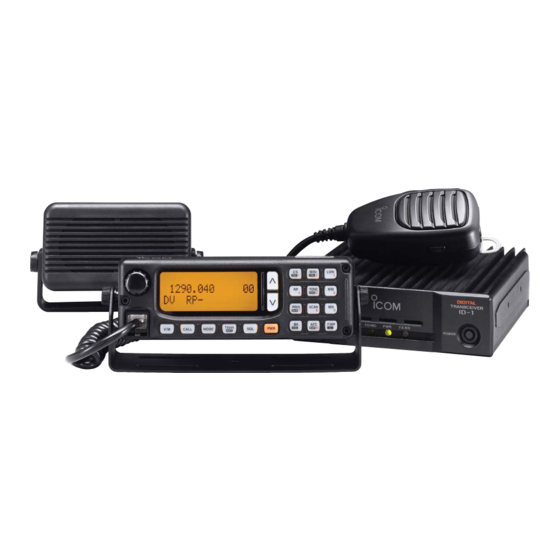
- Page 1 SERVICE MANUAL DIGITAL TRANSCEIVER S-14120IZ-C1 May. 2005...
- Page 2 8. READ the instructions of test equipment thoroughly before connecting equipment to the transceiver. Icom, Icom Inc. and logo are registered trademarks of Icom Incorporated (Japan) in the United States, the United Kingdom, Germany, France, Spain, Russia and/or other countries.
-
Page 3: Table Of Contents
ID-1 ........ - Page 4 SECTION 1 SPECIFICATIONS ■ GENERAL • Frequency coverage : 1240.000–1300.000 MHz • Type of emission : FM, GMSK (Digital) • Transmission speed (theoretical value) : Data 128 kbps Digital voice 4.8 kbps • Codec : AMBE (2.4 kbps) • Number of memory channel : 105 (incl.
- Page 5 SECTION 2 INSIDE VIEWS • MAIN UNIT Top view APC amplifier* (IC1250: TA75501F) RF amplifier (Q1: NE34018) 1st VCO circuit Power amplifier* (IC1160: RA18H1213G1) AF power amplifier (IC1551: LA4425) PLL reference Demodulator IC oscillator [DV mode], [FM mode] (X400: CR662) (IC191: TA33136) 2nd VCO circuit MSK receiver IC...
- Page 6 SECTION 3 DISASSEMBLY INSTRUCTIONS 2 Unsolder 11 points C. 3-1 ID-1 3 Unscrew 2 screws D, and remove the ANT connector E. • REMOVING THE LOGIC-1 UNIT 4 Take off the cable F from the chassis. 1 Unscrew 1 screw A, and remove the cover B.
-
Page 7: Section Circuit Descripiton
SECTION 4 CIRCUIT DESCRIPTION 4-1 RECEIVER CIRCUITS The RF signals from the bandpass filter (FI2) are mixed with the 1st LO signal, where come from the 1st VCO cir- 4-1-1 ANTENNA SWITCHING CIRCUIT (MAIN UNIT) cuit, at the 1st mixer circuit (IC71) to produce a 243.95 The antenna switching circuit functions as a low-pass filter MHz 1st IF signal. - Page 8 4-1-5 DEMODULATOR CIRCUITS (MAIN UNIT) The demodulated data signals from the MSK receiver IC (IC271, pin 13) are amplified at IC343 (pins 1, 2) and then • DV MODE applied to the mode switch (IC342, pins 1, 6). The demodulator IC (IC191) contains the 3rd mixer, limiter amplifier, quadrature detector, active filter and noise ampli- The switched signals from the mode switch (IC342, pin 1) fier, etc.
- Page 9 signals are applied to the CPU (IC50) via the FPGA IC 4-1-8 SQUELCH CIRCUITS (MAIN UNIT) (IC200). • DIGITAL CODE/CALL SIGN SQUELCH (DV MODE ONLY) The digital code/call sign squelch circuit detects matched • DV MODE (VOICE OPERATION) digital code/call sign and opens the squelch only when The digital audio signals from the CPU (IC50) are applied receiving a signal containing a matching digital code/call to the AMBE CODEC IC (IC2) for code expansion, and are...
-
Page 10: Transmitter Circuits
"DAMOD" signal. The converted digital audio signals are applied to the AMBE CODEC IC (IC2) for code com- While connecting the microphone to ID-1, the AF signals pression and are then applied to the CPU (IC50). from the microphone (J1600, pin 6) are applied to the micro-... -
Page 11: Pll Circuits
and then mixed with the amplified I/Q baseband signals. The The power amplifi ed signal from the power amplifi er (IC1160, modulated signal is output from pin 14. pin 4) is passed through the antenna switch (D1160), SWR detector circuit (D1166, D1170), low-pass fi lter which The modulated signal (IC890, pin 14) is passed through the contains strip-line and C1198, and then applied to the bandpass (FI880) and low-pass (L892, L893, C904–C908) -
Page 12: Power Supply Circuits
signal from the 1st VCO (Q471, Q472, D471) is applied to 4-4 POWER SUPPLY CIRCUITS the buffer amplifi ers (Q473, Q474) and is then applied to the 4-4-1 LOGIC-1 UNIT VOLTAGE LINE PLL IC (IC400, pin 6). Line Description The PLL IC contains a prescaler, programmable counter, Common 5 V controlled by the +5 V regula- programmable divider and phase detector, etc. -
Page 13: Port Allocation
4-5 PORT ALLOCATIONS 4-5-1 CPU (LOGIC-1 UNIT; IC50) Port Port Description Description number name number name Outputs control signal to the TX power Input port for up/down signal from the PCON MU/D controller (MAIN unit; Q1250). connected microphone. Input port for the PLL unlock signal. Input port for the noise signal from the ULCK NOIS... -
Page 14: Preparation
SECTION 5 ADJUSMENT PROCEDURESE 5-1 PREPARATION When adjusting ID-1, ADJUSTMENT SOFTWARE, JIG CABLE (see illustration on page 5-2) and OPC-1127 are re- USB CABLE quired. ▄ REQUIRED TEST EQUIPMENT EQUIPMENT GRADE AND RANGE EQUIPMENT GRADE AND RANGE Output voltage : 13.8 V DC Frequency range : 300–3000 Hz... - Page 15 • CONNECTION DC power supply Modulation Attenuator 13.8 V, 10 A or more analyzer 50 dB or 60 dB RF power meter 50 Ω, 20 W Standard signal generator 0.1–1500 MHz –127 to –17 dBm (0.1 µV to 32 mV) Coution DO NOT transmit while an SSG is...
-
Page 16: Pll And Codec Adjustment
5-2 PLL AND CODEC ADJUSTMENT MEASUREMENT ADJUSTMENT ADJUSTMENT ADJUSTMENT CONDITION VALUE UNIT LOCATION UNIT ADJUST FPGA 1 • Operating freq. : 1240.00 MHz LOGIC-1 Connect a frequency 16.3840 MHz LOGIC-1 C202 FREQUENCY • Mode : DD mode unit counter to the check unit [ Set FPGA •... - Page 17 • MAIN AND LOGIC-1 UNITS PLL lock voltage check point C202 FPGA frequency adjustment C215 CP200 PLL lock voltage FPGA frequency check point check point CP.I CP.IR I/Q balance check point CP.Q CP.QR 5 - 4...
-
Page 18: Transmitter Adjustment
CURRENT mum counterclockwise. panel between the DC power from the pre- unit [ FPGA D.C. • Preset "IQ Direct-current output" supply and ID-1. set position. voltage ad- justment • Operating freq. : 1300.00 MHz 100 mA higher MAIN R1086 /DV I ] •... - Page 19 • MAIN AND LOGIC-1 UNITS R1251 TX power adjustment R1087 R1086 YGR current adjustment YGR carrent adjustmentent CP30 FM carrier check point CP207 CP207 DSP input level check point R1704 FM deviation adjustment R1707 DSP input level adjustment 5 - 6...
-
Page 20: Receiver Adjustment
5-4 RECEIVER ADJUSTMENT ADJUSTMENT ITEM ADJUSTMENT CONDITION OPERATION SQUELCH • Operating freq. : 1270.00 MHz • Push [ENTER] on the connected computer key- LEVEL • Mode : FM mode board to set to "SQL adjustment/FM thresh" level. [ SQL adjustment •... -
Page 21: Section 6 Parts List
SECTION 6 PARTS LIST [MAIN UNIT] [MAIN UNIT] ORDER ORDER DESCRIPTION DESCRIPTION LOCATION LOCATION Q1351 1590000430 S.TR DTC144EUA T106 35.6/32.9 IC71 1110004470 S.IC µPC2721GV-E1 45.5/76.4 Q1352 1590000430 S.TR DTC144EUA T106 48.2/89.4 IC191 1110003490 S.IC TA31136FN (D,EL) 46.5/29.9 Q1460 1530002280 S.TR 2SC4081 T106 S 5.9/75.3 IC271... - Page 22 [MAIN UNIT] [MAIN UNIT] ORDER ORDER DESCRIPTION DESCRIPTION LOCATION LOCATION 6200006990 S.COL ELJRE 56NG-F 40.4/78.9 L1606 6200006990 S.COL ELJRE 56NG-F 114.8/10.8 6200006990 S.COL ELJRE 56NG-F 47.5/72.2 L1607 6200006990 S.COL ELJRE 56NG-F 115.8/11.7 6200006990 S.COL ELJRE 56NG-F 42.3/68.8 L1608 6200006990 S.COL ELJRE 56NG-F 95.2/.9 6200009350 S.COL ELJRE R22G-F3 41.5/61.3...
- Page 23 [MAIN UNIT] [MAIN UNIT] ORDER ORDER DESCRIPTION DESCRIPTION LOCATION LOCATION R291 7030003680 S.RES ERJ3GEYJ 104 V (100 kΩ) 71.3/22.7 R778 7030003440 S.RES ERJ3GEYJ 102 V (1 kΩ) 26.7/41.8 R292 7510001670 S.TMR NTCG16 4BH 103KT 72.1/40.3 R779 7030003650 S.RES ERJ3GEYJ 563 V (56 kΩ) 26.4/38 7030003320 S.RES ERJ3GEYJ 101 V (100 Ω) R293...
- Page 24 [MAIN UNIT] [MAIN UNIT] ORDER ORDER DESCRIPTION DESCRIPTION LOCATION LOCATION R1412 7030003640 S.RES ERJ3GEYJ 473 V (47 kΩ) 43.1/18 R1708 7030003480 S.RES ERJ3GEYJ 222 V (2.2 kΩ) 79/13.1 7030003320 S.RES ERJ3GEYJ 101 V (100 Ω) R1413 40.5/18 R1709 7030005331 S.RES ERA3YED 562V 79/14.4 R1414 7030003800 S.RES ERJ3GEYJ 105 V (1 MΩ)
- Page 25 [MAIN UNIT] [MAIN UNIT] ORDER ORDER DESCRIPTION DESCRIPTION LOCATION LOCATION C273 4030006900 S.CER C1608 JB 1H 103K-T 82/40.6 C503 4550006250 S.TAN TEESVA 1A 106M8L 18.8/70.3 C274 4030006900 S.CER C1608 JB 1H 103K-T 76.3/42.5 C504 4030009560 S.CER C1608 CH 1H R75B-T 28.6/79.3 C275 4030006900 S.CER C1608 JB 1H 103K-T...
- Page 26 [MAIN UNIT] [MAIN UNIT] ORDER ORDER DESCRIPTION DESCRIPTION LOCATION LOCATION C835 4030011600 S.CER C1608 JB 1E 104K-T 52.5/30.5 C1189 4030009510 S.CER C1608 CH 1H 010B-T 77.8/107.8 C836 4550006250 S.TAN TEESVA 1A 106M8L 54.5/31.3 C1191 4030007090 S.CER C1608 CH 1H 470J-T 86.8/121.8 C837 4030007130 S.CER C1608 CH 1H 101J-T...
- Page 27 [MAIN UNIT] [MAIN UNIT] ORDER ORDER DESCRIPTION DESCRIPTION LOCATION LOCATION C1477 4030006860 S.CER C1608 JB 1H 102K-T 35.2/15.5 C1675 4550006760 S.TAN TEESVB21A336M8R 92/20.5 C1478 4030008470 S.CER C1608 JB 1H 272K-T 42.4/9.9 C1676 4510005600 S.ELE ECEV1CS100SR 88.4/19.7 C1479 4030006850 S.CER C1608 JB 1H 471K-T 45/11.2 C1677 4030008850 S.CER C1608 JB 1H 123K-T...
- Page 28 [MAIN UNIT] [LOGIC-1 UNIT] ORDER ORDER DESCRIPTION DESCRIPTION LOCATION LOCATION EP403 6910012350 S.BEA MMZ1608Y 102BT 20.8/63 Q501 1590000430 S.TR DTC144EUA T106 76.6/66.1 EP404 6910012350 S.BEA MMZ1608Y 102BT 14.4/60.4 Q502 1530002280 S.TR 2SC4081 T106 S 67.9/72.3 EP405 6910012350 S.BEA MMZ1608Y 102BT 21.3/66.3 Q503 1520000200 S.TR...
- Page 29 [LOGIC-1 UNIT] [LOGIC-1 UNIT] ORDER ORDER DESCRIPTION DESCRIPTION LOCATION LOCATION 7030003360 S.RES ERJ3GEYJ 221 V (220 Ω) 50.9/43.3 R305 7030003480 S.RES ERJ3GEYJ 222 V (2.2 kΩ) 67.4/13 7030003340 S.RES ERJ3GEYJ 151 V (150 Ω) 48.6/50.2 R306 7030003480 S.RES ERJ3GEYJ 222 V (2.2 kΩ) 63.7/16.8 R100 7030003640 S.RES ERJ3GEYJ 473 V (47 kΩ)
- Page 30 [LOGIC-1 UNIT] [LOGIC-1 UNIT] ORDER ORDER DESCRIPTION DESCRIPTION LOCATION LOCATION R559 7030003530 S.RES ERJ3GEYJ 562 V (5.6 kΩ) 12.4/62.6 C162 4030007000 S.CER C1608 CH 1H 090D-T 93.3/8.5 R560 7030003680 S.RES ERJ3GEYJ 104 V (100 kΩ) 17.8/52.2 C200 4030011600 S.CER C1608 JB 1E 104K-T 34.6/54.2 R561 7030003560 S.RES ERJ3GEYJ 103 V (10 kΩ)
- Page 31 [LOGIC-1 UNIT] [LOGIC-1 UNIT] ORDER ORDER DESCRIPTION DESCRIPTION LOCATION LOCATION C443 4030011810 S.CER C1608 JB 1A 224K-T 71.3/18.6 IC1160 1150002190 IC RA18H1213G1-21 C500 4510004640 S.ELE ECEV1CA470SP 84.4/63.5 C501 4030011600 S.CER C1608 JB 1E 104K-T 84.1/66.4 C502 4030011600 S.CER C1608 JB 1E 104K-T 86.5/67 6510004910 CNR NR-DS-E 01...
- Page 32 [RC-24] (Optional for some version) [RC-24] (Optional for some versions) ORDER ORDER DESCRIPTION DESCRIPTION LOCATION LOCATION 7030003680 S.RES ERJ3GEYJ 104 V (100 kΩ) 124.2/25.8 5040002470 S.LED FY1112H 31/26.4 7030003680 S.RES ERJ3GEYJ 104 V (100 kΩ) 124.2/12.8 5040002470 S.LED FY1112H 42.5/26.4 7030003680 S.RES ERJ3GEYJ 104 V (100 kΩ) 124.2/14.1 5040002470 S.LED FY1112H...
-
Page 33: Semi-Conductor Information
SECTION 7 SEMI-CONDUCTOR INFORMATION • TRANSISTORS AND FET’s 2SA1362 GR 2SA1586 GR 2SB798 DK 2SB934 P 2SC4081 R (Symbol: AEG) (Symbol: SG) (Symbol: DK) (Symbol: None) (Symbol: BR) 2SC4081 S 2SC4215 O 2SC4226 R25 2SC4684 (B type) 2SC5107 O (Symbol: BS) (Symbol: QO) (Symbol: R25) (Symbol: 2-7B2A) - Page 34 • DIODES 1SS355 1SS364 1SS372 1SV239 1SV245 (Symbol: A) (Symbol: BF) (Symbol: N9) (Symbol: TC) (Symbol: T3) 1SV282 1SV307 1SV308 DA204 U DSA3A1 (Symbol: TD) (Symbol: TX) (Symbol: TX) (Symbol: K) (Symbol: Green) green HSM88AS HSU88TRF MA2S077 MA2S728 MA111 (Symbol: C1) (Symbol: 9) (Symbol: S) (Symbol: B)
- Page 35 SECTION 8 MECHANICAL PARTS AND DISASSEMBLY 8-1 ID-1 [CHASSIS PARTS] [ACCESSORIES] REF.NO. ODER NO. DESCRIPTION QTY. REF. ORDER. NO. DESCRIPTION QTY. EP1160 6910000970 DL-20P 2.6-3-1.2H Optional product Microphone HM-118N EP1162 6910000970 DL-20P 2.6-3-1.2H Optional product Speaker SP-22 IC1160 1150002190 RA18H1213G1-21...
-
Page 36: Front Unit
8-2 RC-24 [CHASSIS PARTS] REF.NO. ODER NO. DESCRIPTION QTY. 5030002180 TSC0712-UFTDHW 8930048320 SRCN-2140-SP-N-W 8210015740 2140 Front Panel 8930047980 2140 LCD Holder 8930048290 2140 LCD Filter 8210015770 2140 Reflector 8610009840 Knob N234 8810008760 Screw PH BT M2x8 NI-ZU MP10 8930038230 1765 Rear Seal MP12 8810009060 Screw M3x6 ZK MP13... - Page 37 MP39 ( M ) MP65 ( M ) MP65 ( M ) • ID-1 MP70 ( M ) MF1 ( C ) MP30 ( M ) MP65 ( M ) W1330 ( M ) MP2 ( C ) J1 ( C )
- Page 38 • RC-24 MP12 ( C ) W1 ( C ) S21 ( F ) MP9 ( C ) J1 ( F ) MP10 ( C ) MP9 ( C ) MP9 ( C ) MP9 ( C ) MP13 ( C ) MP4 ( C ) MP3 ( C ) EP2 ( C )
-
Page 39: Section 9 Board Layouts
SECTION 9 BOARD LAYOUTS 9-1 MAIN UNIT • TOP VIEW V135 CHASSIS J1 V130 MP69 J1750 R1252 D1330 W1262 CP160 V125 C1330 W1166 C1751 C1264 D1750 R1751 V120 C1201 J1550 J1800 R1086 to LOGIC-1 unit J401 CP30 V115 R1561 C1340 C1755 CP30 V110... - Page 40 • BOTTOM VIEW V135 V130 C1256 L1164 R1255 W1261 R1254 R1169 L1250 EP1751 V125 R1256 C1251 C1200 IC1250 L1613 C1207 EP1750 R1020 C1569 V120 D1252 C1268 IC1251 C1253 V115 C1374 R1259 C1267 W1029 C1375 V110 C1347 C1118 C1329 Q1330 L1805 C1342 C1341 C1372...
-
Page 41: Logic-1 Unit
J401 to MAIN unit J1800 9-2 LOGIC-1 UNIT • TOP VIEW B6046B C514 IC504 J401 IC500 C518 Q502 D502 L551 L550 IC503 R501 R512 C519 D501 R563 J401 R513 R511 C557 C407 L210 C502 L501 R500 Q501 D503 C504 IC51 C509 Q500 C550... - Page 42 J100 to ETHERNET/USB connector • BOTTOM VIEW J100 J100 L420 L421 C421 L510 C416 C521 C556 C503 C500 R556 R562 R550 R116 R551 C552 L101 R552 L100 R558 L552 R553 R115 IC201 R199 R561 R211 R568 Q550 IC100 IC553 T100 C579 IC52 C560...
- Page 43 9-3 RC-24 • TOP VIEW B-5779D [CS] [MHz] [LOW] DS11 [RP] [TONE] [MW] [DIAL] [PRIO] [SCAN] [MN] [MIC] DS13 DS10 [BK] [AFC] [F.INP] [V/M] [CALL] [MODE] [TXinh] [SQL] [PWR] DS14 DS15 DS16 H100 H105 H110 H115 H120 H125 H130 H135 H140 H145 to MIC...
- Page 44 • BOTTOM VIEW EP24 EP23 EP22 H145 H140 H135 H130 H125 H120 H115 H110 H105 H100 to ID-1 MP80 9 - 6...
-
Page 45: Block Diagram
SECTION 10 BLOCK DIAGRAM 10-1 MAIN UNIT ��� ��� ��� �� ��� �������������� ������������ ����������� ������������� �������������� ����������� ������������ �������������� ��� ��� ��� ��� ��� ��� ��� ��� ��� ��� ��� ��� ���� ��� �� ��4����������� ����� ����� ������ ������ �����... -
Page 46: Logic-1 Unit
10-2 LOGIC-1 UNIT 10-3 RC-24 ����� ����������� ����������� �������������� ����� ���� �� ���� ���� ��� ��� ��� ������� ������ ���� �������������� ��� ��� �� ��� ��� �������������� ������������� ������������� ���� �� ��� ����� ��� ������������ ������������� ����������� ������������� ������������ ����������� ���... -
Page 47: Voltage Diagram
SECTION 11 VOLTAGE DIAGRAM 11-1 MAIN UNIT ������������ ��������� ���� �� �� ��������������� ������ ����� ���� ��������� ����� ���� ����� ����� ������������� ����� ���������� ��������� ����� ���� ����� ������� ���������� ���� ������������� ����� ����� � ��������� ���� �� �������� ���� �����... - Page 48 ���� ���� ��� ������ �������������� �� �� ������������ �������� �������� ����� �������� �������� ����� ���� ����� ���� ���� �������� ���� ���� �������� ������ ����� ������ � ����� ������ ��� ���������������� ���� �������� �������� ����� ���������������� ��� ����� ��� ����� ������ ��������...
- Page 49 ������������ ���� ���� ��� ������ ����� ��� �������� ����� ����� �� ����� ����� ����� ��� ����� �������� ������ ����� ����� ����� ����� ����� � ��������� ��� ���� ����� �������� ���� ���� ������ ��� ��� ��� ��� ����� ����� �������� ����� �...
-
Page 50: Logic-1 Unit
11-2 LOGIC-1 UNIT ��������������� ����� �������� ����� ���� ���������� �������� � � � � � �������� ����������� ����� ��������� � � � �� ���� ��� � � �� ����������� ��� � �� ������� ��� � � � �� ������� ��� �... - Page 51 ��������������� ���� ����������� ��� �� � ���� �� � �� � �������� �� � �� � ����� �� � �� � ������������ ���� �������� �� � ���� �������� �� � ���� �������� �� �� ���� �������� �� �� �� �� ��...
- Page 52 11-3 RC-24 ����� �� �� �� �� �� �� �� �� ��� ��� ��� ��� ��� � � � ����� ����� �� �� �� �� �� �� �� ��� �� ��� �� �� ��� �� �� �� ��� �� ��� ��...
- Page 53 Phone : +34 (93) 590 26 70 Fax : +34 (93) 589 04 46 Glenwood Centre #150-6165 Highway 17 Delta, B.C., V4K 5B8, Canada : http://www.icomspain.com E-mail : icom@icomspain.com Phone : +1 (604) 952-4266 Fax : +1 (604) 952-0090 : http://www.icomcanada.com E-mail : info@icomcanada.com Unit 9, Sea St., Herne Bay, Kent, CT6 8LD, U.K.
- Page 54 S-14120IZ-C1 1-1-32, Kamiminami, Hirano-ku, Osaka, 547-0003, Japan © 2005 Icom Inc.
Need help?
Do you have a question about the ID-1 and is the answer not in the manual?
Questions and answers