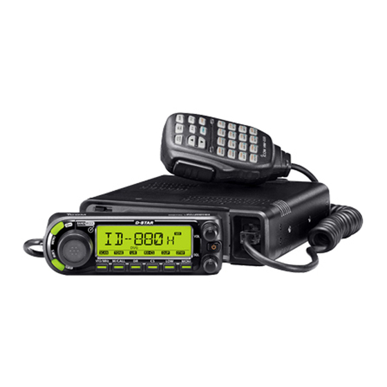
Icom ID-880H Service Manual
Vhf/uhf digital transceiver
Hide thumbs
Also See for ID-880H:
- Instruction manual (36 pages) ,
- Service manual (6 pages) ,
- Quick start manual (1 page)
Table of Contents
Advertisement
Advertisement
Table of Contents

Related Manuals for Icom ID-880H


Summary of Contents for Icom ID-880H
- Page 1 VHF/UHF DIGITAL TRANSCEIVER S-14529XZ-C1 Apr. 2009...
- Page 2 8. READ the instructions of test equipment throughly before connecting a test equipment to the transceiver. Icom, Icom Inc. and IDOM logo are registered trademarks of Icom Incorporated (Japan) in the United States, the United Kingdom, Germany, France, Spain, Russia and/or other countries.
-
Page 3: Table Of Contents
TABLE OF CONTENTS SECTION SPECIFICATIONS SECTION INSIDE VIEWS SECTION DISASSEMBLY INSTRUCTION SECTION CIRCUIT DESCRIPITON RECEIVER CIRCUITS............4-1 TRANSMITTER CIRCUITS . - Page 4 SECTION 1. SPECIFICATIONS D TRANSMITTER D GENERAL • Modulation system • Frequency coverage Variable reactance frequency modulation (unit: MHz) <For ID-880H> GMSK reactance frequency modulation (DIgital) Version • Output power : 50/15/5 W* (approx.) U.S.A. 144–148, 430–450 118–173.995* *25/15/5 W only for the TPE version.
- Page 5 SECTION 2. INSIDE VIEWS • MAIN UNIT SQUELCH AMP (IC65) LEVEL CONVERTER (IC26) LEVEL CONVERTER ELECTRIC VR (IC1001) (IC66) RESET IC (IC23) EEPROM (IC22) AMB_3.2V REGULATOR (IC1004) AF BUFFER OP+5V REGULATOR (IC49) (IC1003) DIGITAL/ANALOG AF LINE SW MODEM (IC11) (IC1012) LEVEL CONVERTER MODULATION MUTE SWITCH (IC46)
-
Page 6: Control Unit
• CONTROL UNIT BACKLIGHT DRIVER (Q1) +5C REGULATOR (Q16) LCD CONTRAST ADJUSTER (Q15) LCD DRIVER (IC7) RESET IC (IC2) CPU CLOCK (9.8304 MHz) (X1) FRONT CPU (IC4) +5V REGULATOR (IC8) 2 - 2... -
Page 7: Main Unit
SECTION 3. DISASSEMBLY INSTRUCTION 1. REMOVING TOP AND BOTTOM COVERS 2. REMOVING THE MAIN UNIT (continued) 1) Unscrew total of 18 screws; 4 screws from the top cover, 3) Unscrew 10 screws from the MAIN UNIT. 4) Unscrew 4 screws from the chassis. 8 screws from the both sides and 4 screws from the bottom cover. -
Page 8: Receive Circuits
SECTION 4. CIRCUIT DESCRIPTION 4-1 RECEIVE CIRCUITS 800 M Hz BAND (810–999 MHz) RF CIRCUITS The RX signals (810–999 MHz) from the antenna are 144 MHz BAND (118–174 MHz) passed through the HPF, and applied to the RF AMP (Q28). The RX signals (118–174 MHz) from the antenna are The amplifi... - Page 9 1st IF CIRCUITS 2nd IF AND DEMODULATOR (for FM and AM) CIRCUITS 144 MHz BAND (118–174 MHz) The 1st IF signal from the 1st IF circuits is applied to the The RX signals (118–174 MHz) from the RF circuit are IF IC (IC15, pin 20).
- Page 10 FM DEMODULATOR CIRCUITS AF FILTER CIRCUITS In the FM mode, the filtered 2nd IF signal input from The demodulated AF signals are applied to the AF filter pin 7 is amplified by the internal limiter amplifier, and FM- (Q47) via the digital/analog signal selector (IC11), to obtain demodulated at the internal quadrature detector.
-
Page 11: Transmitter Circuits
4-2 TRANSMITTER CIRCUITS TX AF CIRCUITS The MIC signals from the AF SW (IC52) are passed through MIC signals from the connected microphone are passed the pre-emphasis and IDC (for amplitude-limitting) circuits through the HPF (Q87), and amplified by the MIC AMP (IC48b), MIC level adjustment circuit (IC48a) and the (IC28). - Page 12 TX AMPLIFIER CIRCUITS (VHF BAND) TX AMPLIFIERS (UHF BAND) The output signal of VHF VCO (Q111, D145–148) is passed The output signal of UHF VCO (Q73, D87, 91, 92) is passed through the LO SW (D155), LPF and ATT, then applied to through the LO SW (D103), HPF and ATT, then applied to the drive AMP (Q25) via the limiter (D29), to obtain adequate the pre-drive AMP (Q22).
-
Page 13: Frequency Synthesizer
4-3 FREQUENCY SYNTHESIZER VCOs The PLL circuit provides stable oscillation of the transmit VHF VCO frequency and receive 1st LO frequency. The PLL output The VHF VCO is composed by the oscillator circuit (Q111, frequency is controlled by control signals including divide D145, 146, 147) and buffer AMP (Q113), and generates ratio (“PLLCK,”"PLLDATA”and "PLLSTB") from the CPU both of 1st LO signals and TX signal for VHF band. -
Page 14: Cpu (Main Unit; Ic25) Port Allocation
4-4 CPU (MAIN UNIT; IC25) PORT ALLOCATION LINE NAME DESCRIPTION LINE NAME DESCRIPTION Beep, DTMF and european tone (E880 Audio response select signal. DTMF only) signals. "H"=FM mode. "L"=DV mode. MIC_SEL Connected microphone detect signal. Cut-off frequency shifting signal to the DA_SEL [UP]/[DWN] key input from connected MICUD... -
Page 15: Voltage Block Diagram
4-5 VOLTAGE BLOCK DIAGRAM Voltage from the power supply is routed to the whole of the transceiver via regulators and switches. MAIN UNIT CONTROL UNIT TX power NOISE amplifiers (IC2, IC3) FILTER IC55, D164 CPU (IC13), +3.2V IDET CURRENT CPU (IC25) Regulator (Q14, Q15), DETECT (for current monitoring) -
Page 16: Preparation
SECTION 5. ADJUSTMENT PROCEDURE 5-1 PREPARATION ¤ REQUIRED INSTRUMENTS INSTRUMENTS SPECIFIDATION INSTRUMENTS SPECIFIDATION DC Cable (Supplied with transceiver) JIG cable (See the illust below) Output voltages : 13.8 V DC Input impedance : 50 kΩ Power Supply and 12.0 V DC Multimeter Measuring range : 0.1–20V/0.01–5 A... - Page 17 M CONNECTION Oscilloscope Modulation analyzer RF power meter Standard signal generator (DC measurable) 60 W Except [TPE] –127 to –17 dBm 30 W [TPE] (0.1 V to 32 mV) Attenuator Frequency 40 dB or 50 dB counter CAUTION: DO NOT transmit while to the antenna connector SSG is connected to the antenna connector.
-
Page 18: Frequency And Transmit Amplifier Adjustments
5-2 FREQUENCY AND TRANSMIT AMPLIFIER ADJUSTMENT Select an adjustment item using [VFO/MHz] / [M/CALL], then set the adjustment value as specifi ed using [DIAL]. ADJUSTMENT ADJUSTMENT OPERATION VALUE ITEM REFERENCE 1) Connect an RF power meter to the antenna connector. 2) Loose couple a frequency counter to the antenna FREQUENCY 435.0000 MHz... -
Page 19: Analog Deviation Adjustments (Vhf Band)
5-3 ANALOG DEVIATION ADJUSTMENTS (VHF BAND) Select an adjustment item using [VFO/MHz] / [M/CALL], then set the adjustment value as specifi ed using [DIAL]. ADJUSTMENT ADJUSTMENT OPERATION VALUE ITEM VHF BAND 1 1) Connect a modulation analyzer to the antenna connector through an attenuator, and set is as;... -
Page 20: Analog Deviation Adjustments (Uhf Band)
5-4 ANALOG DEVIATION ADJUSTMENTS (UHF BAND) Select an adjustment item using [VFO/MHz] / [M/CALL], then set the adjustment value as specifi ed using [DIAL]. ADJUSTMENT ADJUSTMENT OPERATION VALUE ITEM UHF BAND 1 1) Connect a modulation analyzer to the antenna connector through an attenuator, and set is as;... -
Page 21: Digital Deviation Adjustment
5-5 DIGITAL DEVIATION ADJUSTMENT Select an adjustment item using [VFO/MHz] / [M/CALL], then set the adjustment value as specifi ed using [DIAL]. ADJUSTMENT ADJUSTMENT OPERATION VALUE ITEM VHF BAND 1 • Connect a modulation analyzer to the antenna connector DV DEVIATION through an attenuator, and set is as;... -
Page 22: Receive Sensitivity Adjustment
5-6 RECEIVE SENSITIVITY ADJUSTMENT 1) Select an adjustment item using [VFO/MHz] / [M/CALL]. 2) Set the SSG as specifi ed (frequency, deviation and output level). 3) Push [BAND] to adjust (automatic) and store the adjustment value. ADJUSTMENT ADJUSTMENT OPERATION VALUE ITEM RECEIVE 1 •... -
Page 23: S-Meter Adjustment
5-7 S-METER ADJUSTMENT 1) Select an adjustment item using [VFO/MHz] / [M/CALL]. 2) Set the SSG as specifi ed (frequency and output level). 3) Push [BAND] to adjust (automatic) and store the adjustment value. ADJUSTMENT ADJUSTMENT OPERATION VALUE ITEM S-METER 1 •... -
Page 24: Squelch Adjustment
5-7 S-METER ADJUSTMENT (continued) 1) Select an adjustment item using [VFO/MHz] / [M/CALL]. 2) Set the SSG as specifi ed (frequency and output level). 3) Push [BAND] to adjust (automatic) and store the adjustment value. ADJUSTMENT ADJUSTMENT OPERATION VALUE ITEM (Full scale) 20 •... - Page 25 SECTION 6. PARTS LIST [CONTROL UNIT] [CONTROL UNIT] PARTS PARTS DESCRIPTION DESCRIPTION LOCATION LOCATION 1110005991 S.IC S-80945CNMC-G9F-T2G 49.5/15.5 R128 7030005050 S.RES ERJ2GEJ 103 X (10K) 59.8/9.1 1140014930 S.IC UPD78F0512AGA(R)-GAM-AX 31.9/13.4 R129 7030005090 S.RES ERJ2GEJ 104 X (100K) 32/8 1130014930 S.IC LC75827W-E 69.8/24 R130...
- Page 26 [CONTROL UNIT] [MAIN UNIT] PARTS PARTS DESCRIPTION DESCRIPTION LOCATION LOCATION 2260003190 S.SWI SKQYPAE010 110.3/17.5 1110004310 S.IC M62352GP 75EC 77.4/91.7 2260003190 S.SWI SKQYPAE010 35.9/5.8 1150002122 IC S-AU82AL(I,Q) 2260003190 S.SWI SKQYPAE010 47.3/5.8 1150002162 IC S-AV32A(I2,Q) 2260003190 S.SWI SKQYPAE010 58.7/5.8 1110004050 S.IC NJM3404AV-TE1-#FMZB 49.7/37.2 2260003190 S.SWI SKQYPAE010...
- Page 27 [MAIN UNIT] [MAIN UNIT] PARTS PARTS DESCRIPTION DESCRIPTION LOCATION LOCATION 1510000581 S.TRA 2SA1362-GR(TE85R,F) 99.9/113.1 D126 1790001251 S.DIO MA2S1110GL [EUR] 64.7/97 1520000460 S.TRA 2SB1132 T100 R 92.1/119.8 1790001251 S.DIO MA2S1110GL [ITR] 1530003990 S.TRA 2SC4738-BL(TE85L,F) 91.7/115.8 1790001251 S.DIO MA2S1110GL [EUR-01] 1590002270 S.TRA UMG9NTR 119.3/48.2 D127...
- Page 28 [MAIN UNIT] [MAIN UNIT] PARTS PARTS DESCRIPTION DESCRIPTION LOCATION LOCATION 6200011660 S.COI LQW18ANR15G00D 26.3/35.5 7030005050 S.RES ERJ2GEJ 103 X (10K) 23.4/30.4 6200011670 S.COI LQW18AN82NG00D 45.3/27.1 7030007270 S.RES ERJ2GEJ 151 X (150) 81.6/45.7 6200011670 S.COI LQW18AN82NG00D 51.9/27.3 7030005090 S.RES ERJ2GEJ 104 X (100K) 42.4/9.1 6200010060 S.COI AS080647-56N...
- Page 29 [MAIN UNIT] [MAIN UNIT] PARTS PARTS DESCRIPTION DESCRIPTION LOCATION LOCATION R272 7030007280 S.RES ERJ2GEJ 331 X (330) 57.2/104.6 R465 7030005040 S.RES ERJ2GEJ 472 X (4.7K) 83.5/44.1 R276 7030005070 S.RES ERJ2GEJ 683 X (68K) 63.7/111.5 R473 7030005120 S.RES ERJ2GEJ 102 X (1K) 110.8/125.4 R277 7030007350 S.RES ERJ2GEJ 393 X (39K)
- Page 30 [MAIN UNIT] [MAIN UNIT] PARTS PARTS DESCRIPTION DESCRIPTION LOCATION LOCATION R619 7030005000 S.RES ERJ2GEJ 471 X (470) 97.8/114.5 R854 7030005110 S.RES ERJ2GEJ 224 X (220K) 56.5/39.6 R620 7030005050 S.RES ERJ2GEJ 103 X (10K) 93.5/115.8 R855 7030005310 S.RES ERJ2GEJ 124 X (120K) 43.5/41 R621 7030005160 S.RES ERJ2GEJ 105 X (1M)
- Page 31 [MAIN UNIT] [MAIN UNIT] PARTS PARTS DESCRIPTION DESCRIPTION LOCATION LOCATION R1052 7030007250 S.RES ERJ2GEJ 220 X (22) 43.2/119.6 C123 4030017590 S.CER ECJ0EC1H070C 71.4/43.6 R1053 7030005290 S.RES ERJ2GEJ 682 X (6.8K) 52.7/116.8 C124 4030017350 S.CER ECJ0EC1H020B 71.4/42.7 R1054 7030005060 S.RES ERJ2GEJ 333 X (33K) 51.8/115.6 C125 4030017350 S.CER ECJ0EC1H020B...
- Page 32 [MAIN UNIT] [MAIN UNIT] PARTS PARTS DESCRIPTION DESCRIPTION LOCATION LOCATION C251 4030017460 S.CER ECJ0EB1E102K 16.2/25.7 C415 4030017730 S.CER ECJ0EB1E471K 103.6/46.7 C254 4030017460 S.CER ECJ0EB1E102K 47.8/42.8 C416 4030017460 S.CER ECJ0EB1E102K 62.6/69.3 C255 4030017460 S.CER ECJ0EB1E102K 36.7/16.8 C418 4030017730 S.CER ECJ0EB1E471K 61.2/66.3 C260 4030017560 S.CER ECJ0EC1H2R5B 32.4/29.9...
- Page 33 [MAIN UNIT] [MAIN UNIT] PARTS PARTS DESCRIPTION DESCRIPTION LOCATION LOCATION C591 4030017460 S.CER ECJ0EB1E102K 125.3/8.7 C768 4030009570 S.CER C1608 CH 1H 0R3B-T 99.9/23.2 C592 4030017460 S.CER ECJ0EB1E102K 116.5/6 C769 4030017460 S.CER ECJ0EB1E102K 104.8/28.8 C593 4030017420 S.CER ECJ0EC1H470J 114.3/130.8 C770 4030017460 S.CER ECJ0EB1E102K 104.8/24.4 C594 4030017510 S.CER ECJ0EC1H680J...
- Page 34 [MAIN UNIT] [MAIN UNIT] PARTS PARTS DESCRIPTION DESCRIPTION LOCATION LOCATION C976 4030017420 S.CER ECJ0EC1H470J 61.8/19.5 C1092 4030016790 S.CER ECJ0EB1C103K 62/90.4 C977 4030017460 S.CER ECJ0EB1E102K 64.3/14.6 C1093 4030018920 S.CER ECJ0EB1H392K 50.3/129.4 C978 4030017620 S.CER ECJ0EC1H100C 66.3/11.7 C1094 4030016790 S.CER ECJ0EB1C103K 107.1/73.1 C979 4510008120 S.ELE 16 CE 100 BS...
- Page 35 SECTION 7. MECHANICAL PARTS [CHASSIS PARTS] [MAIN UNIT] ORDER ORDER DESCRIPTION QTY. DESCRIPTION QTY. 6510014961 B2B-ZR-SM4-TF (LF) (SN) 6510004880 MR-DSE-01 6510023110 3008L-8P8C 6510025950 PCB-606 (6P6C) 8600036881 ZHR-2 (Incl. W1, 2) 6510023161 DN-508B-6-L 6450001430 HSJ1462-01-010 2510001160 057P0802 6510014961 B2B-ZR-SM4-TF (LF) (SN) 6510025940 PJ-3047S 2710000820 EFB0412VHD-6P38 J24*...
- Page 36 • CONTROL UNIT MP18×4(CO) MP16×2(CO) MP17×2(CO) MP2(CO) MP13(CO) CONTROL UNIT S14(CO) J2(CO) MP15×2(CO) EP2(CO) J3(CO) MP6(CO) MP5(CO) MP28×2(CO) DS25(CO) MP23(CO) R3(CO) DS20(CO) MP26×2(CO) R7(CO) MP24(CO) MP20(CO) MP4(CO) MP28×2(CO) MP21(CO) MP9(CO) MP27×6(CO) MP10(CO) MP11(CO) MP12(CO) MP8×6(C) UNIT ABBREVIATIONS; (C)= CHASSIS (CO)= CONTROL UNIT MP7(C) 7 - 2...
- Page 37 • MAIN UNIT MP15×4(C) MP21(C) SP1(C) MP3(C) MP20(C) MP6(C) MP16×4(C) MP7(C) MP19×2(C) MP11(C) MP14×2(C) MP8(C) MP2(C) MP15×4(C) MF1(C) MP12(C) J1(C) MP9(C) MP4(C) MP1(C) MP10(C) IC3(M) IC2(M) MAIN UNIT MP5(C) MP15×2(M) MP15×4(C) MP22×4(C) MP13×3(M) MP11(M) MP14×2(M) MP13×3(M) MP12(M) UNIT ABBREVIATIONS; (C)= CHASSIS (M)= MAIN UNIT MP15×4(C) MP13×10(C)
- Page 38 The combination of top side and bottom side of this SECTION 8. BOARD LAYOUTS • MAIN UNIT (TOP VIEW) EP52 R521 R883 R893 R522 R523 C679 IC65 D165 Q102 R642 C617 C689 R920 EP53 R906 D167 IC1001 C959 EP16 R626 EP18 R908 R476...
- Page 39 The combination of top side and bottom side of this • MAIN UNIT (BOTTOM VIEW) IC38 R508 EP39 R835 EP66 R830 EP40 R836 R489 EP57 C1069 EP58 [EXTERNAL C616 C709 R815 C594 R481 EP25 D161 SPEAKER JACK] EP35 EP19 C914 C943 TDATA IC1000...
- Page 40 SECTION 9. BLOCK DIAGRAM Q1010 2SC4738 FANH V Q87: IC28: IC30: IC29: IC52: IC48 1/4,2/4: IC51: J201 5 2SC4738 TA75S558 Q 88:UNR9213 CD4066 TC7W53 TC7W53 LM2902 TC7W53 From the microphone MIC SENS AMOD MAIN UNIT AM P MUT E SELECT I C55:ZXCT1022 D163,D164:MA2S1110G IC48 4/4:...
- Page 41 Q110:UNR9214 Q 15:2SA1362 Q 12:UNR9213 VCO_SHIFT SHIFT D59:L709CE Q 111:2SC5231A VCO8 VTX_C D39,D47,D1005 D68,D75:HVU131 D 145,D146,D147 MA2S1110G MT3S20P S-AV32 MA742 D77:HSC277 I C42:TC7S66 HVC327C VHFYGR Q121:UNR9213 D148:HSC277 D160,D175 LO SW DRIVE PW R TX/RX Q113:2SC5231A LIMITER AM P AM P VHF VCO :HSC277 AMOD...
- Page 42 SECTION 10. VOLTAGE DIAGRAM CONTROL UNIT GREEN_D1 GREEN :5.7 R125 YERROW:6. 3 GREEN_D2 AMBER :7.9 GREEN_D3 GREEN_D4 2SC4738 2SC4738 2SC4738 2SC4738 RED_D1 GREEN :5.7 RED_D2 YERROW:6. AMBER :7.9 RED_D3 RED_D4 2SC4738 2SC4738 2SC4738 2SC4738 6.05 DS20 TAK-43542 4. 3 2SA1586 2SC4738 0.
- Page 43 MAIN UNIT (1/7) TX;7. 8 RX;0.0 C;7. 9 C H A S S I S VHF TX:4. 9 J 2 1 I C3 RX:0. 0 S-AV32A VTX_C AS080647 AS080547 AS080647 UNR9213G0 AS080647 AS080547 L 46 L 56 L 88 L 9 2 L 96 0 .
- Page 44 MAIN UNIT (2/7) FANHV DA_STB DA_CK M PZ1608S221A DA_DAT A E P 1 I C1 FAST:11. 5 MID: 9.5 SLOW: 7.8 FANCONT C H A S S I S u n i t MMZ1608Y102BT Q123 EP 7 1 2SB1132 MF 1 AO12 2SC4738 AO10...
- Page 45 MAIN UNIT (3/7) FANHV FANHV VHFYGR MOD_DA TX:4. 9 PLLCK MOD_DA To MAIN UNIT RX:0. 0 PLLDATA VHFYGR (6/7) PLLSTB 300_R5 300_R5 VTX_C VTX_C LMV321IDCK C;4. 9 R810 C;7. 9 IC53 UTX_C UTX_C VTX_C VTX_C 100K UTX_C 140_R5 UTX_C 140_R5 800_R5 800_R5 R808...
- Page 46 MAIN UNIT (4/7) FANHV FANH V R1053 C ; 4 .9 MA2S1110G 6.8K R1054 D1002 2SA1586 Q1008 2SC4116 I C101 6 Q1009 R1056 R1085 C680 SN74LVC2GU04DCKR IC38 M PZ1608S221A Q1010 4.7K R639 M PZ1608S221A C679 2SC4738 C709 EP52 IC66 0.047 R631 VIN1 VIN2...
- Page 47 MAIN UNIT (5/7) FANHV R917 R926 0.006 R918 Q126 ZXCT1022 0.006 R850 2SB1132 VOUT LOAD IC24 OPC-465 C847 2SB1132 TA7808F IC55 C ; 7 .9 CTH30V222S15A C ; 4 .9 C ; 4 .9 AVR-M1005C270M R477 2SA1588 R498 MA2S1110G MA2S1110G 2.2K D1003 C1073...
- Page 48 MAIN UNIT (6/7) PLLSW C;7.9V VCO8 0.001 C446 300_R5 VHF;7.0 Q121 HSC277TRF R455 R460 R848 L131 L134 D180 UNR9213G0 D104 1SV308 MMUTE C771 UNR9213G0 VCO_SHIFT R695 R713 R694 R696 R697 L144 R702 0.001 0.47U 1.5K 1.2K 1.2K Q111 8.2K R364 100K C770 D160...
- Page 49 MAIN UNIT (7/7) D V : 1 . 3 V FM:0V R1029 C1050 R1028 D V : 3 . 2 V 150K R1037 R1032 FM:0V Q1005 2SC4738 C1044 D V : 0 . 4 V 0.001 FM:0V R1024 D V : 4 . 7 V Q1003 C1039 F M : 0 .
- Page 50 Phone : +81 (06) 6793 5302 F ax : +81 (06) 6793 0013 : http://ww w .icom.c o .jp/ w o r ld/ind e x.html <Co r po r ate Headqua r ters> Communication Equipment 2380 116th A v e n ue N.E., Bell e vu e , W A 98004, U . S .A.
- Page 51 S-14529XZ-C1 1-1-32, Kamiminami, Hirano-ku, Osaka 547-0003, Japan © 2009 Icom Inc.
Need help?
Do you have a question about the ID-880H and is the answer not in the manual?
Questions and answers