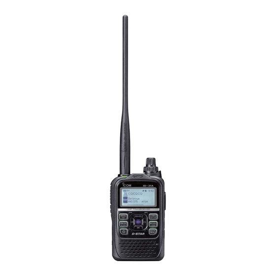
Icom ID-31A Service Manual
Hide thumbs
Also See for ID-31A:
- Instruction manual (80 pages) ,
- Advanced instructions (293 pages) ,
- Quick manual (2 pages)
Table of Contents
Advertisement
Quick Links
Advertisement
Table of Contents

Related Manuals for Icom ID-31A


Summary of Contents for Icom ID-31A
- Page 1 UHF TRANSCEIVER S-14813XZ-C1 Feb. 2012...
- Page 2 8. READ the instructions of the test equipment throughly before connecting it to the transceiver. Icom, Icom Inc. and the Icom logo are registered trademarks of Icom Incorporated (Japan) in Japan, the United States, the United Kingdom, Germany, France, Spain, Russia and/or other countries.
-
Page 3: Table Of Contents
TABLE OF CONTENTS SECTION SPECIFICATIONS SECTION INSIDE VIEWS SECTION DISASSEMBLY INSTRUCTION SECTION CIRCUIT DESCRIPITON RECEIVER CIRCUITS............4-1 TRANSMITTER CIRCUITS . -
Page 4: Specifications
: More than 0.4 W with a 16 Ω load • Power supply : 10.0–16.0 V DC for external DC power, Internal speaker or specifi ed Icom’s battery pack : More than 0.2 W with a 8 Ω load External speaker • Digital transmission speed : 4.8 kbps •... - Page 5 SECTION 2. INSIDE VIEWS • LOGIC UNIT (TOP VIEW) RX/TX LED DRIVER (Q24) +3.3 V REGULATOR (IC11) BACKUP BATTERY MIC/VOX AMP (For the real time clock) (IC19) (BT1) 2 - 1...
- Page 6 • LOGIC UNIT (BOTTOM VIEW) CLOCK OSCILLATOR (For the CPU) (X2) GPS MODULE CONTROLLER (IC5) (IC1) EEPROM (For the CPU) (IC7) DATA LEVEL CONVERTER (IC21) CLOCK OSCILLATOR (For the DSP) EEPROM (For GPS data) (X3) (IC3) (IC18) SERIAL DATA INTERFACE SERIAL FLASH MEMORY (IC2) (IC20)
- Page 7 • MAIN UNIT (TOP VIEW) CURRENT DETECTION IC (IC5) VCC LINE SW (Q2) VCC LINE SW (Q8) +5 V REGULATOR (IC1) POWER AMP (Q45) DRIVE AMP (Q41) 2ND IF FILTER (For FM mode) (FI2) CHARGING LINE SW (Q39) (Q7) 2ND IF FILTER LOCK VOLTAGE BUFFER (For DV/FM-N mode) (Q26)
- Page 8 • MAIN UNIT (BOTTOM VIEW) RF AMP (Q47) 1ST IF MIXER (Q46) 1ST IF FILTER TX POWER SETTING (FI3) VOLTAGE BUFFER (IC14) AF POWER AMP (IC2) BPF TUNING VOLTAGE BUFFER CHARGING LINE DRIVER (IC12) (Q6) (IC6) IF IC (IC13) +4 V REGULATOR AF LINE SW (IC3) (IC8)
- Page 9 1) Remove 2 dials and antenna nut from the front panel. 5) Unsolder 6 points at the rotary encoder. Inner dial UNSOLDER Antenna nut Screws x5 Outer dial Remove with; “ICOM Driver (Q)” Solder (8960000370) remover LOGIC UNIT 2) Remove 2 screws from the bottom of chassis. Screws Rotary encoder...
- Page 10 2. REMOVING THE MAIN UNIT 3) Unsolder a point at the antenna connector. 1) Unsolder 3 points on the shield plate. UNSOLDER UNSOLDER Solder remover Solder remover 2) Remove 5 screws from the shield plate, and then 4) Remove 6 screws from the MAIN UNIT, and then remove it.
-
Page 11: Circuit Descripiton
SECTION 4. CIRCUIT DESCRIPTION 4-1 RECEIVE CIRCUITS RF CIRCUITS (MAIN UNIT) RX AF CIRCUITS (MAIN AND LOGIC UNITS) The RX signal from the antenna is passed through two LPFs • While operating in the DV mode (L32, L34, C302, C303, C306, C307, C312 and L29, C281, The demodulated AF signal is passed through the LPF (MAIN C285), ANT SW (D24, D25, D31, D33, L36, C313, C315, UNIT: R118, R121, C122, C130, C135), and then applied to... -
Page 12: Transmitter Circuits
4-2 TRANSMIT CIRCUITS TX AF CIRCUITS (LOGIC AND MAIN UNITS) • When operating in the FM/FM-N mode The amplifi ed signal is passed through the MIC mute SW The AF signal from the internal or external microphone (MIC (LOGIC UNIT: IC16, pins 1, 7), and then applied to the MAIN signal) is applied to the MIC AMP (LOGIC UNIT: IC19B, pin 5). -
Page 13: Frequency Synthesizer Circuits
4-3 FREQUENCY SYNTHESIZER (MAIN UNIT) • VCO • PLL The ID-31A/E has a VCO (Q27, D10–D12) which generates A portion of VCO output signal is passed through two buffers both the 1st LO signal and the TX signal. The output of buffer (Q29 and Q30) and LPF (L7, C137–C139, C144), and then... -
Page 14: Port Allocations
4-5 PORT ALLOCATIONS • CPU (LOGIC UNIT: IC5) BALL LINE BALL LINE DESCRIPTION DESCRIPTION NAME NAME LCD and key backlight (DS1, DS3) driver GPS module (CHASSIS: EP1) controller LIGHT (Q23) control. G_RES (IC1) reset. L: Reset. LCD backlight (DS1, DS3) dimmer control. H: Blight. - Page 15 • CPU (LOGIC UNIT: IC5) (Continued) • D/A CONVERTER (MAIN UNIT: IC11) LINE BALL LINE DESCRIPTION DESCRIPTION NAME NAME Tuning voltage to the BPF (D32, L40, DSP_SI DSP (IC10) serial data. BPF1 C353). DSP_ DSP (IC10) “AFC” input. Tuning voltage to the BPF (D27, D29, D30, AFC1 BPF3 L28, L31, L33, C286, C290, C292, C293,...
-
Page 16: Adjustment Procedures
SECTION 5. ADJUSTMENT PROCEDURE 5-1 PREPARATION ¤ REQUIRED EQUIPMENTS EQUIPMENT GRADE AND RANGE EQUIPMENT GRADE AND RANGE Voltage range : 1–15 V Modifi ed 3-conductor plugs Power supply JIG cable Current capacity : More than 3 A (See the illustration below) Audio generator Frequency range : 300–3000 Hz... - Page 17 • ENTERING THE ADJUSTMENT MODE 1) Connect the JIG cable “#1” (See page 5-1) to [SP]. 2) While holding down [SQL] and , turn ON the power. Connect the JIG cable “#1” (See page 5-1) here. [SQL] Push to turn ON the power. [QUICK/MENU] •...
-
Page 18: Frequency Adjustment
5-2 FREQUENCY ADJUSTMENT Select an adjustment item using , and then set the adjustment value as specifi ed using [DIAL]. ADJUSTMENT ADJUSTMENT OPERATION VALUE ITEM REFERENCE 1) Set the power supply voltage to 7.4 V. FREQUENCY 2) Connect a power meter or dummy load to the antenna connec- Displayed tor. - Page 19 5-3 TRANSMIT ADJUSTMENT (Continued) • IDLING CURRENT ADJUSTMENT (at 13.5 V) Select an adjustment item using , and then set the adjustment value as specifi ed using [DIAL]. ADJUSTMENT ADJUSTMENT OPERATION VALUE ITEM DRIVE AMP 1 1) Set the power supply voltage to 13.5 V. (supplying from [DC IN]) IDLING CURRENT 2) Connect an RF power meter to the antenna connector.
- Page 20 5-3 TRANSMIT ADJUSTMENT (Continued) • TRANSMIT POWER ADJUSTMENT (at 13.5 V) Select an adjustment item using , and then set the adjustment value as specifi ed using [DIAL]. ADJUSTMENT ADJUSTMENT OPERATION VALUE ITEM TRANSMIT POWER 1 1) Set the power supply voltage to 13.5 V. (supplying from [DC IN]) –...
- Page 21 5-3 TRANSMIT ADJUSTMENT (Continued) • TONE DEVIATION ADJUSTMENTS Select an adjustment item using , and then set the adjustment value as specifi ed using [DIAL]. ADJUSTMENT ADJUSTMENT OPERATION VALUE ITEM TONE DEVIATION 1 1) Set the power supply voltage to 7.4 V. 2) Connect a modulation analyzer to the antenna connector through an attenuator, and then set it as;...
-
Page 22: Receive Adjustment
5-4 RECEIVE ADJUSTMENTS 1) Select an adjustment item (band) using 2) Set the SSG as specifi ed (frequency, deviation and output level), and then push to automatically adjust. ADJUSTMENT ADJUSTMENT OPERATION VALUE ITEM RECEIVE NOTE: “RECEIVE SENSITIVITY” must be adjusted before “S-METER.” Otherwise, “S-METER” will SENSITIVITY not be adjusted properly. -
Page 23: Parts List
SECTION 6. PARTS LIST [MAIN UNIT] [MAIN UNIT] PARTS PARTS DESCRIPTION DESCRIPTION LOCATION LOCATION 1110007860 S.IC S-80950CLPF-G7LTFG 19.2/31.95 1750000711 S.VAR HVC350BTRF-E 17.6/39.7 1110007610 S.IC TPA0211DGNR 36.3/39.5 1750001820 S.DIO LRB706F-40T1G <SLVJ> 13.2/10.0 1180003800 S.REG NJU7775F04-TE2-#ZZZB 31.6/32.6 1750000711 S.VAR HVC350BTRF-E 14.2/41.6 6910022360 S.DC TPS62110RSAR 81.8/12.7 1750000711 S.VAR... -
Page 24: Main Unit
[MAIN UNIT] [MAIN UNIT] PARTS PARTS DESCRIPTION DESCRIPTION LOCATION LOCATION 7030012270 S.RES ERJ2RKD 1203X (120K) 13.8/14.2 R169 7030005220 S.RES ERJ2GEJ 223 X (22K) 39.9/7.5 7030005160 S.RES ERJ2GEJ 105 X (1M) 68.8/14.1 R170 7030008010 S.RES ERJ2GEJ 123 X (12K) 50.9/42.2 7030005290 S.RES ERJ2GEJ 682 X (6.8K) 45.6/19.0 R171 7030005060 S.RES ERJ2GEJ 333 X (33K) - Page 25 [MAIN UNIT] [MAIN UNIT] PARTS PARTS DESCRIPTION DESCRIPTION LOCATION LOCATION 4030017460 S.CER C1005 JB 1H 102K-T 52.8/41.1 Eqv. 4550008160 S.TAN F931A226MAA 4030017350 S.CER C1005 CH 1H 020B-T 13.9/22.7 C122 4030018820 S.CER C1005 JB 1H 561K-T 60.4/31.7 4030017460 S.CER C1005 JB 1H 102K-T 15.5/35.4 C123 4030017910 S.CER C1005 JB 1H 152K-T...
- Page 26 [MAIN UNIT] [MAIN UNIT] PARTS PARTS DESCRIPTION DESCRIPTION LOCATION LOCATION C237 4030017460 S.CER C1005 JB 1H 102K-T 32.5/18.3 6450000870 CON HEC2711-01-020 C238 4030016790 S.CER C1005 JB 1E 103K-T 47.3/33.7 6510028130 S.CON AXK5S50047YG 66.5/37.2 C240 4030016790 S.CER C1005 JB 1E 103K-T 49.3/29.7 6510025880 CON TC38-108-01 <CFE>...
-
Page 27: Logic Unit
[LOGIC UNIT] [LOGIC UNIT] PARTS PARTS DESCRIPTION DESCRIPTION LOCATION LOCATION 1190003230 S.IC FGS4ER-PX-112 18.2/24.1 7030008400 S.RES ERJ2GEJ 182 X (1.8K) 33.5/38.0 1120003020 S.IC MAX3221IPWR 35.5/37.4 7030008400 S.RES ERJ2GEJ 182 X (1.8K) 33.5/37.1 1140015870 S.IC M24M01-RMN6TP 61.0/5.8 7030005090 S.RES ERJ2GEJ 104 X (100K) 33.5/35.3 1130015740 S.IC S-35390A-I8T1G... - Page 28 [LOGIC UNIT] [LOGIC UNIT] PARTS PARTS DESCRIPTION DESCRIPTION LOCATION LOCATION R151 7030005240 S.RES ERJ2GEJ 473 X (47K) 64.6/28.6 R272 7030005090 S.RES ERJ2GEJ 104 X (100K) 33.5/11.0 R152 7030005120 S.RES ERJ2GEJ 102 X (1K) 49.1/24.7 R273 7030012260 S.RES ERJ2RKD 4703X (470K) 16.3/7.2 R153 7030010040 S.RES ERJ2GEJ-JPW...
- Page 29 [LOGIC UNIT] [LOGIC UNIT] PARTS PARTS DESCRIPTION DESCRIPTION LOCATION LOCATION C114 4030017460 S.CER C1005 JB 1H 102K-T 57.8/34.1 C511 4030017440 S.CER C1005 CH 1H 221J-T 53.7/17.5 C115 4030018890 S.CER C1005 JB 0J 224K-T 48.6/34.2 C512 4030017440 S.CER C1005 CH 1H 221J-T 45.5/16.3 C116 4030019120 S.CER GRM188B31E105KA75D...
- Page 30 SECTION 7. MECHANICAL PARTS [CHASSIS PARTS] [LOGIC UNIT] ORDER ORDER DESCRIPTION QTY. DESCRIPTION QTY. 6510025970 41-002AA-R <MRF> 6910015630 2682 ANT CONNECTOR <EIK> 6510028080 27FHSY-RSM1-GAN-TB (LF) (SN) 6510028170 SDHL-8BNS-K-363-A0-ETB (HF) 6510024580 HSJ1621-019011 2510001650 K028NA510-13 <OSC> 6510027760 AXK6S50547YG 3310004270 AGA121204-S0-A6 <MRF> DS10 5030003520 BTG-12864ET-FBWD-N-G-A2 <VKHK>...
- Page 31 MP37(C) MP27(C) J1(C) EP1(C) GPS module MP16(C) MP56(C) To J1(L) MP26(C) MP21(C) (Bottom view) MP1(C) MP19(C) MP42(C) S12(L) MP38(C) MP52(C) MP33(C)×2 MP30(C)×6 MP35(C) MP54(C) MP22(C) MP53(C) MP50(C) MP30(C)×5 MAIN UNIT MP18(C) MP1(M) MP28(C) MP30(C)×5 MP48(C) J1(L) MP48(C) MP7(C) MP12(C) MP23(C) MP8(C) MP39(C)×2 LOGIC UNIT...
- Page 32 SECTION 9. BOARD LAYOUTS The combination of this page and next page shows the top side and bottom side of actual P.C. board. • MAIN UNIT • LOGIC UNIT [ANT] (TOP VIEW) (TOP VIEW) MP28 C208 C107 R109 R108 [MIC] –...
- Page 33 [DIAL/VOL] • LOGIC UNIT • MAIN UNIT The combination of this page and next page shows the top side and bottom side of actual P.C. board. (BOTTOM VIEW) (BOTTOM VIEW) R108 R107 C335 C102 R265 C320 C316 C324 C503 R280 To EP1 (CHASSIS) C353 C326...
- Page 34 SECTION 10. BLOCK DIAGRAM BTL5V AFON CLONE MAIN UNIT CHASSIS UNIT EXTMIC D_AS FMMUTE BUFF IC16 IC16 MMUTE MODE BPF1,BPF2 BPF3,SQLOUT IC8,Q22 IC9A IC9D IC19B VCOMOD VCOMOD BUFF MMUTE PLAY IC15 DMOD REFMOD REFMOD IC14 IC12B LINEAR RTONE CODEC IC12A REFCON REFCON PWDAN...
- Page 35 VCO_MUTE MUTE VCC-I VCO3 VCOMOD DRIVE BUFF BUFF 3VS,+5V D13,D14 D20,D21 D24,D25 Q27,D10,D11,D12 D31,D33 TTEMP D26,D28 UNLK IC14B IC12 IC14A LOOP TEMP FILTER GATE GATE CTRL CTRL CTRL PSET ISET1 ISET2 PLLDATA VCOMOD PLLCK PLLSTB MUTE REFMOD REFMOD 15.3MHz LV DET REFCON REFCON TXMUTE...
- Page 36 SECTION 11. VOLTAGE DIAGRAM • LOGIC UNIT (1/2) G_VDD 100P C501 3.27V LDTC144EE 3.31V BLED 3.29V R105 3.31V 1.82V 0.0039 1.82V R101 100k LDTC144EE 2SA1832 L1SS400 CL-165HR LDTC144EE 2SC4738 3.29V 0.01 INT1 TEMP XOUT 1.78V TX:3.29V R104 SN74LVC2GU04DCKR ON:3.29V RX:0V Busy:3.29V 2.63V INT2...
- Page 37 • LOGIC UNIT (2/2) BLM18RK102SN1 R156 IC11 EP12 3.3V_VDD MMZ1005S601CT 4.63V 3.31V 3.31V 3.30V TLV70033DDCR R188 CPU3 3.29V R284 BLM18RK102SN1 NFM18PC104R1C3 100k EP10 C129 +3.3V_A 3.30V C110 R121 150k R178 R187 DSP_ TRST 1.37V 100k IC10 R281 CVDD_1.35V CVDD_1.35V CLKOUT CLKOUT ADJ2 PFMC...
- Page 38 3.18V VCOMOD • MAIN UNIT (1/2) 3.18V 3.18V 3.27V 2SA1832 6.8K 3.18V 8.2K 0.01 2.95V C103 C119 1.87V 4.61V 0.3P 4.69V 4.01V 3.27V 2SC5006 NJU7775F04 2SC4738 LDTC144EE VOUT C132 R126 NOIS C154 0.5P 2.93V RSSI 1.5K MLG1608S CTRL 1.2K 1.8K 2.85V DMOD CHGH...
- Page 39 • MAIN UNIT (2/2) TTEMP EP16 R220 MPZ1608S101A NTCG10 7.23V C242 VCC-I C251 EP14 0.001 C200 MMZ2012Y102B 2SA1832 0.001 C216 0.40-1.5-5TL 0.001 R176 4.61V C272 C298 J500 0.40-0.9-2TL 0.001 HVD144A 0.40-0.9-2TL 0.30-0.9-5TL 0.30-0.9-6TR 0.40-0.9-2TL 0.001 ELJRE R163 TX:1.48V C307 T3C_INV R186 0.5P C197...
- Page 40 Highway 17 Delta, B.C., V4K 5B8, Canada : http://www.icomspain.com Phone : +1 (604) 952-4266 Fax : +1 (604) 952-0090 E-mail : icom@icomspain.com : http://www.icomcanada.com E-mail : info@icomcanada.com Blacksole House, Altira Park, Herne Bay, Kent CT6 6GZ, UK Phone : +44 (01227) 741741...
- Page 41 S-14813XZ-C1 1-1-32, Kamiminami, Hirano-ku, Osaka 547-0003, Japan © 2012 Icom Inc.
Need help?
Do you have a question about the ID-31A and is the answer not in the manual?
Questions and answers