Yamaha 01v 96 Service Manual
Digital mixing console
Hide thumbs
Also See for 01v 96:
- Owner's manual (36 pages) ,
- Manual (34 pages) ,
- Supplementary manual (1 page)
Table of Contents
Advertisement
Quick Links
This document is printed on chlorine free (ECF) paper with soy ink.
PA
011680
200304-250000
DIGITAL MIXING CONSOLE
SERVICE MANUAL
CONTENTS
CIRCUIT DIAGRAM
................................................... 4
.......................................................... 12
.................................. 13
............................ 23
............................................ 32
................................ 33
.................................. 41
....................................... 46
....................................................... 76/83
....................... 114
................................... 119
............................ 134
1.329K-1933
01V96
............... 21
... 90/102
.... 115/117
.......... 119
............... 120
HAMAMATSU, JAPAN
1
Printed in Japan '03.03
Advertisement
Table of Contents

Related Manuals for Yamaha 01v 96


Summary of Contents for Yamaha 01v 96
- Page 1 01V96 DIGITAL MIXING CONSOLE SERVICE MANUAL CONTENTS SPECIFICATIONS ........... 4 DIMENSIONS ............12 PANEL LAYOUT ........13 CIRCUIT BOARD LAYOUT ....21 DISASSEMBLY PROCEDURE ......23 INSTALLING AN OPTIONAL CARD ..........32 LSI PIN DESCRIPTION ........ 33 IC BLOCK DIAGRAM ........
- Page 2 IMPOR TANT NOTICE This manual has been provided for the use of authorized Yamaha Retailers and their service personnel. It has been assumed that basic service procedures inherent to the industry, and more specifically Yamaha Products, are already known and under- stood by the users, and have therefore not been restated.
- Page 3 01V96 LITHIUM BATTERY HANDLING This product uses a lithium battery for memory back-up. WARNING : Lithium batteries are dangerous because they can be exploded by improper handling. Observe the following pre- cautions when handling or replacing lithium batteries. Leave lithium battery replacement to qualified service personnel. Always replace with batteries of the same type.
-
Page 4: Specifications
01V96 SPECIFICATIONS General Spec Number of scene memories Internal 44.1 kHz, 48 kHz, 88.2 kHz, 96 kHz Sampling Frequency Normal rate: 44.1 kHz–10% to 48 kHz+6% External Double rate: 88.2 kHz–10% to 96 kHz+6% fs=48 kHz Less than 1.6 ms CH INPUT to STEREO OUT Signal Delay fs=96 kHz Less than 0.8 ms CH INPUT to STEREO OUT... - Page 5 01V96 Digital Input (2TR IN DIGITAL, ADAT input) Option Input (SLOT) Available cards Optional digital interface cards (MY16, MY8, MY4 series) Input patch — Phase Normal/reverse On/off Gate-type Key in: 12 ch Group (1–12, 13–24, 25–32)/AUX1–8 On/off Comp-type Key in: self /Stereo Link Pre EQ/pre fader/post fader Attenuator –96.0 to +12.0 dB (0.1 dB step)
- Page 6 01V96 24-bit linear, 128-times oversampling (@fs=44.1, 48 kHz), 64-times over- MONITOR OUT DA converter sampling (@fs=88.2, 96 kHz) STEREO, BUS1–8, AUX1–8, DIRECT OUT 1–32, INSERT OUT (CH1–32, Output patch BUS1–8, AUX1–8, STEREO), CASCADE OUT (BUS1–8, AUX 1–8, STEREO, OMNI OUT 1–4 SOLO) 24-bit linear, 128-times oversampling (@fs=44.1, 48 kHz), 64-times over- DA converter...
- Page 7 01V96 On/off Comp-type Pre EQ/pre fader/post fader Attenuator –96.0 to +12.0 dB (0.1 dB step) 4-band PEQ On/off AUX1–8 On/off — Fader 100 mm motorized Delay 0–29100 samples Displayed on LCD Metering Peak hold on/off Number of 4@44.1kHz, 48kHz effects 2@88.2kHz, 96kHz Bypass On/off...
- Page 8 01V96 Gate Parameters Threshold –54 dB–0 dB (0.1 dB step) Range –70 dB–0 dB (1 dB step) Attack 0 ms–120 ms (1 ms step) 0.02 ms–1.96 s (216 points) @ 48 kHz 0.02 ms–2.13 s (216 points) @ 44.1 kHz Hold Gate 0.01 ms–981 ms (216 points) @ 96 kHz...
- Page 9 01V96 Threshold –54 dB to 0 dB (0.1 dB step) Ratio (x :1) x=1, 1.1, 1.3, 1.5, 1.7, 2, 2.5, 3, 3.5, 4, 5, 6, 8, 10, 20 (15 points) Out gain –18 dB to 0 dB (0.1 dB step) Width 1 dB–90 dB (1 dB step) Compander H...
-
Page 10: Analog Input Spec
01V96 Analog Input Spec Input level Actual Load For Use With Input GAIN Connector Max. Impedance Nominal Nominal Sensitivity before clip –70 dB –60 dB –40 dB –60 dB (0.245 mV) (0.775 mV) (7.75 mV) A: XLR-3-31 type 50–600 Ω INPUT A/B –26 dB –16 dB... -
Page 11: Digital Input Spec
Digital I/O MY8-AE 44.1/48 kHz 24 bit Sampling Rate Con- MY8-AE96S AES/EBU 44.1/48/88.2/96 kHz verter for input MY8-AE96 44.1/48/88.2/96 kHz Yamaha MY4-AD — — 44.1/48 kHz MY8-AD — — 20 bit 44.1/48 kHz ANALOG IN MY8-AD24 —... -
Page 12: Top View
01V96 Control I/O Spec I/O Port Format Level Connector in Console TO HOST USB 0 V–3.3 V B type USB connector MIDI — DIN Connector 5P MIDI MIDI — DIN Connector 5P THRU MIDI — DIN Connector 5P TTL/75 Ω —... -
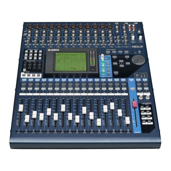
Page 13: Panel Layout
01V96 PANEL LAYOUT Control Panel AD Input Section (p. 14) SCENE MEMORY Section (p. 17) CH1-4 CH5-8 CH9-12 PHANTOM +48V Monitor Out DISPLAY ACCESS & Head- INPUT Section (p. 16) (BAL) -10dBV (UNBAL) phones Sec- PHONES INSERT OUT IN tion (p. 14) (UNBAL) CH15/16 MONITOR... - Page 14 01V96 AD Input Section CH1-4 INPUT (BAL) INSERT OUT IN (UNBAL) CH15/16 2TR IN INSERT I/O INSERT I/O INSERT I/O INSERT I/O INSERT I/O NSERT I/O INSERT I/O INSERT I/O INSERT I/O 20dB 20dB 20dB 20dB 20dB 20dB 20dB 20dB 20dB GAIN GAIN...
- Page 15 01V96 Channel Strip Section SOLO q [SEL] buttons w [SOLO] buttons e [ON] buttons r Channel faders STEREO Section q [SEL] button w [ON] button e [STEREO] fader STEREO...
- Page 16 01V96 ST IN Section ST IN q [ST IN] button w [SEL] buttons e [SOLO] buttons SOLO SOLO r [ON] buttons t Level controls ST IN 1 ST IN 2 FADER MODE Section FADER MODE q [AUX 1] - [AUX 8] buttons w [HOME] button HOME (METER) DISPLAY ACCESS Section...
- Page 17 01V96 Display Section OVER STEREO q Display w Stereo meters e Contrast control r [F1]-[F4] buttons t Left Tab Scroll [ ] button y Right Tab Scroll [ ] button SELECTED CHANNEL Section SELECTED CHANNEL q [PAN] control w [HIGH] button EQUALIZER e [HIGH-MID] button r [LOW-MID] button...
- Page 18 01V96 USER DEFINED KEYS Section USER DEFINED KEYS q [1]-[8] buttons Data Entry Section q Parameter wheel w [ENTER] button e [DEC] & [INC] buttons r Left, Right, Up, Down ] / [ ] / [ ] / [ cursor buttons ENTER SOLO Section q [SOLO] indicator...
- Page 19 01V96 Rear Panel PHANTOM +48V (p. 19) AD Output Section (p. 19) Digital I/O Section (p. 20) MIDI/Control Section (p. 20) Power Section (p. 20) SLOT Section (p. 20) PHANTOM +48V q [CH1-4 ON/OFF] switch w [CH5-8 ON/OFF] switch e [CH9-12 ON/OFF] switch AD Output Section q [MONITOR OUT] connectors L/R w [OMNI OUT] connectors 1-4...
- Page 20 01V96 Digital I/O Section q [WORD CLOCK OUT] connector w [WORD CLOCK IN] connector e [ADAT IN/OUT] connectors r [2TR OUT DIGITAL COAXIAL] connector t [2TR IN DIGITAL COAXIAL] connector MIDI/Control Section q [MIDI IN/THRU/OUT] ports w [TO HOST USB] port SLOT Section q [SLOT] Power Section...
-
Page 21: Circuit Board Layout
01V96 CIRCUIT BOARD LAYOUT Bottom Assembly <Top view> MAIN Power Transformer... - Page 22 01V96 Control Panel Assembly <Bottom view> (1/2) (2/2) <Rear view> <Bottom view> (1/2) (2/2)
-
Page 23: Disassembly Procedure
01V96 DISASSEMBLY PROCEDURE Note: Take care not to trap your fingers. After replacing the circuit board or fader of FD, please calibrate the faders. (See page 119.) Control Panel Assembly (Time required: About 3 minutes) 1-1. Remove the twenty (20) screws marked [50]. (Fig.1) 1-2. - Page 24 01V96 Control panel assembly Stay (WA963600) Bottom assembly Photo.1 Bottom Assembly Section MAIN Circuit Board (Time required: About 5 minutes) 2-1. Fasten the control panel assembly. (See procedure 1.) 2-2. Remove the nine (9) screws marked [130]. The MAIN circuit board can then be removed. (Fig.2) Replacing the Lithium Battery (Time required: About 3 minutes) 3-1.
- Page 25 01V96 [220] [221] <Front view> <Rear view> [170] Photo.2 Photo.4 <Top view> [222] AC shield plate [170] [110] MAIN [130] Power transformer Lithium Battery Battery VN103500 VN103600(Battery holder for VN103500) [290] Notice for back-up battery removal Push the battery as shown in figure, then the battery will pop up.
- Page 26 01V96 AC Circuit Board (Time required: About 5 minutes) 8-1. Fasten the control panel assembly. (See procedure 1.) 8-2. Remove the AC shield plate. (See procedure 6.) 8-3. Remove the cord holder fastened the AC circuit board and the ferrite core.(Photo.5) 8-4.
- Page 27 01V96 Control Panel Assembly Section When removing the circuit board, if it is hard to handle while the control panel assembly is fixed slantwise at the stay, open it widely at 180° for the work. ADA Circuit Board (Time required: About 6 minutes) 10-1.
- Page 28 01V96 FD Circuit Board (Time required: About 5 minutes) 12-1. Remove the seventeen (17) fader knobs from the control panel side. (Photo.15) 12-2. Fasten the control panel assembly. (See procedure 1.) 12-3. Remove the ten (10) screws marked [210]. The FD circuit board can then be removed with the insulation sheet.
- Page 29 01V96 <Bottom view> Insulation sheet <Top view> [210] Fader knob Cord holder Cord holder [210] Photo.15 [210]: Bind Head Tapping Screw-B 3.0X8 MFZN2BL (EP600190) Photo.16 LCD Circuit Board and LCD (Time required: About 20 minutes) 13-1. Fasten the control panel assembly. (See procedure 1.) 13-2.
- Page 30 01V96 <Bottom view> <Bottom view> LCD shield plate [190B] [60] [100] [60] [100]: Bind Head Tapping Screw-B [60]: Bind Head Tapping Screw-B 3.0X8 MFZN2BL (EP600190) 3.0X8 MFZN2BL (EP600190) [190B]: Bind Head Tapping Screw-B Photo.20 3.0X8 MFZN2BL (EP600190) Photo.19 PN1 (1/2) and PN1 (2/2) Circuit Boards (Time required: About 17 minutes each) 14-1.
- Page 31 01V96 <Top view> [450A]: Encoder knob [460]: Encoder knob [450B]: Encoder knob Photo.21 <Bottom view> Hexagonal nut [190C] (1/2) (1/2) Encoder angle bracket [190D] (2/2) [190C] [190D] Encoder knob [190]: Bind Head Tapping Screw-B Photo.23 3.0X8 MFZN2BL (EP600190) Photo.22 <Bottom view> [190E] [190E]: Bind Head Tapping Screw-B 3.0X8 MFZN2BL (EP600190)
-
Page 32: Installing An Optional Card
01V96 INSTALLING AN OPTIONAL CARD Follow the steps below to install an optional mini-YGDAI card. 1 Make sure that the power to the 01V96 is turned off. 2 Undo the two fixing screws and remove the slot cover, as shown below. Keep the cover and fixing screws in a safe place for future use. -
Page 33: Lsi Pin Description
01V96 LSI PIN DESCRIPTION M37641M8-141FP (X2485200) CPU (USB 32K) ................33 HD6417709SF133 (X2081A00) CPU (SH-3) ................. 34 YSS910-S (XV988A00) DSP6 (Digital Signal Processor) ............35 YSS919B-H (XZ693B00) DSP7 (Digital Signal Processor) ............36 SGH603064F-62F (XV973A00) Gate Array .................. 37 YM3436DK (XG948E00) DIR2 (Digital Format Interface Receiver) ........... 37 MBCG61594-130 (X3299A00) ATSC2A .................. - Page 34 01V96 HD6417709SF133 (X2081A00) CPU (SH3) MAIN: IC001 NAME FUNCTION NAME FUNCTION CKE/PTK5 CK enable / Port K Mode control RAS3L/PTJ0 RAS address bus / Port J Vcc(RTC) Power supply +1.8 V PTJ1 Port J XTAL2 CASL/PTJ2 CAS address bus / Port J Crystal oscillator Ground EXTAL2...
- Page 35 01V96 YSS910-S (XV988A00) DSP6 (Digital Signal Processor) MAIN: IC301, 302 NAME FUNCTION NAME FUNCTION Power supply (3.3 V) Ground Ground DB13 System master clock input (60 MHz or 30 MHz) DB14 System master clock output (High or 30 MHz) DB15 Vdd5 Power supply (5 V) DB16...
- Page 36 01V96 YSS919B-H (XZ693A00) DSP7 (Digital Signal Processor) MAIN: IC201-204 NAME FUNCTION NAME FUNCTION PLLEN PLL enable input (0: PLL unuse, 1: PLL use) SIO32 /TEST Test mode setting (0: TEST, 1: Normal) SIO33 AVss Analog ground SIO34 PLL filter SIO35 Serial data bus AVdd Power supply (2.5 V)
- Page 37 01V96 SGH603064F-62F (XV973A00) Gate Array MAIN: IC712 NAME FUNCTION NAME FUNCTION Data bus Encoder input Ground Data bus Ground Ground Encoder input Data bus Ground Ground Data bus Ground Encoder input Not used Ground RA10 Encoder input RB10 RA11 RB11 Encoder input Address bus RA12...
- Page 38 01V96 MBCG61594-130 (X3299A00) ATSC2A MAIN: IC401, 457 NAME FUNCTION NAME FUNCTION Power supply +3.3V Power supply +3.3V XTST LSI test pin PB_H_M4_SEL Port B audio data input buffer active select Ground PB_O_MUTE Port B mute WT_X CPU interface write input Ground RD_X CPU interface read input...
- Page 39 01V96 CS8415A-CS (X2089A00) DIR (Digital Audio Interface Receiver) MAIN: IC501 NAME FUNCTION NAME FUNCTION CDOUT Data out (SPI) RXP4 Additional AES3/SPDIF receiver port Control port chip select (SPI) OSCLK Serial audio output bit clock /EMPH Pre-emphasis OLRCK Serial audio output left/right clock RXP0 SDOUT Serial audio output data...
- Page 40 01V96 CS8405A-CS (XZ349A00) DIT (Digital Audio Interface Transmitter) MAIN: IC504 NAME FUNCTION NAME FUNCTION SDA/CDOUT Serial control data I/O (I C) / Data out (SPI) TCBL Transmit channel status block start AD0//CS Address bit 0 (I C) / Control port chip select (SPI) Address bit 2 (I Not used Auxiliary AES3 Receiver port...
-
Page 41: Ic Block Diagram
01V96 IC BLOCK DIAGRAM TC74VHC00F (XT229A00) 74VHC04SJX (XY871A00) 74VHC08SJX (XY872A00) MAIN: IC138 MAIN: IC131, 453 MAIN: IC014, 015, 503 Quad 2 Input AND Quad 2 Input NAND SN74HCU04NSR (XW842A00) ADA: IC007 Hex Inverter TC74VHC14F-EL (XW876A00) TC74VHC74F-EL (XW875A00) HD74HC123AP (IR012310) MAIN: IC024, 307, 455 DCA: IC350 ADA: IC005 Dual D-Type Flip-Flop... - Page 42 01V96 SN74HC273NSR (XH223A00) TC74VHC541F-EL (X3954A00) 74VHC245SJX (XY874A00) MAIN: IC701-706 MAIN: IC117, 209, 505, 603 ADA: IC951, 952 MAIN: IC102-104, 106, 113-116, 132, Octal 3-State Buffer TC74VHC273F (EL) (XY254A00) 506, 507 FD: IC007-010 SN74HC245NSR (XD838A00) Octal D-Type Flip-Flop FD: IC005, 006 MAIN: IC709-711, 713 TC74VHC245F (XT487A00) ADA: IC001, 003...
- Page 43 01V96 MC26LS30DR2 (XL334A00) ADA: IC011 Line Driver SINGLE-ENDED MODE DIFFERENTIAL MODE Inputs Outputs EIA-423 EIA-422 SR-A Operation Mode A B C D A B C D Input A Output A Differential +5.0 SR-A Enable AB (EIA-422-A) Input B/ Output B Input A Out A Out A...
- Page 44 01V96 µPC4570G2 (XF291A00) NJM2904M (XV190A00) TC7SH32FU (TE85L) (XW633A00) ADA: IC102, 153, 202, 253, 254, 302, FD: IC002 MAIN: IC016, 017 353, 354, 402, 453, 454, 502, NJM2904V (TE1) (XR532A00) TC7SET32FU (XW814A00) 602, 702, 802, 902, A02, B02, C02, D02, E02, F02, G02 MAIN: IC004 MAIN: IC022, 451, 458 HA: IC101, 201, 301, 401, 501, 551-553,...
- Page 45 01V96 TLC2932IPWR (XV064A00) MAIN: IC143 LOGIC V PFD INHIBIT VCO INHBIT VCO V VCO OUT SELECT LOGIC V VCO V DETECTOR CHARGE PUMP SELECT BIAS VCO OUT COIN VCO GND VCO INHBIT PFD OUT PFD INHIBIT LOGIC GND LOGIC GND PFD OUT VCO GND COIN...
-
Page 46: Circuit Boards
01V96 CIRCUIT BOARDS DCCOM (AC) Circuit Board (X3434C0) ........46 DCCOM (DCA 1/5) Circuit Board (X3434C0) ....... 47 DCD Circuit Board (X3858B0) ..........48/49 FD Circuit Board (X3423B0) ............ 50/52 HACOM (ADA) Circuit Board (X3422B0) ......... 54/56 HACOM (HA) Circuit Board (X3422B0) ........58/60 MAIN Circuit Board (X3421B0) ........ - Page 47 01V96 DCCOM (DCA 1/5) Circuit Board to Power Transformer not installed to HA-CN551 to ADA-CN953 to MAIN-CN005 not installed not installed Component side 2NAP-V989570-2 (J, U, V models) 2NAP-V989570-2a (H, B, W K models)
- Page 48 01V96 DCD Circuit Board to MAIN-CN004 not installed to FD-CN002 to Power Component side Transformer 2NAP-V989580-2...
- Page 49 01V96 DCD Circuit Board Pattern side 2NAP-V989580-2...
- Page 50 01V96 to MAIN-CN704 FD Circuit Board 1 fader 2 fader 3 fader 4 fader 5 fader 6 fader 7 fader 8 fader 9 fader 2NAP-V989450-2...
- Page 51 01V96 to DCD-CN202 10 fader 11 fader 12 fader 13 fader 14 fader 15 fader 16 fader STEREO fader Component side 2NAP-V989450-2...
- Page 52 01V96 to DCD-CN202 FD Circuit Board 2NAP-V989450-3...
- Page 53 01V96 to MAIN-CN704 Pattern side 2NAP-V989450-3...
- Page 54 01V96 HACOM (ADA) Circuit Board to MAIN-CN503 WORD CLOCK 2 TR DIGITAL (COX.) to MAIN-CN502 MIDI adat OPTICAL TO HOST USB THRU to HA-CN101 2NAP-V989280-2...
- Page 55 01V96 WORD CLOCK to HA-CN552 STEREO OUT (BAL) OMNI OUT (BAL) MONITOR OUT (BAL) to HA-CN901 to DCA 1/5-CN305 to MAIN-CN501 Component side 2NAP-V989280-2...
- Page 56 01V96 HACOM (ADA) Circuit Board 2NAP-V989280-3...
- Page 57 01V96 Pattern side 2NAP-V989280-3...
- Page 58 01V96 HACOM (HA) Circuit Board INPUT INPUT INPUT INPUT INPUT INPUT INPUT INPUT INPUT INPUT INPUT INPUT INPUT INPUT INPUT INPUT INPUT INPUT INPUT INPUT INPUT INPUT INPUT INPUT INPUT INPUT INPUT INPUT INPUT INPUT INPUT INPUT INSERT INSERT INSERT INSERT INSERT INSERT...
- Page 59 01V96 to ADA-CN954 INPUT INPUT INPUT INPUT INPUT INPUT INPUT INPUT INPUT INPUT A 10 A 11 A 12 INPUT INPUT INPUT INPUT INPUT INPUT INPUT INPUT INPUT INPUT INPUT INPUT INPUT INPUT INPUT INPUT INPUT INPUT B 10 B 10 B 10 B 11 B 11...
- Page 60 01V96 HACOM (HA) Circuit Board 2NAP-V989280-3...
- Page 61 01V96 Pattern side 2NAP-V989280-3...
- Page 62 01V96 not installed MAIN Circuit Board to PN1-CN101 to FD-CN001 to LCD-CN1 to PN1-CN103 to PN1-CN102 Lithium Battery to DCD-CN205 Battery VN103500 VN103600(Battery holder for VN103500) Notice for back-up battery removal Battery Push the battery as shown in figure, then the battery will pop up. Druk de batterij naar beneden zoals aangeven in de tekening de batterij Battery holder...
- Page 63 01V96 to DCA 1/5-CN303 not installed to SLOT to ADA-CN002 to ADA-CN951 to ADA-CN952 Component side 2NAP-V989160-2...
- Page 64 01V96 MAIN Circuit Board 2NAP-V989160-2...
- Page 65 01V96 Component side 2 layer 2NAP-V989160-2...
- Page 66 01V96 MAIN Circuit Board 2NAP-V989160-2...
- Page 67 01V96 Component side 5 layer 2NAP-V989160-2...
- Page 68 01V96 MAIN Circuit Board 2NAP-V989160-3...
- Page 69 01V96 Pattern side 2NAP-V989160-3...
- Page 70 01V96 PNCOM (PN1 (1/2, 2/2)) Circuit Board to MAIN-CN701 2NAP-V989490-2...
- Page 71 01V96 to PN2-CN301 to MAIN-CN702 to MAIN-CN703 Component side 2NAP-V989490-2...
- Page 72 01V96 PNCOM (PN1 (1/2, 2/2)) Circuit Board 2NAP-V989490-2...
- Page 73 01V96 Pattern side 2NAP-V989490-2...
- Page 74 01V96 PNCOM (PN2) Circuit Board to PN1-CN105 Component side Pattern side 2NAP-V989490-2...
- Page 75 01V96 PNCOM (LCD) Circuit Board to LCD Module LCD contrast to MAIN-CN006 Component side Pattern side 2NAP-V989490-2...
- Page 76 Connect the PC and the 01V96 with the USB b. Move all the faders all the way up. cable. (The YAMAHA USB-MIDI driver must be installed on the PC and the USB-MIDI driver must be set to Through = Off.)
- Page 77 01V96 t Crosstalk between left and right c. Press the DISPLAY ACCESS [PAIR/GROUP] key a few times, switch to the OUT FADER GROUP fixed Parameter PAN L swung to cut off. screen, and press the [SEL 1]~[SEL 16] and [SEL Input frequency Output level (L) Permitted range (R) STEREO] keys and group the 17 faders.
- Page 78 01V96 t Odd channel/even channel crosstalk q Gain (both L/R) Input frequency Output level (odd channels) Permitted range (even channels) Input frequency Input level Regulated output level Permitted range 1kHz +22dBu -58dBu or below 1kHz +4dBu -12.8dBu -12.8±2dBu w f characteristic (both L/R) The even channels must be the same too.
- Page 79 01V96 e Distortion ratio (both L/R) Permitted range Input frequency Output level Permitted range Within 2dB 1kHz +22dBu 0.003% or below B. GAIN MIN, PAD ON r Residual noise (both L/R) q Gain (CH1~12) Short 2TR IN ANALOG with 150 Ω. Parameter Input frequency Input level...
- Page 80 01V96 w f characteristic (CH13~16) Check visually that the PEAK and Parameter The permitted range uses 1 kHz as SIGNAL LED lights up and goes out. the reference. Lit up Input frequency Input level Permitted range Reference output level LED level Input frequency Input level (STEREO OUT)
- Page 81 01V96 3-4. PHONES OUT L/R 4-2. 2TR DIGITAL IN (COAXIAL) Parameters Must be input from CH1 (XLR). Parameters Use Parameter System Two. Set the MONITOR/2TR lN SW to Inspect with STEREO OUT L/R MONITOR. (XLR). Set the PHONES LEVEL to MAX. For the WORD CLOCK, select 2TR q Distortion ratio (both L/R) DIGITAL IN.
- Page 82 01V96 4-4. WORD CLOCK IN and 2TR DIGITAL IN PLL For WORD CLOCK IN inspection, operation range select the value of the frequency Parameters Use System Two. setting according to the table below. Inspect with STEREO OUT L/R For 2TR DIGITAL IN inspection, set (XLR).
- Page 83 01V96...
- Page 84 01V96...
- Page 85 01V96...
- Page 86 01V96...
- Page 87 01V96...
- Page 88 01V96...
- Page 89 01V96...
-
Page 90: Service Check Program
Example of screen for all of the check items displayed. Check the actions and results and then select OK/NG. --- 01V96 test --- (C)YAMAHA 2003 Use the [ ] and [ ] keys to select the item and press F/W Ver. MAIN Vx.xx Version number of each CPU ROM the [ENTER] key to execute the selection. - Page 91 01V96 1. Service Check 1-1.PLLP2 test Contents: Read/Write the Reg. (00, 0f, 10, 16) of Common contents: the PLLP2 to compare and check. 1) The contents of the Service Check Program and examples of the screens executed for each check Example of execution screen item are displayed.
- Page 92 01V96 Example of execution screen 1-11. 2TR IN/OUT (DIO) test Contents: Use the DSP SIO and check 2TR OUT DIGITAL → 2TR IN DIGITAL. All items are selected Preparation: Connect the 2TR IN DIGITAL to the 2TR automatically and cannot OUT DIGITAL of the unit with a cable.
- Page 93 01V96 Example of execution screen 1-23. PANEL LED test Contents: 1. Check that the brightness of all of the --- WORD CLOCK --- LEDs on the panel light in four grades. 2. Light the red LEDs only and check that OUT->IN no other colors are present.
- Page 94 01V96 • Move all of the FADERs to the set (960...1020): Certified range when the FADER positions (three positions) and the detects the stop position using the positions are checked and whether or not built-in A/D (displayed in 1024 the values are correct is automatically resolution) judged using the built-in A/D.
- Page 95 01V96 A maximum of 999 pages can be displayed in the log 1-98. MESSAGE LOG of the check results. Any additional pages will not be Contents: The log of the check results is displayed. displayed. To clear the log, end the Service Check Program or Example of execution screen press the [CLEAR] key of the SOLO.
- Page 96 01V96 SW operation Fig. 1 GROUP1 9 10 11 12 13 14 15 16 SW operation Fig. 2 GROUP2 The [DEC] SW is used to exit during the 1-24. PANEL SW test so do not check the [DEC] SW.
- Page 97 01V96 LED lighting order Fig. 1 9 10 11 12 13 14 15 16 LED lighting order Fig. 2...
- Page 98 01V96 3. Audio Check Startup method Keys on the panel used for the Audio Check CAUTION! [WHEEL]: Be sure to press the [END] button to complete Used for the route display the Audio Check. If the [END] button is not selection and to move the cursor of the INPUT BUS/ pressed and the power is turned OFF, the current...
- Page 99 01V96 MODE Changing the input/output terminals ANALOG Patches the ANALOG I/O to the input/output. SLOT Patches the SLOT I/O to the input/output. ADAT Patches the ADAT and 2TRD I/O to the input/output. CLOCK Changing the clock source INT 44.1k INT 48k INT 88.2k INT 96k Displays the operation clock.
- Page 100 01V96 CH18 INPUT2 CH19 INPUT3 CH20 INPUT4 CH21 INPUT5 CH22 INPUT6 CH23 INPUT7 CH24 INPUT8 CH25 INPUT9 CH26 INPUT10 CH27 INPUT11 CH28 INPUT12 CH29 INPUT13 CH30 INPUT14 CH31 INPUT15 CH32 INPUT16 ST1L(S1) INPUT1 ST1R(S1) INPUT2 ST2L(S2) INPUT3 ST2R(S2) INPUT4 ST3L(S3) INPUT5 ST3R(S3) INPUT6...
- Page 101 01V96 CH30 SLOT-14 CH31 SLOT-15 CH32 SLOT-16 ST1L(S1) SLOT-1 ST1R(S1) SLOT-2 ST2L(S2) SLOT-3 ST2R(S2) SLOT-4 ST3L(S3) SLOT-5 ST3R(S3) SLOT-6 ST4L(S4) SLOT-7 ST4R(S4) SLOT-8 Mode: Patch setting during ADAT INPUT CH IN PORT OUTPUT CH(BUS/AUX) OUT PORT ADAT-1 BUS1 ADAT-1 ADAT-2 BUS2 ADAT-2 ADAT-3...
- Page 102 --- PANEL ALL LED --- 1 BRIGHTNESS NG 2 RED LEDs OK 3 GREEN LEDs OK 4 ORANGE LEDs EXIT ([DEC] Key->[ENTER] Key) --- 01V96 test --- (C)YAMAHA 2003 F/W Ver. MAIN Vx.xx PLLP2 OK 21 LCD BATT PANEL LED DSP6,SIO...
- Page 103 01V96 --- PLLP2 --- Adrs,Data BUS EXIT ([DEC] Key->[ENTER] Key) --- BATT --- BATT 01V96 NG:BATT (2.56V) TO HOST USB MIDI IN EXIT ([DEC] Key->[ENTER] Key) THRU 2TR IN DIGITAL 2TR OUT DIGITAL SLOT1 adat OUT adat IN WORD CLOCK IN WORD CLOCK OUT...
- Page 104 01V96 → → → → --- ADAT --- → ADAT OUT->IN → → OK: ADAT EXIT ([DEC] Key->[ENTER] Key) ... NG: IC201 Interface (Data Bus) 0000 0000 XXXX 0000 0000 0000 0000 X00X Connection (DSP7 -> DSP6) ... → 1 IC201 S0[xx] -> IC301 SI[xx] →...
- Page 105 01V96 --- PNL SW --- GROUP1 GROUP2 EXIT ([DEC] Key->[ENTER] Key) --- PANEL LED --- 1 CH1..CH16 PEAK-SIGNAL OK 2 FADER MODE..LAYER OK 3 CH1..CH16, STEREO, ST IN1/3-2/4 SEL-SOLO-ON OK 4 SOLO..SELECTD CHANNEL..ST IN OK 5 USER DEFINED KEYS OK 6 STEREO METER OK 7 ALL LED ON [ENTER] key to Start EXIT ([DEC] Key->[ENTER] Key)
- Page 106 01V96 --- FADER Move --- 1 FADER Up Position OK 2 FADER Down Position OK 3 FADER Up NG 4 FADER Down OK 5 FADER Position1 OK 6 FADER Position2 OK 7 FADER Position3 [ENTER] key to Start FADER Up EXIT ([DEC] Key->[ENTER] Key) --- MESSAGE LOG --- [ 2 BATT]...
- Page 107 01V96...
- Page 108 01V96 9 10 11 12 13 14 15 16...
- Page 109 01V96 9 10 11 12 13 14 15 16...
- Page 110 01V96 01V96 Audio Check (c) YAMAHA2003 MODE CLOCK ANALOG SLOT ADAT INT 48k INT 48k DSP7-1 DSP7-2 IN PORT IC103 IC201 IC202 INPUT1 16, 17 DSP7-3 DSP7-4 IC203 IC204 PHONE BUS1 DSP7-4 OUTPUT IC204 IC151 1kHz 22, 23 OMNI 1...
- Page 111 01V96...
- Page 112 01V96...
- Page 113 01V96...
-
Page 114: Initializing The 01V96
01V96 INITIALIZING THE 01V96 You can delete all currently-recorded settings and restore the factory-preset values, and reset the Operation Lock password to its initial setting. Follow the steps below. Note: • If you initialize the 01V96 to the factory-preset values, all Scene, library and other data you stored previously will be erased. -
Page 115: Transmitting Parameter Settings Via Midi (Bulk Dump)
01V96 TRANSMITTING PARAMETER SETTINGS VIA MIDI (BULK DUMP) You can back up data stored in the 01V96, such as libraries and Scenes, to an external MIDI device by using MIDI Bulk Dump. In this way, you can later restore previous 01V96 settings by transmitting this MIDI data back to the 01V96. Note: Some of the data transmitted from the 01V96 to the sequence software may occasionally drop out during Bulk Dump transmission. - Page 116 01V96 The following options are available: • ALL......... This button selects all data available for bulk dump. When this button is turned on, all other buttons in this section are turned off. • SCENEMEM....This button selects Scene memories. You can select Scenes you wish to transmit in the parameter box next to the button.
- Page 117 01V96...
- Page 118 01V96...
-
Page 119: Checking The Battery And The System Version
01V96 CHECKING THE BATTERY AND THE SYSTEM VERSION The Utility | Battery page enables you to check the condition of the internal memory-backup battery and the system version number. To locate this page, press the DISPLAY ACCESS [UTILITY] button repeatedly. q Status If the Status is “Okay,”... -
Page 120: Midi Data Format
01V96 MIDI DATA FORMAT 1. DATA FORMAT The following data types of parameter change are used by the 01V96. Type (HEX) tx/rx function 1 (01) tx/rx Edit buffer 1.1 CHANNEL MESSAGE 2 (02) tx/rx Patch data Command rx/tx function 3 (03) tx/rx Setup data 8n NOTE OFF... -
Page 121: Program Change
The 01V96 can transmit and receive scene memories in compressed form. interval of 400 ms or longer will cause MIDI transmission to be initialized, such System exclusive message STATUS 11110000 F0 as by clearing the Running Status. Manufacture’s ID number (YAMAHA) ID No. 01000011 43 Active sensing STATUS 11111110 FE... - Page 122 0bbbbbbb bb System exclusive message STATUS 11110000 F0 Scene data of block[bb] DATA 0ddddddd ds Manufacture’s ID number (YAMAHA) ID No. 01000011 43 n=0-15 (Device number=MIDI Channel) SUB STATUS 0010nnnn 2n 0ddddddd de Universal bulk dump FORMAT No. 01111110 7E ee=(Invert(‘L’+…+de)+1)&0x7F...
- Page 123 User assignable layer data of block[bb] DATA 0ddddddd ds change if the same bank is being used. System exclusive message STATUS 11110000 F0 0ddddddd de Manufacture’s ID number (YAMAHA) ee=(Invert(‘L’+…+de)+1)&0x7F ID No. 01000011 43 CHECK SUM 0eeeeeee ee n=0-15 (Device number=MIDI Channel) End of exclusive...
- Page 124 0bbbbbbb bb EQ Library data of block[bb] DATA 0ddddddd ds System exclusive message STATUS 11110000 F0 Manufacture’s ID number (YAMAHA) ID No. 01000011 43 0ddddddd de n=0-15 (Device number=MIDI Channel) SUB STATUS 0000nnnn 0n ee=(Invert(‘L’+…+de)+1)&0x7F CHECK SUM...
- Page 125 System exclusive message STATUS 11110000 F0 256-263 are the data for the corresponding area of the edit buffer. Manufacture’s ID number (YAMAHA) ID No. 01000011 43 For reception by the 01V96, only the user area is valid. (52-127, 256-259, 8192)
- Page 126 0-128(Channel Library no.0-128), 0mmmmmmm mh System exclusive message STATUS 11110000 F0 256-(Current data) 0mmmmmmm ml Manufacture’s ID number (YAMAHA) ID No. 01000011 43 total block number(minimum number is 0) BLOCK INFO. 0ttttttt tt n=0-15 (Device number=MIDI Channel) SUB STATUS 0010nnnn 2n...
- Page 127 [Rx CH] as the Device Number. The data is not transmitted if a valid plug-in effect card is not installed. System exclusive message STATUS 11110000 F0 2.8.3.1.1 Parameter change basic format Manufacture’s ID number (YAMAHA) ID No. 01000011 43 System exclusive message STATUS 11110000 F0...
- Page 128 2.8.3.7 Parameter request (Setup memory) System exclusive message System exclusive message STATUS 11110000 F0 STATUS 11110000 F0 Manufacture’s ID number (YAMAHA) Manufacture’s ID number (YAMAHA) ID No. 01000011 43 ID No. 01000011 43 n=0-15 (Device number=MIDI Channel) n=0-15 (Device number=MIDI Channel)
- Page 129 System exclusive message STATUS 11110000 F0 When this is received, the value of the specified parameter will be transmitted Manufacture’s ID number (YAMAHA) ID No. 01000011 43 as a Parameter response. n=0-15 (Device number=MIDI Channel) SUB STATUS 0001nnnn 1n...
- Page 130 Refer to the above table for the Functions and Numbers. from Studio Manager, the result of execution will be transmitted as the follow- ing parameter change. System exclusive message STATUS 11110000 F0 Manufacture’s ID number (YAMAHA) System exclusive message ID No. 01000011 43 STATUS 11110000 F0 n=0-15 (Device number=MIDI Channel) Manufacture’s ID number (YAMAHA)
- Page 131 Refer to the above table for the Functions and Numbers. System exclusive message System exclusive message STATUS 11110000 F0 STATUS 11110000 F0 Manufacture’s ID number (YAMAHA) Manufacture’s ID number (YAMAHA) ID No. 01000011 43 ID No. 01000011 43 n=0-15 (Device number=MIDI Channel)
- Page 132 Transmission STATUS 11110000 F0 If [Parameter Change ECHO] is ON, this message is retransmitted without ID No. 01000011 43 Manufacture’s ID number (YAMAHA) change. n=0-15 (Device number=MIDI Channel) SUB STATUS 0001nnnn 1n MODEL ID (digital mixer) GROUP ID 00111110 3E...
- Page 133 System exclusive message STATUS 11110000 F0 System exclusive message STATUS 11110000 F0 Manufacture’s ID number (YAMAHA) ID No. 01000011 43 Manufacture’s ID number (YAMAHA) ID No. 01000011 43 SUB STATUS 0011nnnn 3n n=0-15 (Device number=MIDI Channel) n=0-15 (Device number=MIDI Channel)
-
Page 134: Midi Implementation Chart
01V96 YAMAHA [Digital Mixing Console-Internal Parameters] Date: 26 Aug. 2002 MIDI Implementation Chart Model: 01V96 Version: 1.0 Function... Transmitted Recognized Remarks Basic Default 1–16 1–16 Memorized Channel Changed 1–16 1–16 Default OMNI off/OMNI on Mode Messages Memorized Altered ************** Note 0–127... -
Page 135: Parts List
DIGITAL MIXING CONSOLE PARTS LIST CONTENTS OVERALL ASSEMBLY ..........2 BOTTOM ASSEMBLY ........4 CONTROL PANEL ASSEMBLY ....7 ELECTRICAL PARTS ........10-55 Notes : DESTINATION ABBREVIATIONS A : Australian model M : South African model B : British model O : Chinese model C : Canadian model Q : South-east Asia model... - Page 136 01V96 OVERALL ASSEMBLY Control panel assembly: Bottom assembly: K model only U, V models only...
- Page 137 01V96 PART NO. DESCRIPTION REMARKS REF NO. RANK OVERALL ASSEMBLY 01V96 Overall Assembly (V967810) Overall Assembly (V967820) Overall Assembly H,B,W (V967830) Overall Assembly (V967840) Bottom Assembly (V967860) Bottom Assembly (WA45550) Bottom Assembly H,B,W,K (WA45560) VN103500 Lithium Battery CR2032 Control Panel Assembly (V967850) CB069250 Cord Holder...
- Page 138 B view A view 150 150a C view D view...
- Page 139 01V96 Top view...
- Page 140 01V96 PART NO. DESCRIPTION REMARKS REF NO. RANK BOTTOM ASSEMBLY 01V96 Bottom Assembly (V967860) Bottom Assembly (WA45550) Bottom Assembly H,B,W,K (WA45560) WA176900 Bottom Chassis WA845100 Bottom Chassis WA845200 Bottom Chassis H,B,W,K Leg Black CB806590 VR138400 Bind Head Tapping Screw-B 4.0X12 MFZN2BL Caution Label (VV85650) WA857600...
- Page 141 See page 50 for the buttons of the PN1 and PN2 circuit boards. 430 x16 B view PN1 (1/2) PN1 (2/2) A view...
- Page 142 01V96 Pic.1 Pic.1 Pic.2...
- Page 143 01V96 PART NO. DESCRIPTION REMARKS REF NO. RANK CONTROL PANEL ASSEMBLY 01V96 (V967850) V 9 6 7 9 2 0 0 Control Panel V 9 1 1 6 0 0 0 Sponge Spacer, Panel Adhesive Tape W=4.5 (WB32820) WA773700 LED Lens PEAK 1-16,SIGNAL 1-16, ST IN 1-2,ST IN 3-4 WB052700...
- Page 144 01V96 ELECTRICAL PARTS PART NO. DESCRIPTION REMARKS REF NO. RANK ELECTRICAL PARTS 01V96 V 9 8 9 6 1 0 0 Circuit Board AC (DCCOM) J,U,V (V989570)(X3434C0) V 9 8 9 6 6 0 0 Circuit Board AC (DCCOM) H,B,W,K (V989620)(X3434C0) V 9 8 9 5 9 0 0 Circuit Board...
- Page 145 01V96 PART NO. DESCRIPTION REMARKS REF NO. RANK F101 KB000790 Fuse T 4.00AL/250V S J,U,V F101 KB000750 Fuse T 2.00AL/250V H,B,W,K F301 KB000690 Fuse T 2.50AL/250V S -304 KB000690 Fuse T 2.50AL/250V S F305 KB000710 Fuse T L 500mA S 250V FZ101 VP206500 Fuse Holder...
- Page 146 01V96 PART NO. DESCRIPTION REMARKS REF NO. RANK C211 WA163300 Electrolytic Cap.-HD 220.00 35.0V C212 WA163300 Electrolytic Cap.-HD 220.00 35.0V C213 UB045100 Monolithic Ceramic Cap. F 0.100 50V Z C214 UB045100 Monolithic Ceramic Cap. F 0.100 50V Z C215 WA122600 Electrolytic Cap.-HC 220.00 10.0V C216...
- Page 147 01V96 PART NO. DESCRIPTION REMARKS REF NO. RANK C254 US064100 Ceramic Capacitor-B (chip) 0.0100 50V K C255 US064100 Ceramic Capacitor-B (chip) 0.0100 50V K C301 US064100 Ceramic Capacitor-B (chip) 0.0100 50V K C302 VR169000 Monolithic Mylar Capacitor 0.33 50V J C303 UA354470 Mylar Capacitor...
- Page 148 01V96 PART NO. DESCRIPTION REMARKS REF NO. RANK C954 US064100 Ceramic Capacitor-B (chip) 0.0100 50V K C955 US064100 Ceramic Capacitor-B (chip) 0.0100 50V K C956 UR828100 Electrolytic Cap. 100.00 10.0V C957 US064100 Ceramic Capacitor-B (chip) 0.0100 50V K C958 US064100 Ceramic Capacitor-B (chip) 0.0100 50V K C959...
- Page 149 01V96 PART NO. DESCRIPTION REMARKS REF NO. RANK -010 XY254A00 TC74VHC273F(EL) D-FF IC011 X3955A00 SN74LV4051ANSR MULTIPLEXER IC012 X3700A00 NJU7074M(TE1) OP AMP IC013 X3700A00 NJU7074M(TE1) OP AMP IC014 X3955A00 SN74LV4051ANSR MULTIPLEXER IC015 X3700A00 NJU7074M(TE1) OP AMP IC016 X3700A00 NJU7074M(TE1) OP AMP IC017 SN74LV4051ANSR MULTIPLEXER...
- Page 150 01V96 PART NO. DESCRIPTION REMARKS REF NO. RANK R165 RD155100 Carbon Resistor (chip) 100.0 1/4 J R201 RD355330 Carbon Resistor (chip) 330.0 63M J R202 RD357470 Carbon Resistor (chip) 47.0K 63M J R203 RD357390 Carbon Resistor (chip) 39.0K 63M J R204 RD356470 Carbon Resistor (chip)
- Page 151 01V96 PART NO. DESCRIPTION REMARKS REF NO. RANK R410 RD358160 Carbon Resistor (chip) 160.0K 63M J R411 RD357470 Carbon Resistor (chip) 47.0K 63M J R412 RD357470 Carbon Resistor (chip) 47.0K 63M J R413 VC757500 Metal Oxide Film Resistor 33.0 2W J R414 RD356100 Carbon Resistor (chip)
- Page 152 01V96 PART NO. DESCRIPTION REMARKS REF NO. RANK R655 RD356470 Carbon Resistor (chip) 4.7K 63M J R656 RD356100 Carbon Resistor (chip) 1.0K 63M J R657 RD357750 Carbon Resistor (chip) 75.0K 63M J R658 RD157220 Carbon Resistor (chip) 22.0K 1/4 J R659 RD358100 Carbon Resistor (chip)
- Page 153 01V96 PART NO. DESCRIPTION REMARKS REF NO. RANK R865 RD155100 Carbon Resistor (chip) 100.0 1/4 J R901 RD355330 Carbon Resistor (chip) 330.0 63M J R902 RD357470 Carbon Resistor (chip) 47.0K 63M J R903 RD357390 Carbon Resistor (chip) 39.0K 63M J R904 RD356470 Carbon Resistor (chip)
- Page 154 01V96 PART NO. DESCRIPTION REMARKS REF NO. RANK TR551 V 3 0 3 3 5 0 0 Digital Transistor DTC143XKA TP TR552 V 7 7 9 8 8 0 0 Digital Transistor DTA143ZUA TR553 VU384300 Transistor 2SD1733F5 P,Q,R TR554 VU384100 Transistor 2SB1181F5 P,Q,R TR555...
- Page 155 01V96 PART NO. DESCRIPTION REMARKS REF NO. RANK ZD202 VU172000 Zener Diode UDZS5.6BTE-17 5.6V ZD251 VU172000 Zener Diode UDZS5.6BTE-17 5.6V ZD252 VU172000 Zener Diode UDZS5.6BTE-17 5.6V ZD301 VU172000 Zener Diode UDZS5.6BTE-17 5.6V ZD302 VU172000 Zener Diode UDZS5.6BTE-17 5.6V ZD351 VU172000 Zener Diode UDZS5.6BTE-17 5.6V ZD352...
- Page 156 01V96 PART NO. DESCRIPTION REMARKS REF NO. RANK C111 US061220 Ceramic Capacitor-CH(chip) 22P 50V J C112 US061100 Ceramic Capacitor-CH(chip) 10P 50V D C113 US061470 Ceramic Capacitor-CH(chip) 47P 50V J C114 UR347470 Electrolytic Cap.-ASF 47.00 25.0V C115 UR347470 Electrolytic Cap.-ASF 47.00 25.0V C116 US145100 Ceramic Capacitor-F (chip)
- Page 157 01V96 PART NO. DESCRIPTION REMARKS REF NO. RANK C265 UA353330 Mylar Capacitor 3300P 50V J C266 UA353330 Mylar Capacitor 3300P 50V J C267 UA353160 Mylar Capacitor 1600P 50V J C268 UA353160 Mylar Capacitor 1600P 50V J C271 US064100 Ceramic Capacitor-B (chip) 0.0100 50V K -278 US064100...
- Page 158 01V96 PART NO. DESCRIPTION REMARKS REF NO. RANK C413 US061470 Ceramic Capacitor-CH(chip) 47P 50V J C414 UR347470 Electrolytic Cap.-ASF 47.00 25.0V C415 UR347470 Electrolytic Cap.-ASF 47.00 25.0V C416 US145100 Ceramic Capacitor-F (chip) 0.1000 25V Z C417 US145100 Ceramic Capacitor-F (chip) 0.1000 25V Z C431 UR347470...
- Page 159 01V96 PART NO. DESCRIPTION REMARKS REF NO. RANK C562 US061470 Ceramic Capacitor-CH(chip) 47P 50V J C563 US061470 Ceramic Capacitor-CH(chip) 47P 50V J C564 UR847470 Electrolytic Cap. 47.00 25.0V C565 UR847470 Electrolytic Cap. 47.00 25.0V C566 UR847100 Electrolytic Cap. 10.00 25.0V C567 UR847100 Electrolytic Cap.
- Page 160 01V96 PART NO. DESCRIPTION REMARKS REF NO. RANK C744 UR866100 Electrolytic Cap. 1.00 50.0V C745 UR867100 Electrolytic Cap. 10.00 50.0V C746 US145100 Ceramic Capacitor-F (chip) 0.1000 25V Z C747 US064100 Ceramic Capacitor-B (chip) 0.0100 50V K C748 US064100 Ceramic Capacitor-B (chip) 0.0100 50V K C749 UR866100...
- Page 161 01V96 PART NO. DESCRIPTION REMARKS REF NO. RANK CA01 UR877470 Electrolytic Cap. 47.00 63.0V CA02 V J 0 9 7 4 0 0 Electrolytic Cap.-KL 10.00 50.0V CA03 V J 0 9 7 4 0 0 Electrolytic Cap.-KL 10.00 50.0V CA04 US062220 Ceramic Capacitor-SL(chip)
- Page 162 01V96 PART NO. DESCRIPTION REMARKS REF NO. RANK CC17 US145100 Ceramic Capacitor-F (chip) 0.1000 25V Z CC31 UR347470 Electrolytic Cap.-ASF 47.00 25.0V CC32 US062220 Ceramic Capacitor-SL(chip) 220P 50V J CC33 US062220 Ceramic Capacitor-SL(chip) 220P 50V J CC34 UA353100 Mylar Capacitor 1000P 50V J CC47 US064100...
- Page 163 01V96 PART NO. DESCRIPTION REMARKS REF NO. RANK CG02 UR867100 Electrolytic Cap. 10.00 50.0V CG03 US061470 Ceramic Capacitor-CH(chip) 47P 50V J US061470 Ceramic Capacitor-CH(chip) 47P 50V J CG06 UR347470 Electrolytic Cap.-ASF 47.00 25.0V CG07 UR347470 Electrolytic Cap.-ASF 47.00 25.0V CG08 US061100 Ceramic Capacitor-CH(chip) 10P 50V D...
- Page 164 01V96 PART NO. DESCRIPTION REMARKS REF NO. RANK -954 VD542700 LC Filter DSS6NF31C223Q93A EM955 WA049400 LC Filter DSS6NE32A222Q93A EM956 VD542700 LC Filter DSS6NF31C223Q93A EMA01 V I 2 4 3 1 0 0 LC Filter DSS6NB32A271Q93A V I 2 4 3 1 0 0 LC Filter DSS6NB32A271Q93A EMB01...
- Page 165 01V96 PART NO. DESCRIPTION REMARKS REF NO. RANK IC701 XF291A00 UPC4570G2 OP AMP IC702 XF291A00 UPC4570G2 OP AMP IC703 X3447A00 CS5361-KS IC801 XF291A00 UPC4570G2 OP AMP IC802 XF291A00 UPC4570G2 OP AMP IC901 XF291A00 UPC4570G2 OP AMP IC902 XF291A00 UPC4570G2 OP AMP IC903 CS5361-KS X3447A00...
- Page 166 01V96 PART NO. DESCRIPTION REMARKS REF NO. RANK JK902 V 3 3 5 9 8 0 0 Phone Jack ST JY6351J INPUT B 9 JK903 V 3 3 5 9 8 0 0 Phone Jack ST JY6351J INSERT I/O 9 JKA01 VU805200 Cannon Connector...
- Page 167 01V96 PART NO. DESCRIPTION REMARKS REF NO. RANK R112 V I 1 9 9 0 0 0 Metal Film Resistor (chip) 47.0K 1/10 D R113 RD254100 Carbon Resistor (chip) 10.0 0.1 J R114 RD254100 Carbon Resistor (chip) 10.0 0.1 J R115 V I 1 9 5 7 0 0 Metal Film Resistor (chip)
- Page 168 01V96 PART NO. DESCRIPTION REMARKS REF NO. RANK R215 V I 1 9 5 7 0 0 Metal Film Resistor (chip) 2.2K 1/10 D R216 V I 1 9 5 7 0 0 Metal Film Resistor (chip) 2.2K 1/10 D R217 V I 1 9 0 7 0 0 Metal Film Resistor (chip)
- Page 169 01V96 PART NO. DESCRIPTION REMARKS REF NO. RANK R324 RD254390 Carbon Resistor (chip) 39.0 0.1 J R325 RD258100 Carbon Resistor (chip) 100.0K 0.1 J R326 RD255560 Carbon Resistor (chip) 560.0 0.1 J R327 RD258100 Carbon Resistor (chip) 100.0K 0.1 J R331 RD258100 Carbon Resistor (chip)
- Page 170 01V96 PART NO. DESCRIPTION REMARKS REF NO. RANK R432 V I 1 9 6 9 0 0 Metal Film Resistor (chip) 6.2K 1/10 D R433 V I 1 9 4 9 0 0 Metal Film Resistor (chip) 1.0K 1/10 D R435 V I 1 9 5 6 0 0 Metal Film Resistor (chip)
- Page 171 01V96 PART NO. DESCRIPTION REMARKS REF NO. RANK R547 V I 1 9 7 4 0 0 Metal Film Resistor (chip) 10.0K 1/10 D R548 V I 1 9 7 4 0 0 Metal Film Resistor (chip) 10.0K 1/10 D R551 V I 1 9 5 3 0 0 Metal Film Resistor (chip)
- Page 172 01V96 PART NO. DESCRIPTION REMARKS REF NO. RANK R631 RD258100 Carbon Resistor (chip) 100.0K 0.1 J R632 V I 1 9 6 9 0 0 Metal Film Resistor (chip) 6.2K 1/10 D R633 V I 1 9 4 9 0 0 Metal Film Resistor (chip) 1.0K 1/10 D R635...
- Page 173 01V96 PART NO. DESCRIPTION REMARKS REF NO. RANK R814 RD254100 Carbon Resistor (chip) 10.0 0.1 J R815 V I 1 9 5 7 0 0 Metal Film Resistor (chip) 2.2K 1/10 D R816 V I 1 9 5 7 0 0 Metal Film Resistor (chip) 2.2K 1/10 D R817...
- Page 174 01V96 PART NO. DESCRIPTION REMARKS REF NO. RANK R984 RD258100 Carbon Resistor (chip) 100.0K 0.1 J R985 RD257100 Carbon Resistor (chip) 10.0K 0.1 J R986 RD257220 Carbon Resistor (chip) 22.0K 0.1 J R987 RD258100 Carbon Resistor (chip) 100.0K 0.1 J R988 RD257100 Carbon Resistor (chip)
- Page 175 01V96 PART NO. DESCRIPTION REMARKS REF NO. RANK RB23 V I 1 9 6 6 0 0 Metal Film Resistor (chip) 4.7K 1/10 D RB24 RD254390 Carbon Resistor (chip) 39.0 0.1 J RB25 RD258100 Carbon Resistor (chip) 100.0K 0.1 J RB26 RD255560 Carbon Resistor (chip)
- Page 176 01V96 PART NO. DESCRIPTION REMARKS REF NO. RANK RE02 RD259100 Carbon Resistor (chip) 1.0M 0.1 J RE03 V I 1 9 7 4 0 0 Metal Film Resistor (chip) 10.0K 1/10 D RE04 V I 1 9 7 4 0 0 Metal Film Resistor (chip) 10.0K 1/10 D RE05...
- Page 177 01V96 PART NO. DESCRIPTION REMARKS REF NO. RANK SWC02 VZ587700 Push Switch SPPH430100 PAD 20dB 12 SWF01 VZ587700 Push Switch SPPH430100 CH15/16/2TR IN TR001 V 7 7 9 8 8 0 0 Digital Transistor DTA143ZUA TR101 I C 2 2 4 0 3 0 Transistor 2SC2240 GR,BL TR102...
- Page 178 01V96 PART NO. DESCRIPTION REMARKS REF NO. RANK V 9 8 9 1 6 0 0 Circuit Board MAIN (X3421B0) BT001 VN103600 Battery Holder CR2032 C001 US145100 Ceramic Capacitor-F (chip) 0.1000 25V Z -016 US145100 Ceramic Capacitor-F (chip) 0.1000 25V Z C017 US062470 Ceramic Capacitor-SL(chip)
- Page 179 01V96 PART NO. DESCRIPTION REMARKS REF NO. RANK C201 US145100 Ceramic Capacitor-F (chip) 0.1000 25V Z C202 UF018100 Electrolytic Cap. (chip) 100 6.3V C203 US145100 Ceramic Capacitor-F (chip) 0.1000 25V Z C204 UF018100 Electrolytic Cap. (chip) 100 6.3V C205 US145100 Ceramic Capacitor-F (chip) 0.1000 25V Z -215...
- Page 180 01V96 PART NO. DESCRIPTION REMARKS REF NO. RANK CN003 VB390100 Connector Base Post PH 5P TE CN004 V J 8 6 1 6 0 0 Wire Trap 52147 16P TE CN005 VK025800 Wire Trap 52147 14P TE CN006 VP127700 Connector, FFC 52045 24P TE CN501 VF667700...
- Page 181 01V96 PART NO. DESCRIPTION REMARKS REF NO. RANK IC138 XT229A00 TC74VHC00F NAND IC139 XS775A00 TC7SH04FU INVERTER IC140 XV242A00 TC74VHCT245AF TRANSCEIVER IC141 XV242A00 TC74VHCT245AF TRANSCEIVER IC143 XV064A00 TLC2932IPWR IC144 XG948E00 YM3436DK DIR2 IC201 XZ693B00 YSS919B-H DSP7 -204 YSS919B-H DSP7 XZ693B00 IC205 X3482A00 MSM56V16160F-8T SDRAM 16M...
- Page 182 01V96 PART NO. DESCRIPTION REMARKS REF NO. RANK R028 RD356200 Carbon Resistor (chip) 2.0K 63M J R029 RD354330 Carbon Resistor (chip) 33.0 63M J -031 RD354330 Carbon Resistor (chip) 33.0 63M J R032 RD357100 Carbon Resistor (chip) 10.0K 63M J -034 RD357100 Carbon Resistor (chip)
- Page 183 01V96 PART NO. DESCRIPTION REMARKS REF NO. RANK R502 V I 1 9 6 4 0 0 Metal Film Resistor (chip) 3.9K 1/10 D R504 RD357470 Carbon Resistor (chip) 47.0K 63M J -506 RD357470 Carbon Resistor (chip) 47.0K 63M J R507 RD350000 Carbon Resistor (chip)
- Page 184 01V96 PART NO. DESCRIPTION REMARKS REF NO. RANK V 6 1 9 7 4 0 0 Button D_Gray S LENS AUX1-8 <FADER MODE> V 8 4 8 7 1 0 0 Button M_Gray S LENS 1-16,17-32,MASTER,REMOTE <LAYER> HIGH,HIGH-MID,LOW-MID,LOW <SELECTED CHANNEL> <USER DEFINED KEYS>...
- Page 185 01V96 PART NO. DESCRIPTION REMARKS REF NO. RANK V 3 6 7 0 2 0 0 LED Yellow LT1H40A STEREO R -12 V 3 6 7 0 2 0 0 LED Yellow LT1H40A STEREO R -15 V 3 6 7 0 2 0 0 LED Yellow LT1H40A STEREO R -18...
- Page 186 01V96 PART NO. DESCRIPTION REMARKS REF NO. RANK LD152 V 3 6 7 0 1 0 0 LED Yellow/Green LT1E40A SEL 15 LD153 V 3 6 7 0 1 0 0 LED Yellow/Green LT1E40A SEL 16 LD154 V 3 6 7 0 1 0 0 LED Yellow/Green LT1E40A SEL STEREO...
- Page 187 01V96 PART NO. DESCRIPTION REMARKS REF NO. RANK RD355470 Carbon Resistor (chip) 470.0 63M J RD353150 Carbon Resistor (chip) 1.5 63M J RD355470 Carbon Resistor (chip) 470.0 63M J RD355470 Carbon Resistor (chip) 470.0 63M J RD356470 Carbon Resistor (chip) 4.7K 63M J RD355470 Carbon Resistor (chip)
- Page 188 01V96 PART NO. DESCRIPTION REMARKS REF NO. RANK SW158 VV056000 Tact Switch SKQNAED010 17-32 <LAYER> SW159 VV056000 Tact Switch SKQNAED010 MASTER <LAYER> SW160 VV056000 Tact Switch SKQNAED010 REMOTE <LAYER> SW161 VV056000 Tact Switch SKQNAED010 AUX1 <FADER MODE> SW162 VV056000 Tact Switch SKQNAED010 AUX2 <FADER MODE>...
- Page 189 01V96 PART NO. DESCRIPTION REMARKS REF NO. RANK V 5 0 6 5 2 0 0 AC Inlet 3P M1908-C AC IN : New Parts RANK: Japan only...
-
Page 190: Circuit Diagram
DIGITAL MIXING CONSOLE 01V96 CIRCUIT DIAGRAM CONTENTS BLOCK DIAGRAM (002~006) ..3 OVERALL CONNECTOR CIRCUIT DIAGRAM ............8 CIRCUIT DIAGRAM AC ..................9 DCA................10 DCD................11 FD (002~006) ..............12 ADA (002~004) .............. 17 HA (002~004) ..............20 MAIN (002~013) ............23 LCD ................ - Page 191 01V96 BLOCK DIAGRAM 002 (01V96) LCD Module CN2(23P) MAIN Contrast CN006 IC019(80P) (24P) (24P) LCD controller W/40Kbyte SRAM Bias (S1D13704F) circuit DC/DC Backlight converter LCD Reset circuit (5V 25V) CN501(17P), CN502(15P), CN503(38P) Analog I/O (See Page 5) 2ch/line STEREO L/R SM OUT Crystal 2ch/line...
- Page 192 01V96 BLOCK DIAGRAM 003 (01V96) INS SEND 1-4 SO58 INS SEND 5-8 IC201 SO59 OAUX1-4 INS SEND 9-12 (208P) SI41 SO60 OAUX5-8 DIRECT OUT 1-4 SO61 SI42 DIRECT OUT 5-8 SO62 DSP7 DIRECT OUT 9-12 SO63 OBUS1-2 SI36 16M SDRAM IC205(50P) INS SEND 13-16 SO58...
- Page 193 MAIN PHANTOM +48V (See Page 3) CN101(16P), CN131(16P), CN552(11P), CN931(16P), CN901(16P) CN954(11P) JK101 CN002(38P), CN501(17P), IC103(24P) JK102 CN951(15P), CN502(15P), IC102 CN952(17P) CN503(38P) AINL SDATA-1/2 AINR IC202 JK103 JK201 JK202 IC201 JK203 JK301 JK302 IC301 IC302 JK303 SW302 VR302 IC303 SDATA-3/4 (24P) JK401 IC401...
- Page 194 01V96 BLOCK DIAGRAM 005 (01V96) (Gain Reduction) METER METER (Out Meter) COMP x 12 +48V INPUT PATCH (each 4ch ) METER INSERT INSERT INSERT METER INPUT 1(...32) [INPUT] LEVEL (1-12) METER STEREO L (Gain Reduction) SOLO 4BAND OUTPUT METER DELAY PEAK (Out Meter) METER...
- Page 195 01V96 BLOCK DIAGRAM 006 (01V96) Analog Digital Digital Analog Analog Digital Analog INPUT MASTER MASTER OUTPUT GAIN INSERT PHASE GATE INSERT ATT. INSERT COMP DELAY LEVEL INSERT INSERT ATT. INSERT COMP INSERT DELAY PATCH PATCH Adder LEVEL dBFS Max. Max. Output CASCADE IN CASCADE OUT Input...
- Page 196 01V96 OVERALL CONNECTOR CIRCUIT DIAGRAM (01V96) (1/2) CN105 CN301 LCD Module (2/2) (PARAMETER WHEEL) CN104 CN201 CN101 CN102 CN103 MAIN CN006 CN701 CN702 CN703 CN503 CN002 CN954 CN552 CN001 CN704 CN502 CN951 CN931 CN901 CN501 CN952 CN131 CN101 CN002 CN004 CN005 CN953 CN551...
- Page 197 AC CIRCUIT DIAGRAM (01V96) 01V96 POWER ON/OFF to Power Transformer to AC Inlet Assembly Destination F101 J, U, V KB000790 T4AL 250V H, B, W, K KB000750 T2AL 250V Capacitor TO SERVICE PERSONNEL Critical Components Information Components having special characteristics are marked and must be replaced with parts having specifications equal to those originally installed.
- Page 198 DCA CIRCUIT DIAGRAM (01V96) SINGLE SHOT 01V96 µ PC24A05HF (XM967A00) NJM7905FA(XK309A00) REGULATOR +5V REGULATOR -5V 1: OUTPUT 1: INPUT 2: COMMON 2: INPUT 3: OUTPUT 3: COMMON µ PC24A15HF (X3506A00) NJM7915FA(XD854A00) REGULATOR +15V REGULATOR -15V to MAIN-CN005 REGULATOR +15V 1: OUTPUT 1: INPUT 2: GND 2: INPUT...
- Page 199 DCD CIRCUIT DIAGRAM (01V96) 01V96 to FD-CN002 DC-DC CONVERTER to Power Transformer DC-DC CONVERTER TO SERVICE PERSONNEL Critical Components Information Components having special characteristics are marked and must be replaced with parts having specifications equal to those originally installed. to MAIN-CN004 : Ceramic Capacitor : not installed DCD CIRCUIT DIAGRAM (01V96)
- Page 200 FD CIRCUIT DIAGRAM 002 (01V96) 01V96 OP AMP MULTIPLEXER OP AMP MULTIPLEXER TRANSCEIVER to MAIN-CN704 D-FF D-FF TRANSCEIVER D-FF D-FF to DCD-CN202 : Ceramic Capacitor Interface Section FD CIRCUIT DIAGRAM 002 (01V96) 28CC1-8826674-2...
- Page 201 FD CIRCUIT DIAGRAM 003 (01V96) 01V96 OP AMP MULTIPLEXER OP AMP OP AMP OP AMP OP AMP MULTIPLEXER OP AMP OP AMP OP AMP OP AMP MULTIPLEXER OP AMP : Ceramic Capacitor Fader Drive Section FD CIRCUIT DIAGRAM 003 (01V96) 28CC1-8826674-3...
- Page 202 NJM78L05UA(XJ598A00) NJM78L06UA(X3620A00) µPC2912T-E1(X2091A00) FD CIRCUIT DIAGRAM 004 (01V96) REGULATOR +5V REGULATOR +6V REGULATOR +12V 01V96 REGULETOR +6V REGULETOR +5V REGULETOR +12V REGULETOR +12V 1: INPUT 1: OUTPUT 1: OUTPUT 2: GND 2: COMMON 2: COMMON 3: OUTPUT 3: INPUT 3: INPUT 4: GND 1 fader 4 fader...
- Page 203 FD CIRCUIT DIAGRAM 005 (01V96) 01V96 REGULETOR +12V REGULETOR +12V 7 fader 10 fader OP AMP OP AMP OP AMP OP AMP 8 fader 11 fader OP AMP OP AMP OP AMP OP AMP 9 fader 12 fader OP AMP OP AMP OP AMP OP AMP...
- Page 204 FD CIRCUIT DIAGRAM 006 (01V96) 01V96 REGULETOR +12V REGULETOR +12V 13 fader 16 fader OP AMP OP AMP OP AMP OP AMP STEREO 14 fader fader OP AMP OP AMP OP AMP OP AMP 15 fader µPC2912T-E1(X2091A00) REGULATOR +12V OP AMP OP AMP 1: INPUT 2: GND...
- Page 205 ADA CIRCUIT DIAGRAM 002 (01V96) 01V96 to MAIN-CN502 OP AMP OP AMP OP AMP OP AMP OP AMP OP AMP OP AMP OP AMP : Metal Film Resistor : Mylar Capacitor to HA-CN101 to HA-CN901 ADA CIRCUIT DIAGRAM 002 (01V96) 28CC1-8826670-2...
- Page 206 ADA CIRCUIT DIAGRAM 003 (01V96) 01V96 OMNI OUT 1 OMNI OUT 2 OMNI OUT 3 OMNI OUT 4 MONITOR OUT L MONITOR OUT R STEREO OUT L STEREO OUT R (BAL) (BAL) (BAL) (BAL) (BAL) (BAL) (BAL) (BAL) OP AMP OP AMP OP AMP OP AMP...
- Page 207 ADA CIRCUIT DIAGRAM 004 (01V96) 01V96 adat OPTICAL MIDI WORD CLOCK WORD CLOCK 2TR IN/OUT DIGITAL (COAX.) to HOST USB THRU INVERTER Photo Coupler LINE DRIVER LINE RECEIVER INVERTER LINE RECEIVER INVERTER INVERTER TRANSCEIVER TRANSCEIVER LINE DRIVER TRANSCEIVER : not installed USB, MID, COAXIAL, ADAT, BNC ADA CIRCUIT DIAGRAM 004 (01V96) to MAIN-CN503...
- Page 208 HA CIRCUIT DIAGRAM 002 (01V96) 01V96 CH1-4 ON/OFF CH5-8 ON/OFF to ADA-CN131 OP AMP OP AMP OP AMP OP AMP OP AMP OP AMP PAD 20dB 1 PAD 20dB 2 PAD 20dB 3 PAD 20dB 4 PAD 20dB 5 PAD 20dB 6 INPUT A INPUT B INSERT I/O...
- Page 209 HA CIRCUIT DIAGRAM 003 (01V96) 01V96 CH9-12 ON/OFF to ADA-CN931 OP AMP OP AMP OP AMP OP AMP OP AMP OP AMP PAD 20dB 7 PAD 20dB 8 PAD 20dB 9 PAD 20dB 10 PAD 20dB 11 PAD 20dB 12 INPUT A INPUT B INSERT I/O...
- Page 210 PHONES HA CIRCUIT DIAGRAM 004 (01V96) 01V96 OP AMP OP AMP MONITOR PHONES LEVEL OUT LEVEL MONITOR/2TR OP AMP OP AMP to ADA-CN954 GAIN 13 GAIN 14 GAIN 15 GAIN 16 CH15/16/2TR IN OP AMP OP AMP OP AMP OP AMP 2TR IN ANALOG L/R 2TR OUT ANALOG L/R to DCA-CN304...
- Page 211 MAIN CIRCUIT DIAGRAM 002 (01V96) 01V96 µPC29M33T-E1(XU965A00) µ PC2918T-E1(X2157A00) REGULATOR +3.3V REGULATOR +1.8V OP AMP 1: INPUT 1: INPUT 2: GND REGULATOR +3.3V 3: OUTPUT 2: COMMON 3: OUTPUT 4: GND CLOCK BUFFER REGULATOR +1.8V SDRAM 64M FLASH ROM 32M OP AMP SYSTEM RESET socket...
- Page 212 MAIN CIRCUIT DIAGRAM 003 (01V96) 01V96 D-FF TRANSCEIVER to LCD-CN1 LCD CONTROLLER D-FF DC-DC CONVERTER to DCA-CN303 to DCD-CN205 LCD controler, DC/DC converter block MAIN CIRCUIT DIAGRAM 003 (01V96) 28CC1-8826668-3...
- Page 213 MAIN CIRCUIT DIAGRAM 004 (01V96) 01V96 INVERTER TRANSCEIVER TRANSCEIVER TRANSCEIVER TRANSCEIVER TRANSCEIVER TRANSCEIVER TRANSCEIVER TRANSCEIVER TRANSCEIVER TRANSCEIVER TRANSCEIVER BUFFER TRANSCEIVER TRANSCEIVER TRANSCEIVER CPU bus I/F block MAIN CIRCUIT DIAGRAM 004 (01V96) 28CC1-8826668-4...
- Page 214 MAIN CIRCUIT DIAGRAM 005 (01V96) 01V96 TRANSCEIVER TRANSCEIVER INVERTER NAND INVERTER SYSTEMRESET TRANSCEIVER DIR2 PLLP2 Clock system block : not installed : Metal Film Resistor MAIN CIRCUIT DIAGRAM 005 (01V96) 28CC1-8826668-5 : Mylar Capacitor : Film Capacitor...
- Page 215 MAIN CIRCUIT DIAGRAM 006 (01V96) 01V96 SDRAM 16M SDRAM 16M DSP7 DSP7 BUFFER SDRAM 16M DSP7 DSP7 SDRAM 16M DSP7 block MAIN CIRCUIT DIAGRAM 006 (01V96) 28CC1-8826668-6 : Metal Film Resistor : Mylar Capacitor...
- Page 216 MAIN CIRCUIT DIAGRAM 007 (01V96) 01V96 DRAM 4M DRAM 4M DSP6 DSP6 DRAM 4M DRAM 4M D-FF D-FF DSP6 block MAIN CIRCUIT DIAGRAM 007 (01V96) 28CC1-8826668-7...
- Page 217 MAIN CIRCUIT DIAGRAM 008 (01V96) 01V96 MULTIPLEXER ATSC2A MULTIPLEXER ATSC2 (Slot) block MAIN CIRCUIT DIAGRAM 008 (01V96) 28CC1-8826668-8...
- Page 218 MAIN CIRCUIT DIAGRAM 009 (01V96) 01V96 INVERTER INVERTER SYSTEM RESET DIR2 D-FF INVERTER INVERTER D-FF ATSC2A TC7SET32FU : not installed : Metal Film Resistor : Mylar Capacitor ADAT I/F block MAIN CIRCUIT DIAGRAM 009 (01V96) 28CC1-8826668-9 TC7SET32FU...
- Page 219 MAIN CIRCUIT DIAGRAM 010 (01V96) 01V96 to ADA-CN952 TRANSCEIVER BUFFER to ADA-CN951 INVERTER TRANSCEIVER TRANSCEIVER to ADA-CN002 : not installed : Metal Film Resistor : Mylar Capacitor 2Tr Digital I/O, ADA I/F block MAIN CIRCUIT DIAGRAM 010 (01V96) 28CC1-8826668-10...
- Page 220 MAIN CIRCUIT DIAGRAM 011 (01V96) 01V96 TRANSCEIVER SLOT BUFFER TRANSCEIVER Slot I/F block MAIN CIRCUIT DIAGRAM 011 (01V96) 28CC1-8826668-11...
- Page 221 MAIN CIRCUIT DIAGRAM 012 (01V96) 01V96 D-FF D-FF D-FF to PN1-CN101 D-FF to PN1-CN102 D-FF D-FF DECODER INVERTER PN (Scan, LED source) I/F block MAIN CIRCUIT DIAGRAM 012 (01V96) 28CC1-8826668-12...
- Page 222 MAIN CIRCUIT DIAGRAM 013 (01V96) 01V96 TRANSCEIVER DECODER to FD-CN001 TRANSCEIVER DECODER TRANSCEIVER TRANSCEIVER TRANSCEIVER GATEARRAY to PN1-CN103 PN (SW buffer, REC2) I/F block MAIN CIRCUIT DIAGRAM 013 (01V96) 28CC1-8826668-13...
- Page 223 LCD CIRCUIT DIAGRAM (01V96) 01V96 to MAIN-CN006 to LCD Module DC-DC Output voltage LCD contrast B curve OP AMP DC-DC CONVERTER OP AMP LCD CIRCUIT DIAGRAM (01V96) 28CC1-8826677-1...
- Page 224 PN1 CIRCUIT DIAGRAM 002 (01V96) 01V96 HIGH HIGH-MID LOW-MID AUX1 AUX2 AUX3 AUX4 AUX5 AUX6 AUX7 AUX8 ST IN 1-2 ST IN 3-4 SOLO <SELECTED <SELECTED <SELECTED <SELECTED <FADER MODE> <FADER MODE> <FADER MODE> <FADER MODE> <FADER MODE> <FADER MODE> <FADER MODE>...
- Page 225 PN1 CIRCUIT DIAGRAM 003 (01V96) 01V96 STORE Cursor Down Cursor Up RECALL SCENE DIO/SETUP MIDI UTILITY Ø/INS/DLY PAN/ PAIR/ PATCH <SCENE <SCENE <SCENE <SCENE <DISPLAY <DISPLAY <DISPLAY <DISPLAY <DISPLAY ROUTING GROUP <DISPLAY ACCESS> ACCESS> ACCESS> ACCESS> ACCESS> <DISPLAY <DISPLAY ACCESS> MEMORY>...
- Page 226 PN1 CIRCUIT DIAGRAM 004 (01V96) 01V96 SELECTED CHANNEL FREQUENCY GAIN Parameter wheel to MAIN-CN702 PN1 (2/2) PARAMETER WHEEL PN1 (1/2) to MAIN-CN703 to PN2-CN301 to MAIN-CN701 PN1 ENCODER PN1 CIRCUIT DIAGRAM 004 (01V96) 28CC1-8826675-4...
- Page 227 PN2 CIRCUIT DIAGRAM (01V96) 01V96 <USER <USER DEFINED DEFINED KYES> KYES> <USER <USER DEFINED KYES> DEFINED KYES> ST IN 1/3 ST IN 2/4 <USER <USER DEFINED DEFINED KYES> KYES> <USER <USER DEFINED KYES> DEFINED KYES> to PN1-CN105 <USER <USER DEFINED DEFINED KYES>...
Need help?
Do you have a question about the 01v 96 and is the answer not in the manual?
Questions and answers