Pioneer DJM-900NXS Service Manual
Dj mixer
Hide thumbs
Also See for DJM-900NXS:
- Operating instructions manual (184 pages) ,
- Operating instructions manual (28 pages) ,
- Operating instructions manual (76 pages)
Table of Contents
Advertisement
DJ MIXER
DJM-900NXS
NOTE: The model name of this product is DJM-900nexus.
THIS MANUAL IS APPLICABLE TO THE FOLLOWING MODEL(S) AND TYPE(S).
Model
Type
DJM-900NXS
SYXJ8
DJM-900NXS
UXJCB
DJM-900NXS
LXJ
DJM-900NXS
KXJ5
DJM-900NXS
XJCN5
For details, refer to "Important Check Points for good servicing".
PIONEER CORPORATION
PIONEER ELECTRONICS (USA) INC. P.O. Box 1760, Long Beach, CA 90801-1760, U.S.A.
PIONEER EUROPE NV Haven 1087, Keetberglaan 1, 9120 Melsele, Belgium
PIONEER ELECTRONICS ASIACENTRE PTE. LTD. 253 Alexandra Road, #04-01, Singapore 159936
PIONEER CORPORATION
Power Requirement
AC 220 V to 240 V
AC 120 V
AC 110 V to 120 V or 220 V to 240 V
AC 220 V
AC 220 V to 240 V
1-1, Shin-ogura, Saiwai-ku, Kawasaki-shi, Kanagawa 212-0031, Japan
2011
DJM-900NXS
K-IZV APR.
ORDER NO.
RRV4170
Remarks
2011 Printed in Japan
Advertisement
Table of Contents

Related Manuals for Pioneer DJM-900NXS


Summary of Contents for Pioneer DJM-900NXS
- Page 1 PIONEER CORPORATION 1-1, Shin-ogura, Saiwai-ku, Kawasaki-shi, Kanagawa 212-0031, Japan PIONEER ELECTRONICS (USA) INC. P.O. Box 1760, Long Beach, CA 90801-1760, U.S.A. PIONEER EUROPE NV Haven 1087, Keetberglaan 1, 9120 Melsele, Belgium PIONEER ELECTRONICS ASIACENTRE PTE. LTD. 253 Alexandra Road, #04-01, Singapore 159936...
-
Page 2: Safety Information
PIONEER Service Manual. A subscription to, or additional copies of, Also test with plug reversed Earth PIONEER Service Manual may be obtained at a nominal (Using AC adapter ground charge from PIONEER. plug as required) - Page 3 To protect products from damages or failures during transit, the shipping mode should be set or the shipping screws should be installed before shipment. Please be sure to follow this method especially if it is specified in this manual. DJM-900NXS...
-
Page 4: Table Of Contents
10.13 MAIN ASSY (1/21) ..............................122 10.14 MAIN ASSY (2/21) ..............................124 10.15 MAIN ASSY (3/21) ..............................126 10.16 MAIN ASSY (4/21) ..............................128 10.17 MAIN ASSY (5/21) ..............................130 10.18 MAIN ASSY (6/21) ..............................132 10.19 MAIN ASSY (7/21) ..............................134 10.20 MAIN ASSY (8/21) ..............................136 DJM-900NXS... -
Page 5: Djm-900Nxs
11.4 USBI, HPJK and SEND ASSYS ..........................202 11.5 PNLA ASSY................................204 11.6 CDCB and FAD1 to FAD4 ASSYS..........................208 11.7 PNLB and FADC ASSYS ............................210 11.8 POWER SUPPLY and AC SW ASSYS ........................214 12. PCB PARTS LIST ................................215 DJM-900NXS... -
Page 6: Service Precautions
If the FLASH ROM is assumed to be defective, replace the whole MAIN Assy. This FLASH ROM contains data that can only be written in at the factory. An IEEE 802.3-based MAC address specific to this unit has been written. DJM-900NXS... -
Page 7: On Modification Of The Voltage-Monitoring Circuits
R B 5 0 1 V - 4 0 B Side R 1 2 2 9 2. Securing the lead wires (pieces of wire) to the resistors with adhesive S T B Y Silicone adhesive used: GYA1011 V-9HP GNDA_HP DJM-900NXS... - Page 8 (3) Some units with serial numbers beginning with KF, and all units with serial numbers beginning with on and after (planned) 1 Not mounting the ±9-V monitoring-circuit block. (This measure is the same as (2).) 2 Patterns on the board are to be modified so that R1205 and R1206 are short-circuited. DJM-900NXS...
-
Page 9: Specifications
LOW............–12 dB to +12 dB (100 Hz) Accessories • CD-ROM (DXX2619) • USB cable (DDE1128) • Power cord (SYXJ8: ADG7062, UXJCB: DDG1108, LXJ: ADG7062, KXJ5: XDG3066, /XJCN5: ADG7105) • Operating instructions (SYXJ8: DRB1533, UXJCB: DRB1542, LXJ: DRB1543, KXJ5: DRB1545, /XJCN5: DRB1544) DJM-900NXS... -
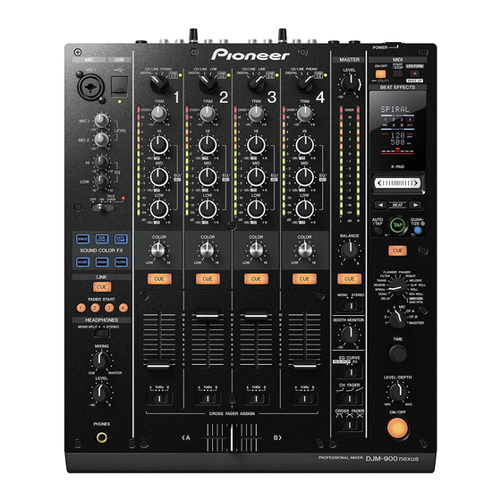
Page 10: Panel Facilities
2.2 PANEL FACILITIES DJM-900NXS... - Page 11 DJM-900NXS...
- Page 12 DJM-900NXS...
-
Page 13: Basic Items For Service
3.2 JIGS LIST Jigs List Jig Name Part No. Purpose of use / Remarks USB cable GGP1193 for PC connection, accessory Lubricants and Glues List Name Part No. Remarks Lubricating oil GYA1001 Refer to "9.4 CONTROL PANEL SECTION (1/2)". DJM-900NXS... -
Page 14: Pcb Locations
DWX3193 2..FAD3 ASSY DWX3200 2..SEND ASSY DWX3195 2..FAD4 ASSY DWX3201 2..TRM1 ASSY DWX3203 2..FADC ASSY DWX3202 2..TRM2 ASSY DWX3204 2..MIC1 ASSY DWX3207 2..HPJK ASSY DWX3208 2..TRM3 ASSY DWX3205 2..TRM4 ASSY DWX3206 1..PNLA ASSY DWX3196 > 1..POWER SUPPLY ASSY DWR1492 DJM-900NXS... - Page 15 DJM-900NXS...
-
Page 16: Block Diagram
1 GNDD_REFA_2 3 V+3R3_REFA_2 2 VR_CFD JA9201 2 VR_CFD 3 V+3R3_REFA_2 1 GNDD_REFA_2 DKN1622-A 4 HP_R 4 HP_R 3 GNDHP_O 3 GNDHP_O 2 GNDHP_O 2 GNDHP_O 1 HP_L 1 HP_L PF03PP-B07 CN9201 CN3401 PHONES KM200NA4L AKM1275-A-TBB L= 75mm PF04PP-S12 L=125mm DJM-900NXS... - Page 17 1 +12V STBY 1 +12V STBY 2 +12V Switched 2 +12V Switched 3 +12V Switched 3 +12V Switched 4 GNDD 4 GNDD 5 GNDD 5 GNDD 6 STBY Control 6 STBY Control 7 RESET 7 RESET DKP3901-A WHITE L=225mm DJM-900NXS...
-
Page 18: Audio System Block Diagram
4.2 AUDIO SYSTEM BLOCK DIAGRAM DJM-900NXS... - Page 19 DJM-900NXS...
-
Page 20: Dsp Block Diagram
4.3 DSP BLOCK DIAGRAM DJM-900NXS... - Page 21 DJM-900NXS...
-
Page 22: Power Block Diagram
PNLA ASSY GNDD_REFA FAD2 ASSY V+3R3D_REFA GNDD_REFA FAD3 ASSY V+3R3D_REFA GNDD_REFA FAD4 ASSY V+3R3D_REFA GNDD_REFA PNLB ASSY FADC ASSY V+3R3D V+2R5D IC1402 V+3R3D V+5VBUS V+5D UCOM GNDD V+5D_LED USBI ASSY V+1R2D GNDHP V+34D_1 Tr SW V+34D Q1409 HPJK ASSY DJM-900NXS... - Page 23 CIRCUIT IC1407 -15VA SUPPLY P1209 ASSY V+5D V+12D IC1405 V+9HP V+15A_HP V+5D_LED IC1201 HP CIRCUIT V-15A_HP V-9HP IC1202 V+12D GNDD V+1R2D IC1406 V+12D +12V Switched P1204 V+34D_1 V+12D Tr SW V+3R3E V+12E +12V STBY IC1401 Q1409 MAIN_CPU IC1404 V+12STB DJM-900NXS...
-
Page 24: Diagnosis
ETHER UCOM-DSP: Standby for response to handshake request DSP version setting ETHER UCOM-DSP: Handshake request and response ETHER UCOM-DSP: Standby for handshake response ETHER UCOM-DSP: Handshake response Canceling reset of SUBIC Canceling reset of PHY ETHER UCOM-MAIN CPU: Handshake request DJM-900NXS... - Page 25 Main program RAM transfer transfer Notifying of completion of normal DSP startup Updater start Initialization process of main microcomputer Program start Entering main loop Multitasking start Completion of ETHER UCOM initialization Notification of completion of ETHER UCOM initialization MUTE setting OFF DJM-900NXS...
-
Page 26: Troubleshooting
Check that all the cables are securely 4.1 OVERALL Securely connect the cables. If a cable is breakage, or connected. Relevant part CONNECTION broken, replace it. loose connection Check that there is no breakage in the DIAGRAM of internal cables cables. DJM-900NXS... - Page 27 If no signal is input, check for the signal supply [Communication line] MAIN ASSY 1-53 R2335 source of the CLK signal and repair it if it has an 1-54 Check that the signal level of SH_FPGA_ [Communication line] error. 10.41 WAVEFORMS DONE is High. MAIN ASSY 1-54 DJM-900NXS...
- Page 28 The unit is shut down in error by the Power Monitoring Circuit. Cause Diagnostics Point Item to be Checked Corrective Action Reference Check for power at each point, following 5.4 VOLTAGE MONI- See "5.4 VOLTAGE Power failure Repair the defective parts. TORING CIRCUIT “5.4 VOLTAGE MONITORING CIRCUIT.” MONITORING CIRCUIT.” DJM-900NXS...
- Page 29 Check if an audio signal is output from the improperly soldered or defective. INPUT ASSY /defective parts 2-16 IC5002(CH3 LINE) operation amplifier. • If an audio signal is output, go to [8]. IC5401(CH4 PHONO) IC5402(CH4 CD) 1 pin, 7 pin Representative CH1 LINE R 2-16 DJM-900NXS...
- Page 30 • If any of the signals is not output, IC110(CH1) Check for the LRCKO, BCKO, SCKO, /defective parts • BCKO: 11 pin DOUT signal output from DIR. /IC202(CH2)/IC302(CH3)/IC402(CH4) may be 1-7 1-10 • SCKO: 4 pin improperly soldered or defective. • DOUT: 12 pin Representative 1-7 1-10 DJM-900NXS...
- Page 31 Check for the RESET signal. IC4005 2 pin, 3 pin /defective parts INPUT ASSY • lf a signal at Pin 2 is H and that at Pin 3 is 2-7 2-12 2-7 2-12 normal, IC4005 must be improperly soldered or defective. DJM-900NXS...
- Page 32 [Checking the RESET signal path] 10.41 WAVEFORMS the parts mounted along the communication line. /defective parts Check for the RESET signal. R709 MAIN ASSY 1-28 1-28 • If no problem is found, ETHER UCOM (IC501) may be improperly soldered. DJM-900NXS...
- Page 33 Check that the MUTE_M1 (test land) signal 10.41 WAVEFORMS signal is not output properly, go to [13]. /defective parts MUTE_M1 1-102 level is Low. MAIN ASSY 1-102 • If it is L, RY2801/RY2802 must be improperly soldered or defective. DJM-900NXS...
- Page 34 Check the audio signals input to and output 1-127 1-128 /defective parts parts must be improperly soldered or defective. 1-127 1-128 from IC3203/IC3204. IC3204 • If no signal is input to IC3203/IC3204, go to [3]. 1-125 1-126 1-125 1-126 1-129 1-130 1-129 1-130 DJM-900NXS...
- Page 35 Check that the CPU_MUTE signal level is 10.41 WAVEFORMS CPU_MUTE 1-38 go to [13] of [3-1] No signal is output from the /defective parts MAIN ASSY High. 1-38 MASTER1/MASTER2 connectors. • If no problem is found, RY3401 must be improperly soldered or defective. DJM-900NXS...
- Page 36 If the DOUT_MS_SEL signal is not supplied properly, check for R711. If no problem is found, Ether UCOM (IC501) must be improperly soldered or defective. • If both are normal and no signal is output from IC2404, IC2404 must be improperly soldered or defective. DJM-900NXS...
- Page 37 • If the voltage at Pin 5 (V+5VBUS) of CN1802 is 1-37 V+5VBUS /defective parts CN1802 is about 5 V (4.75 to 5.25) using a PC not about 5 V (4.75 to 5.25), replace the USBI USBI Assy connected. Assy. DJM-900NXS...
-
Page 38: Indicator (Fl/Led) Not Lit
SUB UCOM (IC6601) port may be 80 pin 4-20 4-20 defective. Replace it. PNLA Assy Check for the voltage (2.7–4.2 V) at both If no voltage is detected, the LED may be Defective LED CN6601 electrodes of the LED. defective. Replace it. 11⇔12 pin DJM-900NXS... - Page 39 [Communication line] 1-19 [Communication line] • Check for the MII BUS line. Representative R1631 10.41 WAVEFORMS MAIN ASSY 1-19 If the symptom persists after the above ETHER-PHY (IC1603) may be defective. Part defective MAIN Assy — corrections. Replace it. DJM-900NXS...
-
Page 40: Information On Power Diagnostics
FL.,LED, V+12STB 11.3-12.7 LED(X-PAD,LFO FORM) V+3R3D 3.15-3.45 FL.,SUB UCOM(IC6601) V+34D 31-36 V+3R3D_REFA 3.15-3.45 CH1-4 FADER,CROSS FADER PNLB ASSY V+3R3D_REFA 3.15-3.45 CROSS FADER CDCB ASSY V+3R3 3.15-3.45 CDC SENSOR(IC3601) ex)V+5A_* • • • • • V+5A_BO,V+5A_HP,V+5A_M1 etc • • • DJM-900NXS... -
Page 41: Voltage Monitoring Circuit
R 1 2 2 2 To Power Block V+5A A side V A D E T Low value Hi value V+5A 4.28V 5.61V V-15A_1 V-15A_1 9.94V GNDD V+9HP 8.23V GNDD D1201 -11.82V V-9HP -5.96V 1SS301 16.74V V+15A 13.38V -18.57V V-15A -11.83V DJM-900NXS... - Page 42 V+3R3D < 2.85V > 3.81V V+2R5D < 2.22V > 2.81V V+1R2D < 1.08V < 1.08V When an > 1.32V > 1.32V error is V+15A < 13.38V generated > 16.74V V-15A < -18.57V > -11.83V V+5A < 4.28V > 5.61V DJM-900NXS...
-
Page 43: About The Protector
Diagnostic procedures when the wire for an ICP is broken 1. Unplug the AC power cord. 2. Check for any error, such as short-circuiting or defective parts, in the circuits subsequent to the ICP. 3. Repair the detective part. 4. Replace the ICP. DJM-900NXS... -
Page 44: Diagnosis Of V+34D
If the output signal from IC1403 is L, the mounting status of IC1403 may be improper or IC1403 itself may be defective. 5 If the output signal from IC1403 is H, the mounting status of the peripheral parts of Q1408 or Q1409 may be improper or Q1408/Q1409 may be defective. MAIN ASSY DJM-900NXS... -
Page 45: Error Indications
Please update it again. Download the update file again then ERROR E008 Update file error perform updating. ERROR EE00 LINK cutting error Please update it again. ERROR EEXX LINK error XX : Error generation task ID Please update it again. DJM-900NXS... -
Page 46: Connection Check With Each Interface
Devices to be added: • Universal Serial Bus controllers USB Composite Device • Under “Sound, video and game controllers” PIONEER DJM-900nexus USB Audio Device A communication check may be easily performed if connection is made with Device Manager displayed on the PC screen. -
Page 47: Service Mode
Mode 4 SOUND (Rear panel) COLOR POWER ON Test Mode LINK CH-1 Mode 5 Mode 11 (Mode 1) SPACE Mode 6 Mode 10 Mode 9 Mode 8 Mode 7 POWER SW Test Mode : CANCEL (Rear panel) POWER OFF DJM-900NXS... - Page 48 BEAT BEAT BEAT c button c button c button BEAT BEAT Software Name FL Display c button d button System MAIN CPU SUB UCOM DSP (program) DSP (data) ETHER UCOM USB UCOM FPGA BOOT DJM-900NXS...
- Page 49 LFO FORM (WAKE UP) button LED ON/OFF (UTILITY) button ON/OFF (UTILITY) button LED MD_ON START/STOP button None MD_ST BEAT c button None BEAT< BEAT d button None BEAT> AUTO/TAP button None AUTO QUANTIZE button QUANTIZE button LED GRID ON/OFF button ON/OFF button LED EFXon DJM-900NXS...
- Page 50 CH2 Channel Level Indicator LED selector switch : EQ -2dB : Left -1dB CH FADER : MID CH3 Channel Level Indicator LED selector switch : Right : Left -1dB CROSS FADER : MID CH4 Channel Level Indicator LED selector switch : Right DJM-900NXS...
- Page 51 This mode is also used to check operation of the TIME control. The value displayed on the FL display increases/decreases as you turn the TIME control: Minimum value Initial value Maximum value Operation range Initial value: 0 Maximum value: 100 Minimum value: -100 Turn Turn counterclockwise. clockwise. DJM-900NXS...
- Page 52 MIDI LFO FADER START SND/ RTN CF.A CF.B HEADPHONES BOOTH MONITOR MASTER MONO SPLIT STEREO TIME MIXING EQ CURVE ISOLATOR MASTER LEVEL / DEPTH LEVEL CH FADER THRU THRU THRU THRU CROSS FADER ON / OFF CROSS FADER ASSIGN PHONES DJM-900NXS...
- Page 53 EQ HI control Master Level Indicator L LED "+12": Full Illuminate "-12": Lights off EQ LOW control Master Level Indicator R LED "+12": Full Illuminate "LOW": Lights off CH1 COLOR control At the bottom of the FL display "HIGH": Full Illuminate DJM-900NXS...
- Page 54 MASTER LEVEL control Master Level Indicator L LED "0": Full Illuminate "L": Lights off BALANCE control Master Level Indicator R LED "R": Full Illuminate "LOW": Lights off CH3 COLOR control At the bottom of the FL display "HIGH": Full Illuminate DJM-900NXS...
- Page 55 DELAY MIDI LFO SND/ RTN CF.A CF.B HEADPHONES BOOTH MONITOR MASTER MONO SPLIT STEREO TIME MIXING EQ CURVE ISOLATOR MASTER LEVEL / DEPTH LEVEL CH FADER THRU THRU THRU THRU CROSS FADER ON / OFF CROSS FADER ASSIGN PHONES DJM-900NXS...
- Page 56 CH2 CUE button CH2 Channel Level Indicator LED CH3 CUE button CH3 Channel Level Indicator LED CH4 CUE button CH4 Channel Level Indicator LED MASTER CUE button Master Level Indicator L LED EFFECT CUE button Master Level Indicator R LED DJM-900NXS...
- Page 57 CH and X-PAD sections on the FL display X-PAD section: The 25th, 26th, and 27th segments light. CH section: Red frame around MST X-PAD Sensor 8 CH and X-PAD sections on the FL display X-PAD section: The 29th, 30th, and 31th segments light. DJM-900NXS...
- Page 58 If the CUE button is pressed while the last VR on each group list is displayed, the top VR on that group list will then be displayed. When the BEAT c, d button is pressed for a layer lower than the 2nd one, the top VR on the list of the next group will be displayed. DJM-900NXS...
- Page 59 "-∞": 000 LEVEL control HP_LV "0": 3FE *As an AD value that is displayed on the FL display is the one before a hysteresis removal process, and as it has an amplitude, an error of about ±2 may be produced. DJM-900NXS...
- Page 60 "MIN": 000 LEVEL/DEPTH control LV/DP "MAX": 3FE *As an AD value that is displayed on the FL display is the one before a hysteresis removal process, and as it has an amplitude, an error of about ±2 may be produced. DJM-900NXS...
- Page 61 FL Display Name Remarks "0": 000 CH1 Channel Fader "10": 3FE "0": 000 CH2 Channel Fader "10": 3FE "0": 000 CH3 Channel Fader "10": 3FE "0": 000 CH4 Channel Fader "10": 3FE "A": 000 Cross Fader CROSS "B": 3FE DJM-900NXS...
- Page 62 Properly operating: Address value, Not properly operating: EE *2 *1 “EE” is also displayed while the IP address is being obtained. If “EE” is displayed for more than 15 seconds, something is wrong. *2 “EE” is also displayed before the subnet mask data are obtained. DJM-900NXS...
- Page 63 CH3 COLOR CH1 CUE CH2 CUE CH3 CUE CH4 CUE BOOTH EQ HI MIXING MASTER LEVEL MONITOR CH1 CUE CH3 CUE CH2 CUE CH4 CUE EQ LOW BALANCE LEVEL LEVEL/ DEPTH CH3 CUE CH1 CUE CH2 CUE CH4 CUE DJM-900NXS...
-
Page 64: About The Device
IC6601 PNLA Assy CDC SENSOR Contact position detection of a X-PAD AD7147ACPZ500RL7 IC3601 CDCB Assy Two or more FLASH and SDRAM are mounted in this unit. Please judge the device which you should diagnose in reference to this list. DJM-900NXS... -
Page 65: Disassembly
White Slider Knob 2 Black Black Black White White Slider Knob 1 Rotary Knob Low (BN) Select Knob Rotary SW Knob (C) (DAA1265) ×1 (DAA1205) ×1 (DAA1180) ×1 Black White White Slider Knob Stopper Black Black Gray Black Projection DJM-900NXS... - Page 66 (3) Remove the four rotary SW knob S (C). Rotary SW knob S (C) ×2 (4) Remove the two screws. (BBZ30P060FTB) (5) Remove the two screws. (BBZ30P060FTC) Washer ×2 (6) Remove the two screws. (BPZ30P120FTB) (7) Remove the six screws. (CCZ30P080FTB) ×3 Screw tightening order ×3 ×2 DJM-900NXS...
- Page 67 (1) Disconnect the four short pin plugs. ×2 ×2 (2) Remove the three washers and three nuts. (3) Remove the two screws. (PMH30P100FTB) (4) Remove the one screw. (BBZ30P060FTB) ×2 (5) Remove the four screws. (BPZ30P080FTB) ×2 • Rear view Nut tightening order DJM-900NXS...
- Page 68 TRIM Bracket Screw tightening order Center Stay (7) Lift up the INPUT Assy to a front direction. Control panel section PNLA Assy PNLB Assy INPUT Assy Diagnosis ACSW Assy FADC Assy HPJK Assy MAIN Assy SEND Assy POWER SUPPLY Assy DJM-900NXS...
- Page 69 Bracket PSW ACSW Assy Screw tightening order (MAIN, SEND Assy) Screw tightening order (AC shield) MAIN Assy SEND Assy AC shield Nut tightening order (INPUT Assy) Screw tightening order (USB bracket) USB panel TRIM bracket INPUT Assy USB bracket DJM-900NXS...
- Page 70 Slider knob 2 *: During reassembly, fully push down Slider knob 2 until it is Tweezers Protective material dented into Slider knob 1. 4 Remove the slider knob 1. 5 Remove the slider knob stopper. Slider knob 1 Slider knob stopper DJM-900NXS...
- Page 71 (2) Disconnect the one flexible cable. (CN5601) (3) Remove the one screw. (BPZ26P080FTC) (4) Remove the CDC holder. CDC holder (5) Disconnect the one flexible cable. (CN3601) (6) Remove the CDCB Assy. CN5601 CDCB Assy CN3601 CDC panel • Bottom view DJM-900NXS...
- Page 72 • Connectors color Match the color of a connected connector. ×4 CN7002 ×2 FAD1 FAD4 (White) (Yellow) FAD2 FAD3 (Red) (Blue) FADC Assy Screw tightening order FAD1 FAD2 FAD3 FAD4 FADC Assy Assy Assy Assy Assy CRF stay FADC Assy DJM-900NXS...
- Page 73 Shaft holder Note: FAD Assy The grease application position when you assemble guide shaft(S) refer to "9.4 CONTROL PANEL SECTION (1/2)." [3-4] PNLA and PNLB Assy (1) Remove the 30 flange nuts M9. ×30 (2) Remove the one nut. DJM-900NXS...
- Page 74 (12) Remove the 12 screws. (BBZ30P060FTC) (13) Remove the barrier. (14) Remove the 10 screws. (BBZ30P060FTC) ×12 (15) Remove the PNLA and PNLB assemblies. Barrier Screw tightening order ×10 PNLA Assy PNLA Assy PNLB Assy • Bottom view PNLB Assy DJM-900NXS...
-
Page 75: Each Setting And Adjustment
VFD. (No need to update it if current version shows as x.xx. It is the latest firmware.) <STEP3> Connect your computer with this unit by LAN cable. Connect LAN cable to the LINK terminal on rear on this unit. DJM-900NXS... - Page 76 (For Windows XP, check the checkbox “Notify me when this <STEP 2> connection has limited or no connectivity.”) Open "Network and Sharing Center." (For Windows XP, go to <STEP 4>. <STEP 3> Open "Change adapter setting". <STEP 6> Select "Obtain an IP address automatically","Obtain DNS server address automatically". DJM-900NXS...
- Page 77 Select "Notification area" then "Customize." (For Windows Vista, check the “Network” checkbox.) <STEP 10> Select "Show icon and notifications" on network. <STEP 11> Close "Properties" by "OK". For Mac OS X Select “System Environment Settings,” “Network,” “Ethernet,” then “Using DHCP” DJM-900NXS...
- Page 78 Check the cable is connected. Checking the status of connection. Wait a minute. is connected. DJM-900NXS Start update tool. For Mac OS X Check the connection status of the PC and this unit, by selecting “System Environment Settings,” “Network,” then “Ethernet.”...
- Page 79 U P D AT E Ve r X . X X <STEP1> Press [CUE (BEAT EFFECT)] and [ON/OFF (BEAT EFFECT)] with power button. Move to update mode. <STEP2> Check it is the latest version. Update was completed if it shows "x.xx". DJM-900NXS...
- Page 80 Failed data transfer to mixer. The file might have a problem. Data Transfer Error Cannot find the UpdateFile_S2 Stand up mixer again by update mode and restart the application. Failed data transfer to mixer. Cannot find the UpdateFile_S3 Stand up mixer again by update mode and restart the application. DJM-900NXS...
-
Page 81: How To Confirm The Dvs
(indicated with a red frame) is set to the minimum volume position. If the MAIN volume indicators are not displayed on the screen, set the TRAKTOR screen to Full screen. [Connection Diagram (When the CDJ Player is Connected to CH1)] DJM-900nexus DJM-900nexus Computers USB cable Power amplifier CDJ player DJM-900NXS... - Page 82 Settings for the Driver Start up the "DJM-900nexus Settings Utility". (Reference) For Windows Click [Start] menu → [All Programs] → [Pioneer] → [DJM-900nexus] → [DJM-900nexus Settings Utility]. MIXER INPUT MIXER OUTPUT When the DIGITAL, CD/LINE, PHONO, LINE, and Set the Timecode CD/LINE.
- Page 83 2 Click on the b symbol beneath A to D then select “Audio Through” from the pulldown menu. 3 Select Traktor then Preferences, or click on the Preferences button. Preferences button DJM-900NXS...
- Page 84 Output Channel A-D, as shown in the figure below. “Tpro Ext.Mixer - 4Deck.” 6 In Input Routing, set Input Channel A–D, as shown in the After confirming that 4Deck is added to Layout, close the figure below. Preferences window, by clicking on the Close (×) button. DJM-900NXS...
-
Page 85: User Setable Items
MAIN UTILITY Digital Out Sampling Rate DOUT FS 48kHz/96kHz 96kHz setting MASTER ATT. MST ATT -6dB/-3dB/0dB CLUB Auto Standby AUTOSTB ON/OFF SETUP Mic Output To Booth Monitor MIC BTH ON/OFF PC Utility PC UTLY ON/OFF Factory Reset INITIAL YES/NO DJM-900NXS... -
Page 86: Sheet For Confirmation Of The User Setting
Digital Master Out Level -19dB -15dB -10dB -5dB Digital Out Sampling Rate 48kHz 96kHz MASTER ATT. -6dB -3dB Auto Standby Mic Output To Booth Monitor PC Utility Factory Reset NEVER perform FACTORY RESET before taking note of setting data. DJM-900NXS... - Page 87 DJM-900NXS...
-
Page 88: Exploded Views And Parts List
Screws adjacent to b mark on product are used for disassembly. For the applying amount of lubricants or glue, follow the instructions in this manual. (In the case of no amount instructions, apply as you think it appropriate.) 9.1 PACKING SECTION SYXJ8 only KXJ5 only DJM-900NXS... - Page 89 14 Pad B DHA1855 15 Packing Case See Contrast table (2) 16 Packing Sheet RHC1023 (2) CONTRAST TABLE DJM-900NXS/SYXJ8, UXJCB, LXJ, KXJ5 and XJCN5 are constructed the same except for the following: DJM-900NXS DJM-900NXS DJM-900NXS DJM-900NXS DJM-900NXS Mark Symbol and Description...
-
Page 90: Exterior Secion
9.2 EXTERIOR SECION Refer to "9.4 CONTROL PANEL SECTION (1/2)" . UXJCB only UXJCB only UXJCB, LXJ, KXJ5 only UXJCB only UXJCB only Refer to "9.3 BOTTOM SECTION" . DJM-900NXS... - Page 91 PMH30P100FTB 23 Front Panel DNK5845 24 USB Panel DNK5847 25 USB Cover B DNK5868 (2) CONTRAST TABLE DJM-900NXS/SYXJ8, UXJCB, LXJ, KXJ5 and XJCN5 are constructed the same except for the following: DJM-900NXS DJM-900NXS DJM-900NXS DJM-900NXS DJM-900NXS Mark Symbol and Description...
-
Page 92: Bottom Section
9.3 BOTTOM SECTION PNLA CN6602 HPJK CN9201 INPUT USBI CN4002 CN3801 INPUT CN4003 UXJCB only *Note: During MAIN Assy disassembly, if the silicone sheet is found to be deformed, replace it with a new one. DJM-900NXS... - Page 93 IBZ30P080FTB 32 Screw IMZ30P040FTC 33 Screw PPZ30P080FTB 34 Screw See Contrast table (2) (2) CONTRAST TABLE DJM-900NXS/SYXJ8, UXJCB, LXJ, KXJ5 and XJCN5 are constructed the same except for the following: DJM-900NXS DJM-900NXS DJM-900NXS DJM-900NXS DJM-900NXS Mark Symbol and Description /SYXJ8...
-
Page 94: Control Panel Section (1/2)
After applying grease, move the slider base back and forth from one end to the other for approximately 10 to 20 strokes, in order to fully spread the grease. Refer to Nut: Attached part of "9.5 CONTROL PANEL SECTION (2/2)" . Rotary encoder (DSX1068) DJM-900NXS... - Page 95 36 Button (CUE) DAC2503 37 Slider Knob 1 DAC2684 38 Slider Knob 2 DAC2685 39 FL Panel DAH2829 40 Fader Panel DAH2830 41 CDC Sheet DEC3325 42 Control Panel DNB1186 43 Lens DNK4532 44 CDC Panel DNK5846 45 Lens (USB) DNK5848 DJM-900NXS...
-
Page 96: Control Panel Section (2/2)
9.5 CONTROL PANEL SECTION (2/2) • Bottom view MAIN CN1001 DJM-900NXS... - Page 97 12 Button (LINK) DAC2654 13 Button (MIDI) DAC2655 14 Button (CFX) DAC2656 15 Lens Holder DNK4533 16 Lens Holder (S) DNK5849 17 Lebel Meter Assy DXB1882 18 • • • • • 19 • • • • • 20 Screw BBZ30P060FTC DJM-900NXS...
-
Page 98: Schematic Diagram
R 4 0 0 6 GNDD GNDD R 4 0 1 1 R 4 0 0 7 R 4 0 1 2 R 4 0 0 8 GND_PO GND_PO GNDA_1 GNDA_2 1/21 CN1002 GNDA_2T GNDA_1T GNDA_3 GNDA_3T 1/11 GNDF DJM-900NXS... - Page 99 R 4 0 6 4 To CH1 INPUT Block CH2 INPUT Block GNDD R 4 0 5 2 CH3 INPUT Block CH4 INPUT Block GNDD GNDF (GNDA) GNDA_4 G N D D _ R E F A GNDA_4T 2/21 CN1203 GNDF 1/11 DJM-900NXS...
-
Page 100: Input Assy (2/11)
Q 4 2 0 6 0 . 1 u / 2 5 GNDF V-15A_IN V-15A_IN GND_PO R 4 2 0 2 1 0 0 LINE 1/11 GNDF From BOARD IF L I N E _ S E L 1 2/11 1:2F DJM-900NXS... - Page 101 RS1/16SS***J (L1) : CH1 LINE Signal (L CH) RS1/10SE****D (CH1 A) RN1/16SE****D : CH1 Audio Signal (L CH) CKSRYB (CH1 T) CKSSYB : CH1 Timecode Signal (L CH) CKSYB CFHXSQ CCSRCH CCSSCH CFTLA CEJQ CEANP CEAT CEHAT CEHAZL 2/11 DJM-900NXS...
-
Page 102: Input Assy (3/11)
L R C L K _ I N _ C H 1 1:11D B C L K _ I N _ C H 1 1/11 1:11C M C L K _ I N _ C H 1 1:11B T C _ S E L 1 3/11 1:2F DJM-900NXS... - Page 103 R 4 4 7 6 R 4 4 7 0 select H C S 5 3 8 1 - K Z GND_PO V-15A_IN 1 0 k (TIMECODE) CH1_ADAT (CH1 D) GNDD CH1_ADAT Time R 4 4 7 4 (CH1 D) 2-27 GNDA_1T 3/11 DJM-900NXS...
-
Page 104: Input Assy (4/11)
H N 1 C 0 1 F U ( Y G R ) 0 . 1 u / 2 5 GNDF V-15A_IN GND_PO V-15A_IN R 4 6 1 1 1 0 0 LINE GNDF 1/11 4/11 From BOARD IF L I N E _ S E L 2 1:2E DJM-900NXS... - Page 105 : CH2 LINE Signal (L CH) (CH2 A) NOTES is STBY : CH2 Audio Signal (L CH) (CH2 T) RS1/10SR***J : CH2 Timecode Signal (L CH) RS1/16SS***J RS1/10SE****D RN1/16SE****D CKSRYB CKSSYB CKSYB CFHXSQ CCSRCH CCSSCH CFTLA CEJQ CEANP CEAT CEHAT CEHAZL 4/11 DJM-900NXS...
-
Page 106: Input Assy (5/11)
L R C L K _ I N _ C H 2 1:11D B C L K _ I N _ C H 2 1:11C 1/11 M C L K _ I N _ C H 2 1:11B T C _ S E L 2 1:2F 5/11 DJM-900NXS... - Page 107 R 4 8 7 6 R 4 8 7 0 select H C S 5 3 8 1 - K Z GND_PO V-15A_IN (TIMECODE) 1 0 k CH2_ADAT GNDD (CH2 D) R 4 8 7 4 CH2_ADAT Time (CH2 D) NDA_2T 5/11 DJM-900NXS...
-
Page 108: Input Assy (6/11)
Q 5 0 0 8 0 . 1 u / 2 5 GNDF V-15A_IN GND_PO V-15A_IN R 5 0 1 1 1 0 0 LINE GNDF 1/11 6/11 From BOARD IF L I N E _ S E L 3 1:7E DJM-900NXS... - Page 109 : CH3 LINE Signal (L CH) RS1/10SR***J (CH3 A) : CH3 Audio Signal (L CH) RS1/16SS***J (CH3 T) RS1/10SE****D : CH3 Timecode Signal (L CH) RN1/16SE****D CKSRYB CKSSYB CKSYB CFHXSQ CCSRCH CCSSCH CFTLA CEJQ CEANP CEAT CEHAT CEHAZL 6/11 DJM-900NXS...
-
Page 110: Input Assy (7/11)
L R C L K _ I N _ C H 3 1:10D B C L K _ I N _ C H 3 1/11 1:10C M C L K _ I N _ C H 3 1:10B T C _ S E L 3 1:7E 7/11 DJM-900NXS... - Page 111 R 5 2 7 6 (AUDIO) R 5 2 7 0 C S 5 3 8 1 - K Z GND_PO V-15A_IN select H 1 0 k CH3_ADAT GNDD (TIMECODE) R 5 2 7 4 (CH3 D) CH3_ADAT Time (CH3 D) NDA_3T 7/11 DJM-900NXS...
-
Page 112: Input Assy (8/11)
Q 5 4 0 6 0 . 1 u / 2 5 GNDF V-15A_IN V-15A_IN GND_PO R 5 4 0 2 1 0 0 LINE GNDF 1/11 L I N E _ S E L 4 From BOARD IF 8/11 1:7F DJM-900NXS... - Page 113 : CH4 LINE Signal (L CH) RS1/10SR***J (CH4 A) : CH4 Audio Signal (L CH) RS1/16SS***J RS1/10SE****D (CH4 T) : CH4 Timecode Signal (L CH) RN1/16SE****D CKSRYB CKSSYB CKSYB CFHXSQ CCSRCH CCSSCH CFTLA CEJQ CEANP CEAT CEHAT CEHAZL 8/11 DJM-900NXS...
-
Page 114: Input Assy (9/11)
L R C L K _ I N _ C H 4 1:10D B C L K _ I N _ C H 4 1/11 1:10C M C L K _ I N _ C H 4 1:10B T C _ S E L 4 9/11 1:7F DJM-900NXS... - Page 115 R 5 6 7 6 R 5 6 7 0 (AUDIO) C S 5 3 8 1 - K Z GND_PO V-15A_IN 1 0 k select H CH4_ADAT GNDD (TIMECODE) (CH4 D) R 5 6 7 4 CH4_ADAT Time (CH4 D) GNDA_4T 9/11 DJM-900NXS...
-
Page 116: Input Assy (10/11)
R 5 8 0 5 R 5 8 0 7 DKN1614-A (2/2) 1 0 u / 5 0 1 0 0 3 6 k RNB4580F V-15A_IN C 5 8 0 6 GNDF GNDF Pull up & ESD Main side 10/11 DJM-900NXS... - Page 117 R E T U R N _ I N : Waveform measuring point NOTES is STBY (RET A) RS1/10SR***J : RETURN Audio Signal (L CH) RS1/16SS***J (RET D) : RETURN DIGITAL Signal RS1/10SE****D RN1/16SE****D CKSRYB CKSSYB CKSYB CFHXSQ CCSRCH CCSSCH CFTLA CEJQ CEANP CEAT CEHAT CEHAZL 10/11 DJM-900NXS...
-
Page 118: Input Assy (11/11)
G N D 2 2 0 GNDD TC7S04FU V+5D_IN V+5D_IN Q 6 2 0 1 L T C 1 2 4 E U B GNDD GNDD 1SS302 1SS302 D6201 D6202 GNDD GNDD DNH2736-A / SHIELD CASE(MIDI) GNDD GNDD 11/11 DJM-900NXS... - Page 119 A D A T _ M I C _ A N A D G N D S D T O GNDF GNDF GNDF 1:2F (MIC D) 2-47 AK5358AET C2 TRIM 2-48 ADAT_MIC_ANA 2-46 1/11 GNDF 1/11 M I D I _ T X D 1:2F 11/11 DJM-900NXS...
-
Page 120: Mic1 And Trm1 To Trm4 Assys
V R 8 4 0 1 D C S 1 1 1 9 - A D C S 1 1 1 9 - A C 8 2 0 1 C 8 4 0 1 0.1u 0.1u 2/11 4/11 CN4201 CN4601 B C D DJM-900NXS... - Page 121 V R 8 8 0 1 D C S 1 1 1 9 - A D C S 1 1 1 9 - A C 8 6 0 1 C 8 8 0 1 0.1u 0.1u 6/11 8/11 CN5001 CN5401 DJM-900NXS...
-
Page 122: Main Assy (1/21)
9 6 K _ C L K _ A I N 13/21 13:3J 6 M _ C L K _ A I N From FPGA Block 13:3J 2 4 M _ C L K _ A I N 1/21 DJM-900NXS... - Page 123 15/21 15:13G (RET D) ADAT_RETURN_ANA (CH4 D) 15:13G ADAT_CH4_ANA 15:13G (CH3 D) ADAT_CH3_ANA R 1 0 2 9 12:14D M I D I _ T X D BOARD IF 12:14C VR_TRIM3 12/21 12:14C VR_TRIM4 12:14C VR_TRIM1 12:14C VR_TRIM2 1/21 DJM-900NXS...
-
Page 124: Main Assy (2/21)
K N 1 2 0 5 K N 1 2 0 6 GNDD C K F 1 0 8 9 - A C K F 1 0 8 9 - A C K F 1 0 8 9 - A 2/21 DJM-900NXS... - Page 125 RS1/8S****J 1/4W RS1/4S****J RS2****J C N 1 2 0 4 V+12D RAB4CQ****J GNDD CKSRYB**** CKSSYB**** STBY CCSRCH**** ECIAL MODEL LED CCSSCH**** WER SUPPLY STB CCSQCH**** CEVW*** CEHVAW** 12/21 CEVWNP*** 12:2E P-CON From To Main Ucom 3:2F;12:2H PowerReset 3/21,12/21 2/21 DJM-900NXS...
-
Page 126: Main Assy (3/21)
F L _ V c o n t 12/21 High The > mark found on some component parts indicates the importance of the safety factor of the part. Therefore, when replacing, be sure to use parts of identical designation. 3/21 DJM-900NXS... - Page 127 0 . 1 u / 1 6 STBY C O M P GNDD G N D BD9325FJ 2A parts V+34D TPUT STBY G N D D G N D D _ L E D : Voltage measuring point : Waveform measuring point 3/21 DJM-900NXS...
-
Page 128: Main Assy (4/21)
D S S 1 2 0 2 - A CKSRYB**** 22.5792MHz CKSSYB**** 5pin Y 24.576MHz 22.5792MHz CCSRCH**** CCSSCH**** G N D D G N D D CCSQCH**** fs=96kHz 256fs CEVW*** 22.5792MHz 24.576M fs=48kHz 512fs CEHVAW** 4/21 CEVWNP*** 22.5792M fs=44.1kHz 512fs DJM-900NXS... - Page 129 G N D D XTI = 22.5792MHz 11:2H 44.1KHz G N D USBOUT_SRC_MS_SEL 9 6 K _ C L K _ U S B 11/21 I C 1 1 8 G N D D TC7SH08FUS1 DIGITAL IN_1 : Waveform measuring point 4/21 DJM-900NXS...
-
Page 130: F 10.17 Main Assy (5/21)
R 2 1 2 4:15I;6:3J;7:3J 6 M _ C L K _ U S B O U T From DIGITAL_IN1 R 2 1 3 4:15I;6:3J;7:3J 9 6 K _ C L K _ U S B O U T 5/21 DJM-900NXS... - Page 131 1 0 0 V + 3 R 3 D MCLK_OUT TDM_IN (CH2 U/D OUT) TC74LCX157FK G N D D R 2 4 8 CS8421-CZ G N D D 4 7 k G N D D G N D D 5/21 DJM-900NXS...
-
Page 132: Main Assy (6/21)
R 3 1 2 4:15I;5:3J;7:3J 6 M _ C L K _ U S B O U T From DIGITAL_IN1 R 3 1 3 4:15I;5:3J;7:3J 9 6 K _ C L K _ U S B O U T 6/21 DJM-900NXS... - Page 133 1 0 0 MCLK_OUT TDM_IN V + 3 R 3 D (CH3 U/D OUT) TC74LCX157FK G N D D R 3 4 8 CS8421-CZ G N D D 4 7 k G N D D G N D D 6/21 DJM-900NXS...
-
Page 134: Main Assy (7/21)
R 4 1 2 4:15I;5:3J;6:3J 6 M _ C L K _ U S B O U T R 4 1 3 From DIGITAL_IN1 4:15I;5:3J;6:3J 9 6 K _ C L K _ U S B O U T 7/21 DJM-900NXS... - Page 135 1 0 0 MCLK_OUT TDM_IN V + 3 R 3 D (CH4 U/D OUT) TC74LCX157FK G N D D R 4 4 8 CS8421-CZ G N D D 4 7 k G N D D G N D D 7/21 DJM-900NXS...
-
Page 136: Main Assy (8/21)
G N D 2 G N D 1 D S S 1 2 0 5 - A 25MHz G N D D G N D D From LAN UCOM 9:15G R E S E T _ P H Y 9/21 8/21 DJM-900NXS... - Page 137 R 1 6 2 6 NOTES is STBY RS1/16S****J RS1/10S****J (LINK IN) RN1/16S****J : LINK AUDIO INPUT RN1/10S****J RS1/16S****D RS1/10S****D RS1/16S****F RS1/10S****F : Waveform measuring point 1/8W RS1/8S****J 1/4W RS1/4S****J RS2****J RAB4CQ****J CKSRYB**** CKSSYB**** CCSRCH**** CCSSCH**** CCSQCH**** CEVW*** CEHVAW** CEVWNP*** 8/21 DJM-900NXS...
-
Page 138: Main Assy (9/21)
V s s Q 1 3 Y 2 0 P L L V s s V s s Q 1 4 V s s Q 1 5 G N D D W 1 1 9/21 V s s Q 1 6 GNDD DJM-900NXS... - Page 139 R E S E T _ P H Y To LAN INPUT 8:3I NOTES is STBY RS1/16S****J RS1/10S****J RN1/16S****J RN1/10S****J RS1/16S****D RS1/10S****D RS1/16S****F RS1/10S****F : Waveform measuring point 1/8W RS1/8S****J 1/4W RS1/4S****J RS2****J RAB4CQ****J CKSRYB**** CKSSYB**** CCSRCH**** CCSSCH**** CCSQCH**** CEVW*** CEHVAW** CEVWNP*** 9/21 DJM-900NXS...
-
Page 140: Main Assy (10/21)
13:4F 6 M _ C L K _ L A N 13/21 13:4F From FPGA 2 4 M _ C L K _ L A N 13:4E 9 6 K _ C L K _ L A N 10/21 DJM-900NXS... - Page 141 G N D D 1-29 1-30 NOTES is STBY RS1/16S****J RS1/10S****J RN1/16S****J RN1/10S****J RS1/16S****D RS1/10S****D RS1/16S****F RS1/10S****F 1/8W RS1/8S****J 1/4W RS1/4S****J RS2****J RAB4CQ****J CKSRYB**** (LINK IN) CKSSYB**** : LINK AUDIO INPUT CCSRCH**** CCSSCH**** CCSQCH**** CEVW*** CEHVAW** : Waveform measuring point CEVWNP*** 10/21 DJM-900NXS...
-
Page 142: Main Assy (11/21)
From Main_Ucom U S B _ R E Q G N D D 12:14F U S B _ R C V 1-36 10:2G From LAN_Ucom U S B _ R E S E T 10/21 G N D D 11/21 DJM-900NXS... - Page 143 JTAG GNDD BF_TCK USB_RSET,USB_VREF use test mode BF_TRST not use then BF_TDI USB_RSET opne G N D D BF_TDO USB_VREF 0.1uF(GND) GNDD GNDD G N D D : Voltage measuring point U S B : Waveform measuring point 11/21 DJM-900NXS...
-
Page 144: Main Assy (12/21)
V C C R 2 0 1 3 R 2 0 1 8 G N D D G N D D G N D D G N D 12/21 24.576MHz(DSP/FPGA) I C 2 0 0 9 G N D D TC7SH08FUS1 DJM-900NXS... - Page 145 1 3 : 1 5 B To FPGA 2 4 M _ C L K _ F P G A 4/21 4 : 3 I To DIGITAL_IN1 2 4 M _ C L K _ U S B 12/21 DJM-900NXS...
-
Page 146: Main Assy (13/21)
DIGITAL_IN3 4:15B;5:15B;6:15B;7:15B DIGITAL_IN4 I N B V C C From CH4_SPDIF I N A DIGITAL_IN4 7:15B R 2 2 0 3 4/21-7/21 G N D O U T Y 13/21 G N D D R 2 2 0 2 DJM-900NXS... - Page 147 S H _ F P G A _ S C K 2 S H _ F P G A _ R S T _ X 1 0 : 1 5 G S H _ F P G A _ X I N I T 10:15I : Waveform measuring point 13/21 DJM-900NXS...
-
Page 148: Main Assy (14/21)
C V D D 1 9 C V D D 2 0 3216size L 7 0 4 G N D D R S V 1 C T F 1 5 7 9 - A 14/21 BLM31PG601SN1 R S V 2 G N D D DJM-900NXS... - Page 149 F L A S H _ D S P _ R E S E T From LAN_UCOM_2 10:2G NOTES is STBY RS1/16S****J RS1/10S****J RN1/16S****J RN1/10S****J RS1/16S****D RS1/10S****D RS1/16S****F RS1/10S****F 1/8W RS1/8S****J 1/4W RS1/4S****J RS2****J RAB4CQ****J CKSRYB**** CKSSYB**** _ D S P CCSRCH**** CCSSCH**** CCSQCH**** CEVW*** CEHVAW** : Waveform measuring point CEVWNP*** 14/21 DJM-900NXS...
-
Page 150: Main Assy (15/21)
U S B 0 _ V D D A 1 8 STBY (CH3 U OUT) U S B 0 _ V D D A 1 2 : CH3 USB Output Signal (CH4 U OUT) : CH4 USB Output Signal G N D D 15/21 DJM-900NXS... - Page 151 U S B 0 _ D R V V B U S / G P 4 [ 1 5 ] U S B 0 _ D P USB2.0 U S B 0 _ D M U S B 0 _ I D : Waveform measuring point 15/21 DJM-900NXS...
-
Page 152: Main Assy (16/21)
R 2 4 0 2 4:3G;13:4D R 2 4 0 6 G N D D 6 M _ C L K _ S R C G N D I C 2 4 0 2 G N D D TC7SH08FUS1 1-62 16/21 DJM-900NXS... - Page 153 G N D D XTAL:24.576MHz NOTES is STBY (DIG OUT) : DIGITAL OUT Signal RS1/16S****J RS1/10S****J RN1/16S****J : Waveform measuring point RN1/10S****J RS1/16S****D RS1/10S****D RS1/16S****F RS1/10S****F 1/8W RS1/8S****J 1/4W RS1/4S****J RS2****J RAB4CQ****J CKSRYB**** CKSSYB**** CCSRCH**** CCSSCH**** CCSQCH**** CEVW*** CEHVAW** CEVWNP*** 16/21 DJM-900NXS...
-
Page 154: Main Assy (17/21)
R 2 6 2 0 A D A T _ M A S T E R 15:3G 1/21 R 2 6 2 1 M V R _ M U T E 1:4B From BOARD IF Block (PANL A ) 17/21 DJM-900NXS... - Page 155 A D A T _ R E C _ O U T 18:2D 19/21 A D A T _ M A S T E R _ O U T To MASTER1 Block 18:2D M V R _ M U T E _ O U T 18/21 17/21 DJM-900NXS...
-
Page 156: Main Assy (18/21)
R 2 8 4 8 R 2 8 6 5 C 2 8 5 1 1 . 5 k 1 . 3 k 1 . 1 k 1 8 0 p / 5 0 17/21 CPU_MUTE_OUT From OUTPUT IF Block 17:9C 18/21 DJM-900NXS... - Page 157 L T C 1 2 4 E U B 19:2B M A S T E R 2 _ L - 18/21 19:2C V-15A_M1 M A S T E R 2 _ R + To MASTER2/REC Block 19:2D M A S T E R 2 _ R - DJM-900NXS...
-
Page 158: Main Assy (19/21)
1 0 u / 5 0 5 . 1 k 4 . 7 k 4 . 3 k R 3 0 3 2 V-15A_REC GNDA_REC 1/21,17/21,20/21 GNDA_ M U T E _ O U T 1:11C;17:9B;2D;20:2H MUTE release High MUTE Output AMP 19/21 DJM-900NXS... - Page 159 1 8 k CKSRYB**** GNDA_REC CKSSYB**** CCSRCH**** GNDA_REC CCSSCH**** GNDA_REC CCSQCH**** GNDA_REC CEVW*** CEHVAW** CEVWNP*** : Waveform measuring point (MA2 O) : MASTER2 OUT L ch (REC D) : REC OUT Digital Signal (REC O) : REC OUT L ch 19/21 DJM-900NXS...
-
Page 160: Main Assy (20/21)
R 3 2 9 0 R 3 2 9 1 5 . 6 k 4 . 7 k 3 . 9 k GNDA_BO GNDA_BO GNDA_BO 1/21,17/21,19/21 M U T E _ O U T 1:11C;17:9B;19:2D;19:2H MUTE release High MUTE 20/21 DJM-900NXS... - Page 161 R 3 2 4 5 CKSRYB**** CKSSYB**** R 3 2 4 3 CCSRCH**** CCSSCH**** 1 8 k CCSQCH**** Q 3 2 1 2 I N C 2 0 0 2 A C 1 CEVW*** GNDA_BO CEHVAW** CEVWNP*** MUTE release High MUTE 20/21 DJM-900NXS...
-
Page 162: Main Assy (21/21)
R 3 4 1 9 R 3 4 2 7 3 . 9 k 3 . 3 k 0 . 1 GNDA_HP GNDA_HP GNDA_HP 12/21,17/21 C P U _ M U T E From MAIN CPU Block 12:2F;17:2C 21/21 DJM-900NXS... - Page 163 L S A 1 5 7 6 U B ( Q R S ) Q 3 4 1 0 L T C 1 2 4 E U B R 3 4 4 8 MUTE High MUTE release GNDD_HP 21/21 DJM-900NXS...
-
Page 164: Usbi And Hpjk Assys
L 3 8 0 1 GNDD R T 2 GNDD STBY STBY STBY GNDD FGND FGND FGND FGND GNDD NOTES : Waveform measuring point is STBY RS1/16S****J (USB IN/OUT) RS1/10S****J : USB IN/OUT Signal CKSRYB**** CKSSYB**** CCSRCH**** CCSSCH**** CCSQCH**** DJM-900NXS... - Page 165 C N 9 2 0 1 KM200NA4L JA9201 R 9 2 0 5 DKN1622-A HP_L GNDHP_O R 9 2 0 4 GNDHP_O HP_R STBY STBY GNDF GNDHP_O1 R 9 2 0 3 GNDF GNDHP_O GND_F PHONE SHIELD:DNF1875- NOTES is STBY CKSRYB CFTLA RS1/10SR***J DJM-900NXS...
-
Page 166: Send Assy
R 6 4 0 1 RD1/2VM*** R 6 4 0 2 (SEND O) RS1/10SS****D (SEND D) RS1/10SR***J RS1/16SS***J R 6 4 0 3 CKSRYB R 6 4 0 4 CKSSYB CCSRCH CCSSCH GNDA_F GNDD_O GNDA_SE CCSQCH CEANP CEAT CEHAT CEHAZL DJM-900NXS... - Page 167 Q 6 4 0 4 I N C 2 0 0 2 A C 1 GNDA_SE : Voltage measuring point : Waveform measuring point (SEND O) : SEND Output Audio Signal (L CH) (SEND D) : SEND DIGITAL Signal DJM-900NXS...
-
Page 168: Pnla Assy (1/2)
HP_LEVEL D S G 2:7H L E V E L / D E P T H LEVEL/DEPTH V+3R3D_REFB_PA STBY GNDD_REFB V+3R3_REFB S 6 6 CFX6_SW CN7201 CN7401 CN7601 CN7801 GNDD D S G GNDD STBY GNDD GNDD_REFB_PA CN6603 52492-3120 DJM-900NXS... - Page 169 S 6 6 1 0 CFX6_SW CN7801 is STBY CFX6 D S G 1 0 7 9 - A C 6 6 5 5 RS1/10SR***J GNDD_LED_PA STBY RS1/10SR***D : Waveform measuring point GNDD RS1/10SR***F CKSRYB CKSQYB CEAT CEJQ CCSRCH DJM-900NXS...
-
Page 170: Pnla Assy (2/2)
1 S S 3 5 2 GNDD VR_IN5 1:2K B O O T H _ L E V E L 1:2K H P _ M I X 1:2K H P _ L E V E L L E V E L / D DJM-900NXS... - Page 171 M V R _ M U T E 1:2F STBY GNDD_REFB_PA GNDD_REFB_PA GNDD_REFB_PA 1:2K E V E L 1:2K H P _ M I X 1:2K H P _ L E V E L 1:2K L E V E L / D E P T H DJM-900NXS...
-
Page 172: Cdcb And Fad1 To Fad4 Assys
R 3 6 1 5 GNDD STBY ACSHIELD S M L C 1 4 W B E P W ( Z 1 ) X PAD LED (WHITE) GNDD NOTES : Voltage measuring point is STBY RS1/16S****J RS1/10S****J CKSRYB**** CKSSYB**** CCSRCH**** CCSSCH**** CCSQCH**** DJM-900NXS... - Page 173 V R 7 6 0 1 D C V 1 0 2 7 - A FAD4 ASSY (DWX3201) C N 7 8 0 1 KM200NA3Y GNDREF2 VR_FD4 V+3R3REF2 Yellow V R 7 8 0 1 D C V 1 0 2 7 - A DJM-900NXS...
-
Page 174: Pnlb And Fadc Assys
L S C 4 0 8 1 U B ( Q R S ) R 7 0 0 8 LED_OUT16 Q 7 0 0 2 R 7 0 0 2 GNDD_REFB GNDD_REFA_PB GNDD_REFB_PB GNDD_REFA GNDD_LED NOTES is STBY RS1/10SR****J CKSRYB CEJQ*** DJM-900NXS... -
Page 175: Booth Level
K M 2 0 0 N A 3 L V R 8 0 0 1 D C V 1 0 0 6 - A V+3R3REF2 CROSS_FADER V+3R3REF2 VR_CFD VR_CFD GNDREF2 GNDREF2 C N 7 0 0 2 K M 2 0 0 N A 3 GNDD_REFA_PB GNDF DJM-900NXS... -
Page 176: Power Supply And Ac Sw Assys
C N 9 4 0 1 JP9401 2 - 1 7 8 4 9 6 - 4 DKP3799-A LIVE C 9402 (WHITE) A C G 7 0 3 0 - A INLET NEUTRAL (BROWN) JP9401_1 DKP3799-A_1 COVER FOR "C9402":DEC3212- • NOTE CAUT DJM-900NXS... - Page 177 : Waveform measuring point Therefore, when replacing, be sure to use parts of identical designation. • NOTE FOR FUSE REPLACEMENT CAUTION - FOR CONTINUED PROTECTION AGAINST RISK OF FIRE, REPLACE WITH SAME TYPE AND RATINGS OF FUSE. DJM-900NXS...
-
Page 178: Waveforms
V: 1.0 V/div. H: 10.0 nS/div. V: 1.0 V/div. H: 40.0 nS/div. MCLK_IN_2 BCLK_IN_2 LRCLK_IN_2 RESET_IN1 V: 1.0 V/div. H: 10.0 μS/div. V: 1.0 V/div. H: 10.0 μS/div. V: 1.0 V/div. H: 10.0 nS/div. V: 1.0 V/div. H: 40.0 nS/div. DJM-900NXS... - Page 179 V: 1.0 V/div. H: 40.0 nS/div. LRCLK Before TRIM CH1_RESET CH1_ADAT_TIME 2-13 2-17 2-22 2-27 V: 1.0 V/div. H: 10.0 μS/div. V: 2.0 V/div. H: 400 μS/div. V: 1.0 V/div. H: 10.0 μS/div. V: 2.0 V/div. H: 1.0 μS/div. DJM-900NXS...
- Page 180 V: 1.0 V/div. H: 10.0 μS/div. TC_SEL1 (USB) BCLK_IN_RE MIC1_ADC_IN BCLK_IN_MI 2-32 2-36 2-41 2-46 V: 1.0 V/div. H: 10.0 μS/div. V: 1.0 V/div. H: 400 μS/div. V: 1.0 V/div. H: 40.0 nS/div. V: 1.0 V/div. H: 40.0 nS/div. DJM-900NXS...
- Page 181 V: 1.0 V/div. H: 5 μS/div. V: 1.0 V/div. H: 1 mS/div. BCKO CH1SRC_RESET UDIN1 DFLASH_RST 1-13 1-17 1-27 V: 1.0 V/div. H: 5 μS/div. V: 1.0 V/div. H: 5 μS/div. V: 1.0 V/div. H: 100 nS/div. V: 1.0 V/div. H: 1 mS/div. DJM-900NXS...
- Page 182 V: 1.0 V/div. H: 10 nS/div. V: 1.0 V/div. H: 1 mS/div. USB_RESET 24.5764_CLK 24M_CLK_ADDA 24.5M_CLK_DSP 1-36 1-42 1-47 1-59 V: 1.0 V/div. H: 1 mS/div. V: 1.0 V/div. H: 20 nS/div. V: 1.0 V/div. H: 10 nS/div. V: 1.0 V/div. H: 10 nS/div. DJM-900NXS...
- Page 183 V: 1.0 V/div. H: 50 nS/div. V: 1.0 V/div. H: 10 nS/div. MS_SEL DIT_RESET MCLK_OUT1 BCLK_OUT2 1-64 1-69 1-75 1-80 V: 1.0 V/div. H: 1 mS/div. V: 1.0 V/div. H: 1 mS/div. V: 1.0 V/div. H: 10 nS/div. V: 1.0 V/div. H: 50 nS/div. DJM-900NXS...
- Page 184 V: 1.0 V/div. H: 500 μS/div. V: 1.0 V/div. H: 1 mS/div. RESET_OUT AOUTRN AOUTL-1 AOUTR+2 1-85 1-90 1-95 1-100 V: 1.0 V/div. H: 500 μS/div. V: 1.0 V/div. H: 500 μS/div. V: 1.0 V/div. H: 500 μS/div. V: 1.0 V/div. H: 1 mS/div. DJM-900NXS...
- Page 185 V: 1.0 V/div. H: 1 mS/div. ADAT_REC_OUT AOUTL_REC BCLK_OUT_BO BO L-1 1-105 1-110 1-115 1-120 V: 1.0 V/div. H: 2 μS/div. V: 1.0 V/div. H: 500 μS/div. V: 1.0 V/div. H: 50 nS/div. V: 1.0 V/div. H: 1 mS/div. DJM-900NXS...
- Page 186 V: 1.0 V/div. H: 1 mS/div. BO R+2 BO R-3 HP_LRCK HP_L1 1-125 1-130 1-135 1-140 V: 1.0 V/div. H: 2 μS/div. V: 1.0 V/div. H: 1 mS/div. V: 1.0 V/div. H: 1 mS/div. V: 1.0 V/div. H: 1 mS/div. DJM-900NXS...
- Page 187 V: 1.0 V/div. H: 1 mS/div. V: 1.0 V/div. H: 1 mS/div. RY3401-3 pin 1-145 HP_R PRESET_OUT MUTE_OUT 3-10 V: 1.0 V/div. H: 1 mS/div. V: 1.0 V/div. H: 10 μS/div. V: 1.0 V/div. H: 400 μS/div. V: 1.0 V/div. H: 1 mS/div. DJM-900NXS...
- Page 188 V: 1.0 V/div. H: 500 μS/div. V: 1.0 V/div. H: 5 mS/div. RBC_CS FL_BK 4-16 V: 1.0 V/div. H: 500 μS/div. V: 1.0 V/div. H: 1 mS/div. RBC_INT SUB_CPU_RESET 4-17 V: 1.0 V/div. H: 500 μS/div. V: 1.0 V/div. H: 5 mS/div. DJM-900NXS...
- Page 189 DJM-900NXS...
-
Page 190: Pcb Connection Diagram
CN5001 INPUT ASSY 2-16 VR6202 VR6201 2-39 2-42 2-17 2-40 2-18 2-19 2-43 2-21 2-44 2-45 2-41 2-46 2-20 2-47 2-48 2-11 2-12 2-13 2-26 2-31 2-30 2-29 2-28 CN4002 2-27 2-10 2-32 2-14 2-22 2-23 2-24 2-25 CN1002 DJM-900NXS... - Page 191 NOTE FOR PCB DIAGRAMS : Connector Capacitor 1. The parts mounted on this PCB include all necessary parts for several destinations. SIDE A For further information for respective destinations, be sure to check with the schematic diagram. SIDE B P.C.Board Chip Part DJM-900NXS...
- Page 192 SIDE B INPUT ASSY CN5401 CN5001 CN4003 CN4002 DJM-900NXS...
- Page 193 SIDE B CN4601 CN4201 (DNP2625-B) DJM-900NXS...
-
Page 194: Mic1 And Trm1 To Trm4 Assys
5. MIC1_COLD 6. MIC1_COLD CN9001 (DNP2627-A) CN4201 CN4601 TRM1 ASSY TRM2 ASSY CN8201 CN8401 [[ G ]] A30C5/C7 VR8201 CN8201 DWX3203- TRM1 (DNP2625-B) (DNP2625-B) CN5001 CN5401 TRM3 ASSY TRM4 ASSY CN8601 CN8801 (DNP2625-B) (DNP2625-B) B C D E F DJM-900NXS... - Page 195 SIDE B SIDE B MIC1 ASSY CN9001 COLD (DNP2627-A) SOLDER MIC1 DWX3207- TRM2 ASSY TRM1 ASSY CN8401 CN8201 DWX3203- TRM1 (DNP2625-B) (DNP2625-B) TRM4 ASSY TRM3 ASSY CN8801 CN8601 DWX3206- DWX3205- TRM4 TRM3 (DNP2625-B) (DNP2625-B) B C D E F DJM-900NXS...
-
Page 196: Main Assy
IC2802 R2831 C2806 C2807 CN1202 CN1201 CN1203 CN1002 R2809 C2817 C2816 R2830 IC2801 C2895 C2813 R2804 C2812 R2828 R2808 CN4003 CN4002 R2900 Q2801 R2829 C2804 R2805 R2802 R2606 R2607 R2633 [[ G ]] R2850 R2867 A30C5/C7 R2849 R2866 KN2601 DJM-900NXS... - Page 197 R2962 R2947 R2936 D2809 R2606 Q2822 R2607 R2895 RY2802 R2633 Q2822 [[ G ]] Q2823 C2870 CN1003 C2868 R2850 R2867 R2847 R2864 D2810 Q2823 A30C5/C7 R2849 R2848 R2865 R2953 R2866 R2925 C2903 IC2805 C2869 R2893 R2919 CN1003 (DNP2624-B) CN6401 DJM-900NXS...
- Page 198 IC2801 C2895 C2813 R2804 C2812 R2828 R2808 1-87 R2900 1-86 Q2801 R2829 1-89 C2804 R2805 R2802 1-84 R2606 R2607 R2633 [[ G ]] : Voltage measuring point R2850 R2867 A30C5/C7 R2849 R2866 KN2601 : Waveform measuring point 1-90 1-91 DJM-900NXS...
- Page 199 R2892 R2962 R2947 R2936 D2809 R2606 R2607 R2895 RY2802 R2633 Q2822 [[ G ]] C2870 CN1003 C2868 R2850 R2867 R2847 R2864 D2810 Q2823 A30C5/C7 R2849 R2848 R2865 R2953 R2866 R2925 C2903 IC2805 C2869 R2893 R2919 1-90 1-91 1-83 1-101 DJM-900NXS...
- Page 200 R3032 C3013 R2608 R3024 C3037 R3018 R3045 R3044 R3046 R2637 R2821 C3038 R2974 C3041 R2972 Q2804 Q2803 R2807 Q2833 C2885 C2886 D2821 C2887 R2902 R2943 R2905 R2920 R2912 R2846 Q2805 D2816 Q2817 R2913 R2907 R2921 D2818 Q2831 CN1003 (DNP2624-B) DJM-900NXS...
- Page 201 C1438 D1408 R1429 R2608 R1436 C1441 R1028 Q2601 Q3003 Q2602 R2637 Q3004 Q2837 Q2836 R2605 Q2803 Q2832 Q2804 Q2834 C2885 Q2833 C2886 C2887 CN1002 CN1203 CN1201 CN1202 Q2816 Q2818 Q2835 Q2814 Q2805 Q2817 Q2819 Q2830 Q2815 Q2828 Q2829 Q2831 DJM-900NXS...
-
Page 202: Usbi, Hpjk And Send Assys
HPJK ASSY C6414 IC6401 R6412 R6411 R6410 C6412 3-10 C6404 CN9201 C6405 C6401 1. HP_L C6402 2. GNDHP_O C6410 3. GNDHP_O C6409 4. HP_R C6408 C6403 C6411 (DNP2627-A) : Voltage measuring point : Waveform measuring point (DNP2625-B) H I J DJM-900NXS... - Page 203 SIDE B SIDE B SEND ASSY USBI ASSY CN3801 (DNP2624-B) HPJK ASSY (DNP2627-A) (DNP2625-B) H I J DJM-900NXS...
-
Page 204: Pnla Assy
CN6612 OPEN SIDE CN6611 CN6610 CN6612 CN6609 CN7201 CN7401 CN7601 CN7801 CN6611 CN6610 CN6612 CN6609 3. GNDD_REFA_PA 3. V+3R3_REFA_PA 3. GNDD_REFA_PA 3. V+3R3D_REFA_PA 2. VR_FADER1 2. VR_FADER2 2. VR_FADER3 2. VR_FADER4 1. V+3R3D_REFA_PA 1. GNDD_REFA_PA 1. V+3R3D_REFA_PA 1. GNDD_REFA_PA DJM-900NXS... - Page 205 VR6615 S6627 X6601 EFFECT D6695 D6677 D6676 D6675 D6693 EFFECT SELECT CN6603 S6618 CH4 CUE S6617 S6628 MASTER CUE S6622 Heat Proof re-Flux MASTER S6621 MONO/STE PNLA (DNP2626-A) CN6609 CN6603 CN7801 CN7001 CN6609 3. V+3R3D_REFA_PA 2. VR_FADER4 1. GNDD_REFA_PA DJM-900NXS...
- Page 206 14.KEY_MTX_SEL5 15.KEY_IN4 16.KEY_IN5 MASTER 17.KEY_IN6 MONO/STE 18.KEY_IN7 S6621 19.GNDD 1.GNDD 20.LED_OUT15 2.GNDD 21.LED_OUT16 3.V+3R3_REFB 22.LED_MTX_SEL5A 4.GNDD_REFB 23.LED_MTX_SEL6A 5.LEVEL/DEPTH 24.LED_MTX_SEL7A (DNP2626-A) 6.HP_LEVEL 25.V+3R_REFA_PA 7.HP_MIX 26.GNDD_REFA_PA 8.BOOTH_LEVEL 27.EFX_CH_SEL 9.GNDD 28.ENC1_0 10.KEY_MTX_SEL1 29.ENC1_1 11.KEY_MTX_SEL2 30.CROSS_FADER 12.KEY_MTX_SEL3 31.EFFECT_ON/OFF 4-21 4-18 4-19 CN6603 4-17 DJM-900NXS...
- Page 207 D6734 S6611 CN6602 CH1 CUE MTX_SEL4 CH3 CUE CH2 CUE MTX_SEL5 CN6602 CN6609 CN6611 OUT15 OUT16 MTX_SEL5A MTX_SEL6A MTX_SEL7A REFA_PA _REFA_PA CH_SEL CN6612 CN6610 S_FADER CT_ON/OFF 4-17 CN6609 CN6611 : Voltage measuring point CN6612 CN6610 : Waveform measuring point DJM-900NXS...
-
Page 208: Cdcb And Fad1 To Fad4 Assys
CN3601 L3604 L3605 : Voltage measuring point C3603 C3604 D3610 D3609 C3602 CONTACT SIDE CDCB (DNP2624-B) CN3601 CN6601 FAD1 ASSY FAD2 ASSY FAD3 ASSY FAD4 ASSY VR7401 VR7801 VR7201 VR7601 (DNP2627-A) (DNP2627-A) (DNP2627-A) (DNP2627-A) L M N O P DJM-900NXS... - Page 209 SIDE B SIDE B CDCB ASSY CDCB DWX3191 D3611 (DNP2624-B) CN3601 FAD4 ASSY FAD3 ASSY FAD2 ASSY FAD1 ASSY (DNP2627-A) (DNP2627-A) (DNP2627-A) (DNP2627-A) L M N O P DJM-900NXS...
-
Page 210: Pnlb And Fadc Assys
STEREO S7008 VR7002 MIXING WR B Y S7011 S7010 THRU J7022 THRU THRU J7033 S7009 VR7001 V+3R3_REFB_PB GNDD_REFB_PB J7013 J7015 J7032 GNDD LEVEL C7006 White CN7002 CN7001 CN7002 CN7002 3. V+3R3REF2 2. VR_CFD CN6603 1. GNDREF2 FADC ASSY (DNP2627-A) DJM-900NXS... - Page 211 BOOTH MONITOR S7002 EFFECT CH SLECT S7001 PNLB TIME ¡DWX3197- ¡DWX S7014 EQ CURVE ISOLATOR J7036 VR7003 S7010 S7012 LEVEL/DEPTH S7013 THRU THRU CH FADER EQ CURVE EFFECT ON/OFF S7015 CROSS FADER EQ CURVE D7007 S7007 D7005 (DNP2627-A) 27-A) DJM-900NXS...
- Page 212 SIDE B PNLB ASSY TP7023 PNLB ¡DWX3197- ¡DWX TP7035 TP7037 TP7036 [[ G ]] TP7017 TP7093 TP7016 TP7015 TP7079 TP7099 TP7026 TP7085 TP7084 TP7087 TP7086 TP7088 TP7090 TP7091 TP7040 TP7039 TP7058 (DNP2627-A) DJM-900NXS...
- Page 213 18.KEY_MTX_IN7 17.KEY_IN6 16.KEY_IN5 15.KEY_IN4 14.KEY_MTX_SEL5 13.KEY_MTX_SEL4 12.KEY_MTX_SEL3 11.KEY_MTX_SEL2 10.KEY_MTX_SEL1 9.GNDD TP7024 8.BOOTH_LEVEL 7.HP_MIX 6.HP_LEVEL 5.LEVEL/DEPTH 4.GNDD_REFB 3.V+3R3_REFB 2.GNDD TP7016 1.GNDD TP7013 TP7014 TP7025 GNDD_REFB_PB V+3R3_REFB_PB V+3R3_REFB TP7059 GNDD TP7060 TP7061 CN7001 CN7002 : Voltage measuring point FADC ASSY (DNP2627-A) DJM-900NXS...
-
Page 214: Power Supply And Ac Sw Assys
11.8 POWER SUPPLY and AC SW ASSYS SIDE A SIDE A ACSW ASSY (DNP2627-A) POWER SUPPLY ASSY CN1201 CN1202 DJM-900NXS... -
Page 215: Pcb Parts List
RNB4580F L 6201 FERRITE CORE VTF1093 IC 4403,4803,5203,5603 AK5358AET JA 4201,4601,5001,5401 JACK DKB1083 JA 5801 HEADPHONE JACK XKB3066 IC 4405,4601,4602,4802 NJM4580MD JA 5802,6201 MIC JACK DKN1614 IC 4406,4806,5206,5606 CS5381-KZ JA 6202 CONNECTOR DKN1188 IC 4408,4808,5208,5608 TC7WH157FK IC 4804,4805,5001,5002 NJM4580MD DJM-900NXS... - Page 216 C 4215,4216,5415,5416 CKSRYB223K50 R 5014-5017,5208,5211 RN1/16SE4700D C 4217,4218,5417,5418 CKSSYB471K50 R 5022-5025,5422,5423 RS1/10SR1803D C 4221,4222,5421,5422 CFHXSQ103J16 R 5209,5210,5609,5610 RN1/16SE2002D C 4223-4225,4227,4405 CKSRYB104K25 R 5212,5214,5612,5614 RN1/16SE1303D C 4226,4228,4426,4429 CEHAZL101M25 R 5213,5408,5411,5413 RN1/16SE4700D C 4229-4232,4625-4628 CEANP330M16 R 5215,5216,5615,5616 RS1/10SR3303D C 4407,4422,4423 CKSRYB104K25 DJM-900NXS...
- Page 217 CKSSYB103K25 TRM4 ASSY C 5811,5812 CEHAT100M50 C 5813,5814,5817,6227 DCH1201 MISCELLANEOUS VR 8801 ROTARY VR DCS1119 C 5816,5818,5820,6217 CKSSYB104K16 CN 8801 11P SOCKET XKP3076 C 5821 CKSSYB103K16 C 6201,6202,6215 CCSSCH102J50 CAPACITORS C 6207,6212,6225,6226 CEJQ100M35 C 8801 CKSRYB104K25 C 6214 CKSSYB471K50 DJM-900NXS...
- Page 218 CN 1003 19P PLUG AKM7077 Q 2404 2SC2412K CN 1201 CONNECTOR AKM1277 Q 2601,2836,3409,3410 LTC124EUB CN 1202 CONNECTOR AKM1278 Q 2801,2802,2828,2829 2SC5868 Q 2803-2808,2811,2815 HN1C01FU CN 1203 CONNECTOR AKM1282 CN 1802 CONNECTOR AKM1276 Q 2809,2810,2812,2813 2SK3320 CN 3401 CONNECTOR AKM1275 DJM-900NXS...
- Page 219 R 1426,1427 RS1/10SR223J R 2934-2937,2939-2942 DCN1199 R 1428,1436,1439,1442 RS1/10SR104J R 2952-2955,3248,3250 DCN1198 R 1429,2807,2901,2902 RS1/10SR183J R 2957,2960,2964,2967 RN1/16SE1001D R 1430-1432,1498-1500 RS1/4SA0R0J R 2962,2969-2971 RN1/16SE3301D R 1437,3015,3016 RS1/10SR5101D R 2963,2966,3218,3219 RN1/16SE3901D R 1438,1445,1451 RS1/10SR2202D R 2965,2968,3272,3273 RN1/16SE1501D R 1440 RS1/10SR1502F DJM-900NXS...
- Page 220 C 122,212,312,412 CKSRYB472K50 C 1423,1424,1428,1470 CCG1182 C 123,213,313,413 CKSRYB683K16 C 1433-1435,1437 CKSSYB104K16 C 132,135,137 CKSSYB104K10 C 1436,1438,1442,1472 CCSRCH222J50 C 134,138,207,209 DCH1201 C 1439,1476,1479,1490 CCSSCH102J50 C 140-143,205,208 CKSSYB104K10 C 1444-1448 CKSSYB104K16 C 210,214,215,218 CKSSYB104K10 C 1455,1459,1602-1604 CKSSYB104K10 C 216,219,311,317 CKSSYB103K16 DJM-900NXS...
- Page 221 CKSRYB104K50 PHONE SHIELD DNF1875 C 2861,2863,2865,2867 CKSRYB473K50 C 2862,2864,2866,2868 CEHVAW471M16 RESISTORS C 2869-2872 CCSRCH471J50 All Resistors RS1/10SR###J C 2878,2879 CCG1236 CAPACITORS C 2880 CEHANP101M16 C 9203,9204 CKSRYB104K25 C 2890,3016,3024,3026 CKSRYB104K50 C 2896-2899,3044-3047 CFHXSQ472J16 C 2900-2903,3230,3231 CEANP470M25 C 3001,3005,3006,3201 CKSSYB104K10 DJM-900NXS...
- Page 222 D 6625,6628-6631,6641 SLI-343YYW(TUV) C 6640,6720-6725 CKSRYB103K16 D 6626,6627,6643,6644 SLR-343VC(NPQ) C 6641-6644,6656-6663 CKSRYB104K16 D 6632-6640,6649-6657 SLR-343MC(NPQ) C 6645 CEJQ101M16 D 6642,6645-6648,6658 SLI-343YYW(TUV) C 6664-6675,6685-6696 CKSRYB471K50 D 6659,6660,6678,6679 SLR-343VC(NPQ) C 6676,6679,6680 CKSRYB104K16 D 6661-6664,6674-6677 SLI-343YYW(TUV) C 6697-6719 CKSRYB104K16 D 6665-6673,6684-6692 SLR-343MC(NPQ) DJM-900NXS...
-
Page 223: Pnlb Assy
S 7001 12MM GS ENCODER DSX1064 S 7002 ROTARY SWITCH DSG1098 S 7003-7007 TACT SWITCH DSG1079 S 7008,7014 SLIDE SWITCH DSH1066 S 7009-7013,7015 SLIDE SWITCH DSH1058 CN 7001 CONNECTOR 9604S-31C CN 7002 PLUG (3P) KM200NA3 RESISTORS All Resistors RS1/10SR###J DJM-900NXS...
Need help?
Do you have a question about the DJM-900NXS and is the answer not in the manual?
Questions and answers