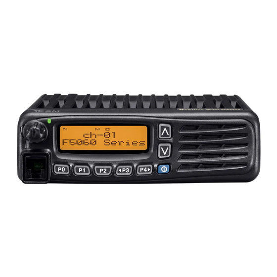
Icom IC-F6061 Service Manual
Uhf transceivers
Hide thumbs
Also See for IC-F6061:
- Service manual (9 pages) ,
- Operating manual (50 pages) ,
- Instruction manual (32 pages)
Table of Contents
Advertisement
Advertisement
Table of Contents

Subscribe to Our Youtube Channel
Related Manuals for Icom IC-F6061


Summary of Contents for Icom IC-F6061
- Page 1 UHF TRANSCEVERS S-14324XZ-C1 Feb. 2007...
- Page 2 8. READ the instructions of test equipment thoroughly before connecting equipment to the transceiver. Icom, Icom Inc. and logo are registered trademarks of Icom Incorporated (Japan) in the United States, the United Kingdom, Germany, France, Spain, Russia and/or other countries.
-
Page 3: Table Of Contents
CONTENTS SECTION SPECIFICATIONS SECTION INSIDE VIEWS SECTION DISASSEMBLY INSTRUCTIONS SECTION OPTIONAL UNITS INSTALLATION SECTION CIRCUIT DESCRIPITON RECEIVER CIRCUITS............5-1 TRANSMITTER CIRCUITS . -
Page 4: Specifications
SECTION 1 SPECIFICATIONS [USA] [EXP] [EUR] • Frequency coverage 400–470 MHz [USA-01] 400–470 MHz [EXP-01] 400–470 MHz 450–512 MHz [USA-02] 450–520 MHz EXP-02] • Type of emission Wide 16K0F3E (25.0 kHz) Middle – 14K0F3E (20.0 kHz) 11K0F3E (12.5 kHz) 11K0F7E/D (12.5 kHz) 8K50F3E (12.5 kHz) Narrow 8K10F1E/D (12.5 kHz) -
Page 5: Inside Views
SECTION 2 INSIDE VIEWS • FRONT UNIT FRONT CPU (IC503: HD64F3687) LCD DRIVER (IC501: S1D15206F) FRONT CPU CLOCK (X501: CR-764) • MAIN UNIT AF SWITCH/AMP BBIC CLOCK (IC1: NJM12902V) (X2: CR-765) IF IC (IC170: TA31136FNG) REF OSC (X1: CR-826) PLL IC (IC4: LMX2352TM) CPU CLOCK (X5: CR-764) - Page 6 SECTION 3 DISASSEMBLY INSTRUCTION 1. Removing the front panel 2. Removing the MAIN UNIT q Turn the transceiver’s power OFF, then disconnect the DC q Unscrew 7 screws A, and unsolder 3 points B. power cable w Unscrew the 4 bottom screws, then remove the bottom cover from the transceiver in the direction of the arrow.
-
Page 7: Section 4 Optional Units Installation
SECTION 4 OPTIONAL UNITS INSTALLATION BEFORE INSTALLING OPTIONAL UNITS A sponge with an adhesive strip has been added to optional units (UT-96R, UT-108R, UT-109R, UT-110R, UT-119R, UT-119H, UT-124, UT-124R). Remove the bottom protective papar, and attach the sponge to the specifi ed position on the optional units as below. - Page 8 Optional UT-96R or UT-119H installation Install the optional UT-96R or UT-119H unit as follows: q Turn the power OFF, then disconnect the DC power cable. w Unscrew the 4 cover screws, then remove the bottom cover. Sponge Front panel e Install the UT-96R to J1 and the UT-119H to J2 as shown in the diagram below.
-
Page 9: Receiver Circuits
SECTION 5 CIRCUIT DESCRIPTION The 1st IF signal from the 1st IF amplifier (Q12) is applied 5-1 RECEIVER CIRCUITS to the IF IC (IC5, pin 16). The applied signal is converted RF CIRCUITS into the 2nd IF signal by being mixed with the 2nd LO signal The antenna switching circuit toggles between the receive from X1 via tripler (Q3, L3, L2, C32−C35). -
Page 10: Transmitter Circuits
The processed AF signals from the base band IC (IC2) are 5-2 TRANSMITTER CIRCUITS passed through the AF mute switch (IC8, pins 3, 4) and D/A MICROPHONE AMPLIFIER CIRCUITS converter (IC6, pins 15, 16) for level adjustment. The level The AF signals from the microphone (MIC signals) are adjusted AF signals are amplified by AF amplifier (IC22). -
Page 11: Frequency Synthesizer Circuits
TX POWER AMPLIFIERS APC CIRCUIT The transmit signal from the TX VCO is amplified to the The APC (Automatic Power Control) circuit prevents the transmit output level by the transmit amplifi ers. transition of the transmit output power level which is caused by load mismatching or heat effect, etc. -
Page 12: Power Supply Circuits
PLL IC The phase difference is output from pin 4 as a pulse type The PLL circuit provides stable oscillation of the transmit signal after being passed through the internal charge pump. frequency and receive 1st LO frequency. The PLL output The output signal is converted into the DC voltage (lock frequency is controlled by the divided ratio (N-data) from the voltage) by passing through the loop filter (Q8, Q9). -
Page 13: Port Allocations
5-5 PORT ALLOCATIONS Port Description Name • CPU (MAIN UNIT; IC14) Outputs CPU clock frequency shift signal to the CPU Port CSFT Description clock oscillator (X2, D38). Name Outputs CTCSS/DTCS select signal to the CTCSS/ DUSE DSDA Outputs serial data to the D/A converter (IC20, pin 6). DTCS switch (Q34). -
Page 14: Section 6 Adjustment Procedures
[Next>] to install the software to the destination folder. (e.g. items as below. C:\Program Files\Icom\CS-F5060 ADJ) t Set or modify adjustment data as specifi ed. y After the installation is completed, the “InstallShield Wiz- ard Complete”... - Page 15 SP (4 Ω) the antenna connector. to the antenna connector OPC-1122U (USB type) to an RS-232C port JIG CABLE RS-232C cable (straight) IC-F6061 to the IC-F6062 [MICROPHONE CONNECTOR] IC-F6063 AC millivoltmeter JIG CABLE Audio generator Add a jumper wire here...
- Page 16 • ADJUSTMENT SOFTWARE WINDOW Transmit output power Modulation balance FM deviation CTCSS/DTCS deviation Squelch level Reference frequency RX sensitivity (Auto.) RX sensitivity (Manu.) PLL lock Voltage (Adjustment) PLL lock Voltage (Preset) S-meter FM deviation (Narrow) FM deviation (Middle) *; DO NOT put the cursor on these items and push the [ENTER] key.
-
Page 17: Frequency Adjustment
6-2 FREQUENCY ADJUSTMENT Select an adjustment item using [↑] / [↓] keys, then set to the specifi ed value using [←] / [→] keys on the connected PC’s keyboard. ADJUSTMENT ADJUSTMENT CONDITION UNIT OPERATION VALUE PLL LOCK 1 Set the preset value of [LV (RX1)], [LV RX2] to “204 [4 V]”, and [LV TX] to “39 [0.76 V]” on the PC screen. VOLTAGE 2 •... -
Page 18: Transmit Adjustment
6-3 TRANSMIT ADJUSTMENT Select an adjustment item using [↑] / [↓] keys, then set to the specifi ed value using [←] / [→] keys on the connected PC’s keyboard. ADJUSTMENT ADJUSTMENT CONDITION UNIT OPERATION VALUE OUTPUT 1 • Channel : CH 5 Rear Connect an RF power meter to 45 W [USA]... -
Page 19: Receive Adjustment
6-4 RECEIVE ADJUSTMENT Select an adjustment item using [↑] / [↓] keys, then set to the specifi ed value using [←] / [→] keys on the connected PC’s keyboard. ADJUSTMENT ADJUSTMENT CONDITION UNIT LOCATION VALUE RECEIVE NOTE: “RECEIVE SENSITIVITY” must be adjusted before “S-METER.” Otherwise, “S-METER” will not be SENSITIVITY adjusted properly. -
Page 20: Parts List
SECTION 7 PARTS LIST [FRONT UNIT] [FRONT UNIT] ORDER ORDER DESCRIPTION DESCRIPTION LOCATION LOCATION IC501 1130009121 S.IC S1D15206F00A200 33.1/19.5 C503 4030016930 S.CER ECJ0EB1A104K 42.7/30.2 IC502 1110005771 S.IC S-80942CNMC-G9CT2G 61.4/9.7 C504 4030016930 S.CER ECJ0EB1A104K 43.6/30.2 IC503 1140010771 S.IC HD64F3687FPV 62.1/25.2 C505 4030016930 S.CER ECJ0EB1A104K 44.5/30.2 IC504... - Page 21 [MAIN UNIT] [MAIN UNIT] ORDER ORDER DESCRIPTION DESCRIPTION LOCATION LOCATION 1110005340 S.IC NJM12902V-TE1-#ZZZB 82.3/12.9 1790001260 S.DIO MA2S077-(TX) 125/38.9 1110006221 S.IC AK2346P-E2/P 44.7/11.7 1750000581 S.DIO 1SV307 (TPH3,F) 50.8/47.1 1140013200 S.IC CD4053BPWR 58.7/9.3 1790001260 S.DIO MA2S077-(TX) 48.3/46 1130010100 S.IC LMX2352TMX/NOPB 83.3/46 1750000711 S.VCP HVC350BTRF-E 14.1/36.1 1110003491 S.IC TA31136FNG (D,EL)
- Page 22 [MAIN UNIT] [MAIN UNIT] ORDER ORDER DESCRIPTION DESCRIPTION LOCATION LOCATION 6200010150 S.COL AS080340-15N 14.3/60.3 7030005240 S.RES ERJ2GEJ 473 X (47 k) 63.7/18 6200010150 S.COL AS080340-15N 10.3/82.4 R100 7010006920 RES PSD1/2 1 K 80.1/33.9 6200002861 S.COL NLV25T-4R7J 111.3/55.1 R101 7030007280 S.RES ERJ2GEJ 331 X (330) 80.1/32.9 6200005011 S.COL NLV25T-100J 40.1/41.6...
- Page 23 [MAIN UNIT] [MAIN UNIT] ORDER ORDER DESCRIPTION DESCRIPTION LOCATION LOCATION R207 7030005050 S.RES ERJ2GEJ 103 X (10 k) 120.3/37 R314 7030007340 S.RES ERJ2GEJ 153 X (15 k) 10/55.3 R208 7030005050 S.RES ERJ2GEJ 103 X (10 k) 121/37.7 R315 7030000220 S.RES MCR10EZHJ 47 (470) 3/61.6 R209 7410001130 S.ARY...
- Page 24 [MAIN UNIT] [MAIN UNIT] ORDER ORDER DESCRIPTION DESCRIPTION LOCATION LOCATION 4030017570 S.CER ECJ0EC1H040B 32/15.4 C151 4030016930 S.CER ECJ0EB1A104K 111.1/46.3 4030017590 S.CER ECJ0EC1H070C 30.8/15.9 C152 4030016930 S.CER ECJ0EB1A104K 108.5/35.7 4030016930 S.CER ECJ0EB1A104K 22.9/15 C153 4030017460 S.CER ECJ0EB1E102K 110.3/35.6 4030017360 S.CER ECJ0EC1H030B 28/15.4 C154 4030018860 S.CER ECJ0EB0J105K...
- Page 25 [MAIN UNIT] [MAIN UNIT] ORDER ORDER DESCRIPTION DESCRIPTION LOCATION LOCATION C236 4030017580 S.CER ECJ0EC1H060C [Low] 44.2/44.6 C327 4030017460 S.CER ECJ0EB1E102K 83.9/79.3 4030017620 S.CER ECJ0EC1H100C [High] 44.2/44.6 C328 4030017420 S.CER ECJ0EC1H470J 82.9/79.3 C237 4030017620 S.CER ECJ0EC1H100C 45.1/46 C329 4030017400 S.CER ECJ0EC1H220J 81.9/79.3 C239 4030017350 S.CER ECJ0EC1H020B...
-
Page 26: Connect Unit
[MAIN UNIT] ORDER DESCRIPTION LOCATION C433 4030017460 S.CER ECJ0EB1E102K 119.4/70.8 C435 4030016930 S.CER ECJ0EB1A104K 8.9/7.8 C436 4030016930 S.CER ECJ0EB1A104K 56/38.5 6510025220 S.CNR AXK540145J 124.5/9.7 6510025220 S.CNR AXK540145J 101.5/9.7 6510021301 S.CNR 52365-1071 90.3/62.6 6510021301 S.CNR 52365-1071 6510023091 S.CNR 20FLT-SM2-TB (LF) (SN) 108.3/83.2 6450000140 CNR HSJ0807-01-010... - Page 27 SECTION 8 MECHANICAL PARTS [CHASSIS PARTS] [CONNECT UNIT] ORDER ORDER DESCRIPTION QTY. DESCRIPTION QTY. J602 6510023210 CD6125SA1J0 6510004880 MR-DSE-01 W601 8900012711 OPC-1297A 8010020540 2979 CHASSIS 8930070860 O-RING (BM) 8110008960 2979 COVER 8930070920 2979 D-SUB PLATE 8510018090 2979 FILTER CASE 8930048550 2177 CLIP [ACCESSORIES] 8810008661 Screw BT B0 3X8 NI-ZC3 (BT) MP10...
- Page 28 J602 (CN) • EXPLODED VIEW MP13 (C) MP4 (F) J602 (CN) 161 ( MP1 (C) CONNECTOR UNIT MP10 (C) W601 (CN) J1 (C) MP2 (C) Unit: mm (inch) 160 ( MP508 (F) MP517 (F) W501 (F) R546 (F) MP507 (F) MP14 (C) MP503 (F) IC15 (M)
- Page 29 SECTION 9 BOARD LAYOUTS • CONNECT UNIT (TOP VIEW) • MAIN UNIT (TOP VIEW) • HM-152 (TOP VIEW) DASW PFMF EMPH OPT3 OPT2 CIRQ OPT1 SIGO BUSY AFOUT DISC RMUT BEPO MCIN AFON MMUTI MCOT PTTO PTTI OPT3 OPT2 CIRQ OPT1 DAFO VREF...
- Page 30 • MAIN UNIT (BOTTOM VIEW) • HM-152 (BOTTOM VIEW) B6360A J601 PGI1 BUSY EPTTO EXMOD DISC HORNO MMUTO DIMO MMUT HANGO 20 • FRONT UNIT (BOTTOM VIEW) W502 SP501 IC15 W503 S-14324XH-P2 Printed in Japan © 2007 Icom Inc. 9 - 2...
- Page 31 SECTION 10 BLOCK DIAGRAM MAIN UNIT RIPPLE 2SC4116 D9:HVC383B 400-520MHz Q17:2SC4226 2SK880 RXVCO 2 HVC350B LVIN BUFF RLVA IC15 RA30H4047M RA30H4452M D38 UM9401F (25W ) HVC350B D11:HVC383B D24 1SV307 RA55H4047M D39 L407CD (45W) D49,D51 2SC5107 2SC335 6 2SC5107 Q18:2SC4226 2SC5107 D25 MA2S077 RA55H4452M MA728...
- Page 32 SECTION 11 VOLTAGE DIAGRAM • FRONT UNIT Q 504 2SC411 6 POSW DS502 R507 KYUP R508 CL-165HR DTC114TU Q501 Q505 Q507 KYDN DTC114TU DTC114TU DTC114TU Q502 LIGT1 LIGT2 J501 P8 6 P8 6 FMDA P8 7 P8 7 M FDA P8 5 P8 5 FRONT UNIT...
- Page 33 MAIN UNIT (1) VCO8V TEM P 2SC4116 R142 *C133 *C161 2SC4226 *C134 C190 2SK880 NJM12902V 1.2U HVC350B 0.5P 330K IC 1 1.2K R265 1 VCON 330K 2 GND *R168 NJM12902V 0.33 SVA 0.47 SVA *C426 15.3MHZ *D38 1.2U *C257 AS080340 R101 *C268 *L30...
- Page 34 MAIN UNIT (2) R311 *C336 AS080340 AS080340 AS080340 C342 0.001 AS080340 R315 C347 R307 MA728 MA728 0.3P 1SS375 *R28 9 *Q33 UNR9213J SP JACK DAN222 C384 HSJ0807-01-010 IC21 LA4425A R325 UNR9213J DTC363EK MA2S111 DAN222 C38 9 R350 0. 1 C387 C40 0 470P 0.
- Page 35 SECTION 12 HM-152 • ELECTRIC PARTS • VOLTAGE DIAGRAM [MAIN UNIT] ORDER 7.57V 8.00V DESCRIPTION 7030011410 S.RES ERJ3GE YJ 222 7030011410 S.RES ERJ3GE YJ 222 7030011420 S.RES ERJ3GE YJ 562 7030011410 S.RES ERJ3GE YJ 222 HM-152 7.14V CLONE 4510009230 S.ELE EEE1HA010SR 4030018990 S.CER C1608 JB 1H 102K...
- Page 37 S-14324XZ-C1 1-1-32, Kamiminami, Hirano-ku, Osaka 547-0003, Japan © 2007 Icom Inc.
Need help?
Do you have a question about the IC-F6061 and is the answer not in the manual?
Questions and answers