Sign In
Upload
Download
Table of Contents
Contents
Add to my manuals
Delete from my manuals
Share
URL of this page:
HTML Link:
Bookmark this page
Add
Manual will be automatically added to "My Manuals"
Print this page
×
Bookmark added
×
Added to my manuals
Manuals
Brands
Icom Manuals
Transceiver
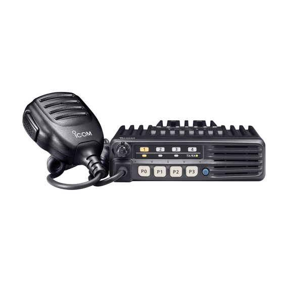
IC-F6012
Service manual
Icom IC-F6012 Service Manual
Hide thumbs
Also See for IC-F6012
:
Instruction manual
(24 pages)
1
2
Table Of Contents
3
4
5
6
7
8
9
10
11
12
13
14
15
16
17
18
19
20
21
22
23
24
25
26
27
28
29
30
31
32
33
34
35
36
37
38
39
40
41
42
43
page
of
43
Go
/
43
Contents
Table of Contents
Bookmarks
Table of Contents
Table of Contents
Specifications
Section 2 Inside Views
Section 3 Disassembly Instruction
Section 4 Optional Products Installation
Receiver Circuits
Transmitter Circuits
Frequency Synthesizer Circuits
Voltage Diagrams
Port Allocations
Preparation
Frequency Adjustment
Transmit Adjustment
Receive Adjustment
Parts List
Front Unit
Advertisement
Quick Links
1
Specifications
2
Section 2 Inside Views
3
Section 4 Optional Products Installation
4
Receiver Circuits
5
Voltage Diagrams
6
Port Allocations
7
Preparation
8
Frequency Adjustment
Download this manual
See also:
Instruction Manual
Enlarged version
UHF MOBILE TRANSCEIVERS
S-14716XZ-C1
Mar. 2011
Table of
Contents
Previous
Page
Next
Page
1
2
3
4
5
Advertisement
Table of Contents
Need help?
Do you have a question about the IC-F6012 and is the answer not in the manual?
Ask a question
Questions and answers
Related Manuals for Icom IC-F6012
Transceiver Icom iC-F5012 Instruction Manual
Vhf mobile transceiver/uhf mobile transceiver (24 pages)
Transceiver Icom IC-F6013H Instruction Manual
Ic-f5010 series, ic-f6010 series vhf/uhf mobile transceivers (26 pages)
Transceiver Icom IC-F5011 Instructions
Ic-f5010 series, ic-f6010 series vhf mobile transceiver, uhf mobile transceiver (2 pages)
Transceiver ICOM IC-F5010 series Instruction Manual
Vhf/uhf mobile transceiver (24 pages)
Transceiver ICOM IC-F5020 Series Insrtuction Manual
Vhf/uhf mobile transceivers (24 pages)
Transceiver Icom IC-F5020 Series Instruction Manual
Vhf mobile transceivers (9 pages)
Transceiver ICOM IC-F6061 Service Manual
Uhf transceivers (37 pages)
Transceiver Icom IC-F6061 Service Manual
(9 pages)
Transceiver ICOM IC-F5022 Instruction Manual
Vhf/uhf mobile transceiver mdc 1200 compatible (24 pages)
Transceiver ICOM IC-F6022 Instruction Manual
Uhf/vhf mobile transceiver mdc 1200 compatible (24 pages)
Transceiver ICOM IC-F5062D Instruction Manual
Uhf/vhf dpmr mobile transceiver (32 pages)
Transceiver ICOM IC-F5062D Instructions
(2 pages)
Transceiver Icom IC-F5062 Instruction Manual
Vhf mobile transceivers; uhf mobile transceivers (9 pages)
Transceiver Icom IC-F50V Instruction Manual
Vhf/uhf transceiver (48 pages)
Transceiver ICOM IC-F50V SERIES Operating Manual
(20 pages)
Transceiver Icom IC-F5060 SERIES Instruction Manual
(32 pages)
This manual is also suitable for:
Ic-f6011
Ic-f6013
Ic-f6013h
Table of Contents
Print
Rename the bookmark
Delete bookmark?
Delete from my manuals?
Login
Sign In
OR
Sign in with Facebook
Sign in with Google
Upload manual
Upload from disk
Upload from URL


Need help?
Do you have a question about the IC-F6012 and is the answer not in the manual?
Questions and answers