Table of Contents
Advertisement
Advertisement
Table of Contents

Related Manuals for Stanford Research Systems SR530


Summary of Contents for Stanford Research Systems SR530
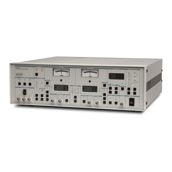
- Page 1 MODEL SR530 LOCK-IN AMPLIFIER 1290-D Reamwood Avenue Sunnyvale, CA 94089 U.S.A. Phone: (408) 744-9040 • Fax: (408) 744-9049 Email: info@thinkSRS.com • www.thinkSRS.com Copyright © 1997, 2001, 2005, 2013 Stanford Research Systems, Inc. All Rights Reserved Rev. 2.4 (11/2013)
-
Page 3: Table Of Contents
Noise Measurements Default Settings Ratio Capability Computer Interfaces Rear Panel Internal Oscillator AC Power GPIB (IEEE-488) Connector SR530 Block Diagram RS232 Connector Block Diagram Signal Monitor Output Signal Channel Pre-Amp Connector Reference Channel A/D Inputs and D/A Outputs Phase-Sensitive Detector... - Page 4 IBM PC, Microsoft Basic, via GPIB Circuit Description Introduction HP-85, HP Basic, via HPIB Signal Amplifier Current Amplifier Documentation Notch Filters Parts List, Oscillator Board Bandpass Filter Parts List, Main Board Reference Oscillator Parts List, Front Panel Board PSD, LP Filters and DC Amplifier Parts List, Quad Board Analog Output Parts List, Miscellaneous...
-
Page 5: Safety And Preparation For Use
LINE VOLTAGE SELECTION FURNISHED ACCESSORIES The SR530 operates from a 100V, 120V, 220V, or - Power Cord 240V nominal ac power source having a line - Operating Manual frequency of 50 or 60 Hz. -
Page 7: Specifications
SR530 Specification Summary General Power 100, 120, 220, 240 VAC (50/60 Hz); 35 Watts Max Mechanical 17" x 17" x 5.25" (Rack Mount Included) 16 lbs. Warranty Two years parts and labor. Signal Channel Inputs Voltage: Single-ended or True Differential... - Page 8 Acquisition Time 25 Sec at 1 Hz 6 Sec at 10 Hz 2 Sec at 10 kHz Slew Rate 1 decade per 10 S at 1 kHz Phase Control 90° shifts Fine shifts in 0.025° steps Phase Noise 0.01° rms at 1 kHz, 100 msec, 12 dB TC Phase Drift 0.1°/°C Phase Error...
-
Page 9: Front Panel Summary
Front Panel Summary Signal Inputs Single Ended (A), True Differential (A-B), or Current (I) Signal Filters Bandpass: Q-of-5 Auto-tracking filter (In or Out) Line Notch: Q-of-10 Notch Filter at line frequency (In or Out) 2XLine Notch: Q-of-10 Notch Filter at twice line frequency (In or Out) Sensitivity Full scale sensitivity from 100 nV to 500 mV RMS for voltage inputs or from 100 fA to 500 nA RMS for current inputs. - Page 10 Phase Controls Adjust phase in smoothly accelerating 0.025° steps, or by 90° steps. Press both 90° buttons to zero the phase. Reference LCD Display reference phase setting or reference frequency Time Constants Pre-filter has time constants from 1 mS to 100 S (6 dB/Octave) Post-filter has time constants of 0, 0.1 or 1.0 S (6 dB/Octave) ENBW Equivalent Noise Bandwidth.
-
Page 11: Abridged Command List
Abridged Command List Return X Offset Status OX 0 Turn off X Offset Auto offset X OX 1,v Turn on X Offset, v = offset Auto offset Y Return Y Offset Status Auto offset R OY 0 Turn off Y Offset Auto phase OY 1,v Turn on Y Offset, v = offset... -
Page 12: Status Byte Definition
Eight data bits are always sent, regardless of the parity setting. The most significant bit is always zero. Example: Bit 1 'down' and all others 'up' for RS232 communication at 9600 baud, no parity, two stop bits, and no echo or prompts by the SR530. -
Page 13: Front Panel
allowable signals at the inputs. The notch SR510 Guide to Operation frequencies are set at the factory to either 50 Hz Front Panel or 60 Hz. The user can adjust these frequencies. (See the Maintenance and Repair section for alignment details.) These filters precede the bandpass filter in the signal amplifier. -
Page 14: Dynamic Reserve
ACT indicates activity on the computer interfaces. This LED blinks every time a character is received The dynamic reserve and output stability of each or transmitted by the SR530. setting are shown below. REM indicates that the unit is in the remote state... -
Page 15: R Output
display CH1 The left hand analog meter always displays the setting output expand? offset? (RCOSØ) CHANNEL 1 OUTPUT voltage. Accuracy is 2% of full scale. X+X ofst yes X+X ofst The CHANNEL 1 LCD display provides a read-out XOFST X ofst X ofst of the displayed parameter in real units. -
Page 16: Expand Channel 1
in magnitude to the selected sensitivity which is in to ON) sets the offset to the previously entered phase with the reference oscillator will generate a value. 10V output. The output impedance is <1Ω and the If an attempt is made to advance the offset value output current is limited to 20 mA. -
Page 17: Output Channel 2
possible. If R is less than 0.5% of full scale, the The CHANNEL 2 LCD display provides a read-out phase output defaults to zero degrees. of the displayed parameter in real units. The scale of the displayed quantity is indicated by the four The Phase Output may not be expanded and the scale LED's to the right of the display. -
Page 18: Expand Channel 2
down, the offset advances in larger and larger Y (RSINØ) Output increments, the largest increment being 10% of full scale. When the offset is turned OFF the applied The analog output, Y+Y ofst , is available at the Y offset returns to zero but the offset value is not (RSINØ) BNC connector. -
Page 19: Reference Mode
In many servo applications, no time constant is case, the reference oscillator has a maximum needed. The SR530 may be modified to reduce the output time constant to about 20 µS. Contact frequency of 100 KHz, thus, when in the 2f mode, the reference input frequency may not exceed 50 the factory for details. -
Page 20: Power Switch
Whenever default values are used at power up, The SR530 always powers up in the LOCAL the red ERR LED will turn on for about 3 seconds. mode. -
Page 21: Rear Panel
The input impedance is 1 MΩ. A digitization can be performed in about 3 mS but the result may The SR530 has an IEEE 488 (GPIB) interface built take longer to transmit over the interface being in. The GPIB address is set using SW1 located to used. - Page 22 the REF OUTPUT on the rear panel to the REF 2) If the VCO INPUT is left open, then the INPUT on the front panel. The REF OUTPUT is a oscillator will run at the top of its range (i.e. 10 Hz, 1 KHz, or 100 KHz).
-
Page 23: Communications
There are also two programmable analog output Values returned by the SR530 are sent as a string ports available to provide general purpose control of ASCII characters terminated usually by carriage voltages. -
Page 24: Rs232 Echo Feature
G<cr>. The response should be 24 meaning that the sensitivity is at the 24th setting or In order to allow the SR530 to be operated from a 500 mV. Change the sensitivity by typing terminal, an echo feature has been included which G19<cr>. -
Page 25: Command List
Dyn Res SR530 Command List NORM The leading letters in each command sequence HIGH specify the command. The rest of the sequence consists of parameters. Multiple parameters are Note that not all dynamic reserve settings are separated by a comma. Those parameters shown allowed at every sensitivity. - Page 26 "0", the selected filter is taken out. If n is absent, The J command sets the RS232 end-of-record the status of the selected filter is returned. characters sent by the SR530 to those specified by the decimal ASCII codes n1-n4. If no argument M {n} is included, the end-of-record sequence returns to If n is "1", the M command sets the reference...
- Page 27 The W command sets and reads the RS232 parameters shown on the Channel 1 and 2 analog character wait interval. If n is included, the SR530 meters, output digital displays, and output BNC's. will wait nx4 mS between characters sent over the If n is absent, the displayed parameter is returned.
-
Page 28: Status Byte
Bit 6 RS232 interface. SRQ. This bit is set if the SR530 has generated an SRQ on the GPIB interface. This bit is reset Status Byte after the SR530 has been serial polled. This bit is set only for status reads via a serial poll, ie., Bit 6... -
Page 29: Reset Command
The Z command resets the unit to its default state. not pass it between the SR530 and the The default front panel settings are listed in the computer, or, your computer is not DEFAULTS section of the Guide to Operations. -
Page 30: Data Communications Equipment
J command, the terminating sequence returns (DCE) to the default (echo on: <cr><lf>; echo off: <cr>). The SR530 is configured as DCE so that it may be The J command does not affect the terminating connected directly to a terminal. If the SR530 is to character (<cr>) required at the end of commands... -
Page 31: Serial Polls And Srq's
GPIB and will slow down the GPIB data rate in this mode. The status byte sent by the SR530 when it is serial (Use the W0 command to allow the RS232 polled is the same status byte which is read using interface to run at full speed, otherwise, the GPIB the Y command (except for bit 6, SRQ). -
Page 32: Measurement Example
The Lock-in Technique A Measurement Example The Lock-in technique is used to detect and Suppose we wish to measure the resistance of a measure very small ac signals. A Lock-in amplifier material, and we have the restriction that we must can make accurate measurements of small signals not dissipate very much power in the sample. -
Page 33: Understanding The Specifications
The magnitude output is given by, the phase shift error. The SR530's 1° phase accuracy will not make a significant contribution to R = {(V psd1 )2 + (V psd2 ) 2 } 1/2 ~ V s the measurement error. -
Page 34: Dynamic Reserve
appears on both the A & B inputs will not be In the first method, the lock-in uses the A input in a perfectly cancelled: the common mode rejection 'quasi-differential' mode. Here, the lock-in detects ratio (CMRR) specifies the degree of cancellation. the signal as the voltage between the center and For low frequencies the CMRR of 100 dB indicates outer conductors of the A input. -
Page 35: Notch Filters
In many servo applications, no output filtering is use the bandpass filter and select a low dynamic needed. In this case, the SR530 may be modified to reduce the output time constant to about 20 µS. reserve setting in order to achieve a better output stability. -
Page 36: Sr530 Block Diagram
Several new concepts are used to simplify the amplifiers or heterodyning techniques. All of these design of SR530 lock-in amplifier. In addition to 'fix-ups' had drawbacks, including phase and implementing recent advances in linear integrated... -
Page 37: Signal Channel
DC Amplifiers and System Gain are placed in the instrument's read-only memory. The SR530 has only one-fifth of the analog Dc amplifiers amplify and offset the outputs of the trimming components that are found in older two low pass filters. -
Page 38: Circuit Description Introduction
1-2-5-10 attenuator. The signal is then amplified by 2/2 U102. Input overload is The SR530 has eight main circuit areas: the signal sensed through diodes D101-D104. amplifier, the reference oscillator, the demodulator, the analog output and controls, the front panel, the... -
Page 39: Reference Oscillator
U204, and U205 are analog switches which select phase or quadrature relationship between the the feedback capacitors for the 5 decades of two VCO's. Thus, the output of the second VCO operation. The two halves of U202 are matched can be shifted from -5 to 185 deg from the transconductance amplifiers operating as reference. -
Page 40: Analog Output
U419. Analog switch U418 selects the time constant used to program the band pass filter and the and gain. The full scale output of U418 is 5 volts. reference oscillator phase shift. One output is subtracted from the lock-in output in U508 to The quadrature demodulator and low pass amplifiers provide a variable offset and another is the rms are identical to that described above. -
Page 41: Rs232 Interface
or, generates the gate pulse during which reference Internal Oscillator pulses are counted. The internal oscillator is on a small circuit board I/O addresses are decoded by U705, U706, and attached to the rear panel of the instrument. U707. The microprocessor controls the lock-in Local regulators, Q1 and Q2, provide power to functions through I/O ports U714-U721. -
Page 42: Calibration And Repair
minimize the 500 Hz output. Adjust P403 at location Calibration and Repair C2 to minimize the 30 Hz output. Now set the both time constants to 1S. Adjust P404 This section details calibration of the instrument. at location F4 to zero the output. This adjustment Calibration should be done only by a qualified has a range of 20% of full scale on the HIGH electronics technician. -
Page 43: Line Notch Filter Adjustment
The CMRR is adjusted by the single turn Replacing the Front-End Transistors potentiometer located at A1 under the single hole at the front of the signal shield. (The shield Both the voltage and current front end transistors is the aluminum box on the left side of the main (Q101 and Q102) are 2N6485 (IMF6485) dual board). -
Page 44: Appendix A: Noise Sources And Cures
And Others. Other noise sources include flicker Appendix A: noise found in vacuum tubes, and generation and Noise Sources and Cures recombination noise found in semiconductors. All of these noise sources are incoherent. Thus, the Noise, random and uncorrelated fluctuations of total noise is the square root of the sum of the electronic signals, finds its way into experiments squares of all the incoherent noise sources. -
Page 45: Capacitive Coupling
Capacitive Coupling. A voltage on a nearby Inductive Coupling. Here noise couples to the piece of apparatus (or operator) can couple to a experiment via a magnetic field: detector via a stray capacitance. Although C stray may be very small, the coupled in noise may still be larger than a weak experimental signal. -
Page 46: Ground Loops
Resistive Coupling (or 'Ground Loops'). Microphonics provides a path for mechanical noise Currents through common connections can give to appear as electrical noise in a circuit or rise to noise voltages. experiment. Consider the simple circuit below: The capacitance of a coaxial cable is a function of its geometry so mechanical vibrations will cause the cable capacitance to vary with time. -
Page 47: Using Control Lines
If the terminal responds to a control Introduction to the RS232 line, it will believe that the SR530 is not ready to accept data (because the line is not passed in this example) and will therefore not send any data. -
Page 48: Stop Bits
To use as a debugging tool, attach the hook clip to either pin 2 or pin 3 of the RS232 cable on the SR530 to show either data sent from the Computer or the SR530. -
Page 49: Introduction To The Gpib
Data Bus: There are eight data lines which use Appendix C: negative logic and pass the bits of each byte in Introduction to the GPIB parallel. General Interface Lines: These five lines operate The IEEE-488 Standard specifies the voltage independently of the handshake lines and use levels, handshake requirements, timing, negative logic. -
Page 50: Appendix D: Program Examples
EXAMPLE PROGRAM TO READ THE SR510 OUTPUT AND RAMP THE X6 ANALOG OUTPUT 20 ′ USING IBM PC BASICA AND THE COM1: RS232 PORT. 30 ′ THE RAMP ON X6 CAN BE WATCHED BY SETTING THE SR530 DISPLAY TO A/D. 40 ′ 50 ′ 60 ′... - Page 51 19.2 kbaud from FORTRAN programs. Only two wires between the IBM PC's ASYNC port and the SR530 are needed (pins #2 & #3 of the RS232), but pins 5,6,8 and 20 should be connected together on the connector at the IBM end.
- Page 52 call rxstr(str2) convert string variable into real variable v1 and v2 read (str1,1000) v1 read (str2,1000) v2 1000 format (bn,f10.0) print results to screen write(*,2000) v1, v2 format(′ Channel 1=′,G10.3,3x, ′Channel 2=′,G10.3) 2000 ramp x6 by 2.5 mV x6 = x6 + .0025 if (x6.gt.10) x6 = 0.0 make x6 command string write (str3,3000) x6...
- Page 53 Output using Microsoft C v3.0 (large model) and the COM1: port. Set all switches in SW2 to UP on SR530 for 19.2 kbaud. The ramp on x6 can be watched by setting the SR530 display to D/A. main () char str1[20], str2[20], STR3[20];...
- Page 54 txstr (″q2$″); /* read channel 2 output */ rxstr (str2); /* into str2 */ sscanf (str2, ″%f″, &v2); /* scan str2 for a float variable */ x += 0.0025; /* increment x6 output by 2.5 mV */ if (x >= 10) x = 0; sprintf (str3, ″X6,%f$″, x);...
-
Page 55: Ibm Pc, Microsoft Basic, Via Gpib
THE RAMP ON X6 CAN BE MATCHED BY SETTING THE SR530 DISPLAY TO D/A. 50 ′ 60 ′ ON THE SR530 REAR PANEL, SET SWITCHES #4 AND #6 ON SW1 TO DOWN (DEVICE 70 ′ ADDRESS = 23, RS232 ECHO ON) AND SWITCH # 1 ON SW2 TO DOWN (RS232 BAUD 80 ′... - Page 56 460 GOSUB 600 470 ′ ′LOOP FOREVER 480 GOTO 300 490 ′ 500 ′ GET AN ANSWER STRING FROM THE SR530 510 CALL TRANSMIT(LISN$,STATUS%) ′MAKE SR530 A TALKER 520 GOSUB 600 ′INIT ANSWER STRING 530 ANS$=SPACE$(10) ′READ RESULT INTO ANS$...
-
Page 57: Hp-85, Hp Basic, Via Hpib
This program provides an example of an HP85 program using the GPIB interface which could be used to control the lockin amplifier. In this example, the SR530 should be addressed as device #16 by setting the switch bank SW1 per the instructions Page 7. -
Page 58: Documentation
Documentation This section contains the parts lists and schematics for the SR530 lock-in amplifier. The first digit of any part number can be used to locate the schematic diagram for the part. For example, R415 is located on sheet 4 of the... - Page 59 SR530 COMPONENT PARTS LIST Oscillator Board Parts List REF. SRS part# VALUE DESCRIPTION 5-00023-529 Cap, Monolythic Ceramic, 50V, 20%, Z5U 5-00023-529 Cap, Monolythic Ceramic, 50V, 20%, Z5U 5-00102-517 4.7U Capacitor, Tantalum, 35V, 20%, Rad 5-00054-512 .047U Cap, Stacked Metal Film 50V 5% -40/+85c...
-
Page 60: Parts List, Main Board
SR530 COMPONENT PARTS LIST Main Board Parts List REF. SRS part# VALUE DESCRIPTION 3-00062-340 KBP201G/BR-81D Integrated Circuit (Thru-hole Pkg) 3-00062-340 KBP201G/BR-81D Integrated Circuit (Thru-hole Pkg) 6-00001-612 BR-2/3A 2PIN PC Battery C 101 5-00069-513 Capacitor, Mylar/Poly, 50V, 5%, Rad C 102... - Page 61 SR530 COMPONENT PARTS LIST REF. SRS part# VALUE DESCRIPTION C 214 5-00059-512 .47U Cap, Stacked Metal Film 50V 5% -40/+85c C 215 5-00060-512 1.0U Cap, Stacked Metal Film 50V 5% -40/+85c C 216 5-00056-512 Cap, Stacked Metal Film 50V 5% -40/+85c...
- Page 62 SR530 COMPONENT PARTS LIST REF. SRS part# VALUE DESCRIPTION C 410 5-00056-512 Cap, Stacked Metal Film 50V 5% -40/+85c C 411 5-00056-512 Cap, Stacked Metal Film 50V 5% -40/+85c C 412 5-00056-512 Cap, Stacked Metal Film 50V 5% -40/+85c C 413 5-00049-566 .001U...
- Page 63 SR530 COMPONENT PARTS LIST REF. SRS part# VALUE DESCRIPTION C 802 5-00012-501 330P Capacitor, Ceramic Disc, 50V, 10%, SL C 803 5-00012-501 330P Capacitor, Ceramic Disc, 50V, 10%, SL C 804 5-00052-512 .01U Cap, Stacked Metal Film 50V 5% -40/+85c...
- Page 64 SR530 COMPONENT PARTS LIST REF. SRS part# VALUE DESCRIPTION 6-00010-620 4.000 MHZ Crystal D 101 3-00004-301 1N4148 Diode D 102 3-00004-301 1N4148 Diode D 103 3-00004-301 1N4148 Diode D 104 3-00004-301 1N4148 Diode D 105 3-00004-301 1N4148 Diode D 106...
- Page 65 SR530 COMPONENT PARTS LIST REF. SRS part# VALUE DESCRIPTION R 102 4-00033-404 100M Resistor, Carbon Comp, 1/4W, 5% R 103 4-00030-401 Resistor, Carbon Film, 1/4W, 5% R 104 4-00031-401 Resistor, Carbon Film, 1/4W, 5% R 105 4-00031-401 Resistor, Carbon Film, 1/4W, 5%...
- Page 66 SR530 COMPONENT PARTS LIST REF. SRS part# VALUE DESCRIPTION R 162 4-00188-407 4.99K Resistor, Metal Film, 1/8W, 1%, 50PPM R 163 4-00035-401 Resistor, Carbon Film, 1/4W, 5% R 165 4-00215-407 Resistor, Metal Film, 1/8W, 1%, 50PPM R 166 4-00141-407 Resistor, Metal Film, 1/8W, 1%, 50PPM...
- Page 67 SR530 COMPONENT PARTS LIST REF. SRS part# VALUE DESCRIPTION R 307 4-00040-401 Resistor, Carbon Film, 1/4W, 5% R 308 4-00193-407 Resistor, Metal Film, 1/8W, 1%, 50PPM R 309 4-00073-401 330K Resistor, Carbon Film, 1/4W, 5% R 310 4-00021-401 1.0K Resistor, Carbon Film, 1/4W, 5%...
- Page 68 SR530 COMPONENT PARTS LIST REF. SRS part# VALUE DESCRIPTION R 359 4-00045-401 2.0K Resistor, Carbon Film, 1/4W, 5% R 360 4-00032-401 100K Resistor, Carbon Film, 1/4W, 5% R 361 4-00084-401 5.1K Resistor, Carbon Film, 1/4W, 5% R 362 4-00181-407 32.4K...
- Page 69 SR530 COMPONENT PARTS LIST REF. SRS part# VALUE DESCRIPTION R 433 4-00021-401 1.0K Resistor, Carbon Film, 1/4W, 5% R 501 4-00022-401 1.0M Resistor, Carbon Film, 1/4W, 5% R 502 4-00022-401 1.0M Resistor, Carbon Film, 1/4W, 5% R 503 4-00022-401 1.0M...
- Page 70 SR530 COMPONENT PARTS LIST REF. SRS part# VALUE DESCRIPTION R 703 4-00027-401 1.5K Resistor, Carbon Film, 1/4W, 5% R 705 4-00021-401 1.0K Resistor, Carbon Film, 1/4W, 5% R 706 4-00034-401 Resistor, Carbon Film, 1/4W, 5% R 707 4-00034-401 Resistor, Carbon Film, 1/4W, 5%...
- Page 71 SR530 COMPONENT PARTS LIST REF. SRS part# VALUE DESCRIPTION U 118 3-00130-340 5532A Integrated Circuit (Thru-hole Pkg) U 201 3-00087-340 LF347 Integrated Circuit (Thru-hole Pkg) U 202 3-00093-340 LM13600 Integrated Circuit (Thru-hole Pkg) U 203 3-00073-340 CD4052 Integrated Circuit (Thru-hole Pkg)
- Page 72 SR530 COMPONENT PARTS LIST REF. SRS part# VALUE DESCRIPTION U 415 3-00126-335 51A05 Relay U 416 3-00084-340 ICL7650 Integrated Circuit (Thru-hole Pkg) U 417 3-00126-335 51A05 Relay U 418 3-00076-340 DG211 Integrated Circuit (Thru-hole Pkg) U 419 3-00090-340 LF411 Integrated Circuit (Thru-hole Pkg)
- Page 73 SR530 COMPONENT PARTS LIST REF. SRS part# VALUE DESCRIPTION U 807 3-00110-340 MC1489 Integrated Circuit (Thru-hole Pkg) U 808 3-00078-340 DS75160A Integrated Circuit (Thru-hole Pkg) U 809 3-00117-325 78L12 Transistor, TO-92 Package U 810 3-00123-325 79L12 Transistor, TO-92 Package U 811...
-
Page 74: Parts List, Front Panel Board
SR530 COMPONENT PARTS LIST REF. SRS part# VALUE DESCRIPTION 0-00257-000 HANDLE3 Hardware, Misc. 0-00371-026 4-40X3/16PF Screw, Black, All Types 0-00500-000 554808-1 Hardware, Misc. 0-00521-048 3" #18 Wire, #18 UL1015 Strip 3/8 x 3/8 No Tin 0-00526-048 10-1/2" #18 Wire, #18 UL1015 Strip 3/8 x 3/8 No Tin... - Page 75 SR530 COMPONENT PARTS LIST REF. SRS part# VALUE DESCRIPTION DS611 3-00012-306 GREEN LED, Rectangular DS612 3-00012-306 GREEN LED, Rectangular DS613 3-00012-306 GREEN LED, Rectangular DS614 3-00012-306 GREEN LED, Rectangular DS615 3-00012-306 GREEN LED, Rectangular DS616 3-00012-306 GREEN LED, Rectangular DS617...
- Page 76 SR530 COMPONENT PARTS LIST REF. SRS part# VALUE DESCRIPTION DS662 3-00012-306 GREEN LED, Rectangular DS663 3-00012-306 GREEN LED, Rectangular DS664 3-00012-306 GREEN LED, Rectangular DS665 3-00012-306 GREEN LED, Rectangular DS666 3-00012-306 GREEN LED, Rectangular DS667 3-00012-306 GREEN LED, Rectangular DS668...
-
Page 77: Parts List, Quad Board
SR530 COMPONENT PARTS LIST REF. SRS part# VALUE DESCRIPTION RN603 4-00226-425 150X9 Resistor Network SIP 1/4W 2% (Common) RN604 4-00222-425 150X7 Resistor Network SIP 1/4W 2% (Common) U 601 3-00086-340 ICM7211AM Integrated Circuit (Thru-hole Pkg) U 602 3-00086-340 ICM7211AM Integrated Circuit (Thru-hole Pkg) - Page 78 SR530 COMPONENT PARTS LIST REF. SRS part# VALUE DESCRIPTION C 1006 5-00058-512 .33U Cap, Stacked Metal Film 50V 5% -40/+85c C 1007 5-00049-566 .001U Cap, Polyester Film 50V 5% -40/+85c Rad C 1008 5-00003-501 Capacitor, Ceramic Disc, 50V, 10%, SL...
- Page 79 SR530 COMPONENT PARTS LIST REF. SRS part# VALUE DESCRIPTION P 1103 4-00016-445 Pot, Multi-Turn, Side Adjust P 1104 4-00016-445 Pot, Multi-Turn, Side Adjust P 1201 4-00016-445 Pot, Multi-Turn, Side Adjust P 1202 4-00016-445 Pot, Multi-Turn, Side Adjust 7-00040-701 SR522 Printed Circuit Board...
- Page 80 SR530 COMPONENT PARTS LIST REF. SRS part# VALUE DESCRIPTION R 1109 4-00022-401 1.0M Resistor, Carbon Film, 1/4W, 5% R 1110 4-00217-408 1.000K Resistor, Metal Film, 1/8W, 0.1%, 25ppm R 1111 4-00193-407 Resistor, Metal Film, 1/8W, 1%, 50PPM R 1112 4-00217-408 1.000K...
-
Page 81: Parts List, Miscellaneous
SR530 COMPONENT PARTS LIST REF. SRS part# VALUE DESCRIPTION U 1102 3-00091-340 LF412 Integrated Circuit (Thru-hole Pkg) U 1103 3-00090-340 LF411 Integrated Circuit (Thru-hole Pkg) U 1104 3-00106-340 LT1007 Integrated Circuit (Thru-hole Pkg) U 1105 3-00074-340 CD4066 Integrated Circuit (Thru-hole Pkg) - Page 82 SR530 COMPONENT PARTS LIST...
Need help?
Do you have a question about the SR530 and is the answer not in the manual?
Questions and answers