Table of Contents
Advertisement
Quick Links
Advertisement
Table of Contents

Related Manuals for Freescale Semiconductor MPC5668EVB


Summary of Contents for Freescale Semiconductor MPC5668EVB
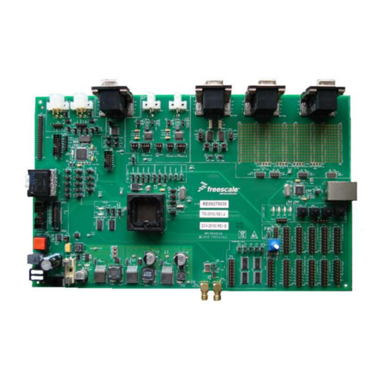
- Page 1 MPC5668EVB Users Manual Revision 0.1 May 2009...
- Page 2 Freescale Semiconductor reserves the right to make changes without further notice to any products herein. Freescale Semiconductor makes no warranty, representation or guarantee...
-
Page 3: Table Of Contents
MPC5668EVB Users Manual Rev 0.1 May 2009 INDEX INTRODUCTION ..............................1 EVB FEATURES ..............................2 CONFIGURATION ..............................3 ........................4 OWER UPPLY ONFIGURATION 3.1.1 Power Supply Connectors ........................4 3.1.2 Power Switch (SW6) ..........................4 3.1.3 Regulator Power Jumpers (J42, J44, J45 and J46) ................5 3.1.4... - Page 4 MPC5668EVB Users Manual Rev 0.1 May 2009 Index of Figures and Tables 3-1 EVB F ..........................3 IGURE UNCTIONAL LOCKS 3-2 2.1 .......................... 4 IGURE OWER ONNECTOR 3-3 2-L ........................4 IGURE EVER OWER ONNECTOR 3-4. P ..........................6 IGURE...
-
Page 5: Mpc5668Evb Users Manual Rev 0.1 May
May 2009 1. Introduction This user’s manual details the setup and configuration of the Freescale Semiconductor MPC5668 Evaluation Board (hereafter referred to as the EVB). The EVB is intended to provide a mechanism for easy customer evaluation of the MPC5668 family of microprocessors, and to facilitate hardware and software development. -
Page 6: Evb Features
MPC5668EVB Users Manual Rev 0.1 May 2009 2. EVB Features The EVB provides the following key features: MCU Socket supporting the 208BGA production package and the 256BGA development package. • Single 12-14V external power supply input with on-board regulators to provide all of the necessary •... -
Page 7: Configuration
MPC5668EVB Users Manual Rev 0.1 May 2009 3. Configuration This section details the configuration of each of the EVB functional blocks. Throughout this document, all of the default jumper and switch settings are clearly marked with “(D)” and are shown in blue text. -
Page 8: Power Supply Configuration
MPC5668EVB Users Manual Rev 0.1 May 2009 Power supply 3.1 Power Supply Configuration section is located in the bottom left area of the EVB The EVB requires an external power supply voltage of 12V DC, minimum 1A. This allows the EVB to be easily used in a vehicle if required. -
Page 9: Regulator Power Jumpers (J42, J44, J45 And J46)
MPC5668EVB Users Manual Rev 0.1 May 2009 3.1.3 Regulator Power Jumpers (J42, J44, J45 and J46) The Power supply control jumpers are located adjacent to the respective regulators. As mentioned above, the EVB has four voltage regulators on board: 2.5V switching regulator (U17) to supply the MCU MLB Pads voltage and the SMSC INIC (U6). -
Page 10: Mcu Supply Routing And Jumpers (J41, J42, J43, J44, J45, J46, J47, J48, J49, J50)
MPC5668EVB Users Manual Rev 0.1 May 2009 MCU power supply jumpers are located in the 3.1.5 MCU Supply Routing and Jumpers centre of the EVB in a box titled “MCU Supply” (J41, J42, J43, J44, J45, J46, J47, J48, J49, J50) The MCU can be operated in 5v and 3.3v modes by changing J46. - Page 11 MPC5668EVB Users Manual Rev 0.1 May 2009 Table 3-2 MCU Power Supply Jumpers Power Jumper Position Description Domain Legend FITTED (D) 5.0V J49 (VDDA) MCU VDDA is powered from 5V linear regulator REMOVED MCU VDDA User powered from J49 Pin 2 5.0V /...
-
Page 12: Regulator Power Domains
MPC5668EVB Users Manual Rev 0.1 May 2009 3.1.5.1 Changing VDDE[1..4] Voltage Before changing the VDDEx voltage from the default 5.0V setting, you need to ensure that this will not impact any of the EVB peripherals that you are using. The table below details what EVB peripherals are tied to a particular VDDEx grouping and also the MCU pin operating voltage suitable for that peripheral. -
Page 13: Mcu Clock Control
MPC5668EVB Users Manual Rev 0.1 May 2009 MCU clock control jumpers are located close to 3.2 MCU Clock Control crystal oscillator modules. 3.2.1 Main Clock Selection (J85, J87, J61 and J66) The EVB supports three possible MCU clock sources: (1) The local 40MHz ALC pierce oscillator circuit... -
Page 14: 32Khz External Clock Selection (J67 And J71)
MPC5668EVB Users Manual Rev 0.1 May 2009 3.2.2 32Khz External Clock Selection (J67 and J71) The EVB also supports an external 32KHz watch crystal that can be used as a timing source within the MCU. The 32Khz crystal can be optionally connected to PA[14] and PA[15] of the MCU. When using the 32KHz crystal PA[14] and PA[15] will not be visible on P17 Port A header. -
Page 15: Reset Control (Jumper J75)
MPC5668EVB Users Manual Rev 0.1 May 2009 RESET switch (RED) and LVI circuitry is located 3.3 Reset Control (Jumper J75) to the t left of the MCU in the area titled “RESET “ The EVB incorporates an LVI (Low Voltage Inhibit) device to provide under-voltage protection for the two main switching regulators (5v and 3.3v). -
Page 16: Reset Buffering Scheme
MPC5668EVB Users Manual Rev 0.1 May 2009 3.3.2 Reset Buffering Scheme The MPC5668 family has a single reset pin. This single pin functions as a dual purpose input / output signal, providing Reset-In and Reset-Out functionality. There is a lot of circuitry on the EVB that has access to the reset pin. In order to reduce the loading on the pin (when the MCU is diving the reset signal) and also to allow connection of non open-drain reset inputs, a reset- in and reset-out buffering scheme is implemented as shown in Figure 3-7. -
Page 17: Reset Boot Configuration (J69)
MPC5668EVB Users Manual Rev 0.1 May 2009 3.3.3 Reset Boot Configuration (J69) The MPC5668 has a single boot configuration pin (BOOTCFG) which determines the boot location of the MCU based on the state of the pin at POR (Power On Reset). This is shown in the table below:... -
Page 18: Debug Connector Pinouts
MPC5668EVB Users Manual Rev 0.1 May 2009 3.4.1 Debug Connector Pinouts The EVB is fitted with 14-pin JTAG / ONCE and 38-pin Nexus debug connectors. The following diagram shows the 14-pin JTAG / ONCE connector pinout (0.1” keyed header). TDI 1... -
Page 19: Can Configuration (J20, J21, J29, J30, J31)
MPC5668EVB Users Manual Rev 0.1 May 2009 CAN section is located 3.5 CAN Configuration (J20, J21, J29, J30, J31) in the top right corner of the EVB in an area marked “CAN” The EVB has 2x NXP TJA1041T high speed CAN transceiver on the MCU CAN-A and CAN-B channels. -
Page 20: Rs232 Configuration (J6, J17, J18, J23, J24)
MPC5668EVB Users Manual Rev 0.1 May 2009 RS232 circuitry 3.6 RS232 Configuration (J6, J17, J18, J23, J24) is located at the top edge of the EVB in an area titled “SCI” The EVB has a single MAX3223 RS232 transceiver device, providing RS232 signal translation for the MCU SCI channels A and B. -
Page 21: Lin Configuration
MPC5668EVB Users Manual Rev 0.1 May 2009 LIN circuitry is 3.7 LIN Configuration (J3, J4, J5, J12, located in the top edge J13, J14, J15,J16) of the EVB in an area titled “LIN” The EVB is fitted with two Freescale MCZ33661EF LIN transceivers. The eSCI module incorporates a hardware controlled LIN master, and as such, the LIN transceivers are connected to the TX and RX signals of SCI C and D. -
Page 22: Flexray Configuration (J19, J27, J25, J26, J28)
MPC5668EVB Users Manual Rev 0.1 May 2009 Flexray circuitry is 3.8 FlexRAY Configuration located in the top edge of the EVB in an area titled (J19, J27, J25, J26, J28) “Flexray” The EVB is fitted with 2 FlexRAY physical interfaces connected to MCU FlexRAY channels A and B. Jumpers J19 and J27 are provided to route the respective MCU signals to the physical interfaces as described below. - Page 23 MPC5668EVB Users Manual Rev 0.1 May 2009 Table 3-19 Flexray Control Jumpers (J26, J28) Jumper Position Description Legend J26 (Flex-A) FITTED (D) Flexray-A interface BGE signal is pulled to VIO Posn 1-2 REMOVED Flexray-A interface BGE signal is unterminated J26 (Flex-A)
-
Page 24: Ethernet
MPC5668EVB Users Manual Rev 0.1 May 2009 Ethernet circuitry is located in the right edge of 3.9 Ethernet the EVB in an area titled “Ethernet” The EVB is fitted with a National Semiconductor DP8348C Ethernet physical interface (U9) and a Pulse Jack J1011F21PNL RJ45 connector with integrated activity LED’s and magnetics (J63). -
Page 25: Mlb And Most
MPC5668EVB Users Manual Rev 0.1 May 2009 The MLB and MOST circuitry is located on the left 3.10 MLB and Most edge of the EVB . The EVB is fitted with a range of hardware to support the MOST communication protocol. These include: SMSC OS81050 (U6) INIC interfaced to the MPC5668 via 3 pin Media Local Bus (MLB) interface. - Page 26 Port J11 is placed on the edge of the EVB to allow the SMSC MOST 150 EVB to be interfaced to the MPC5668EVB. This allows for evaluation of the MOST150 INIC with the MPC5668. To use this connector the signals must be routed from the on chip INIC to this connector using the Jumpers detailed in table x below.
-
Page 27: Phantom Ports (J76, J77, J78, J79, J80)
MPC5668EVB Users Manual Rev 0.1 May 2009 3.11 Phantom Ports (J76, J77, The Phantom port J78, J79, J80) circuitry is located on the bottom edge of the EVB To support the de-serialisation feature of the MPC5668 DSPI module, the EVB features 4 chained SIPO shift registers interfaced to DSPI A. -
Page 28: Mcu Pin Usage Map
MPC5668EVB Users Manual Rev 0.1 May 2009 4. MCU Pin Usage Map The table below provides a useful cross reference to see what MCU port pins are used by the various EVB peripherals and functions. Note that there are some overlapping functions for example the Nexus and External bus as shown by the shaded boxes in the table below. -
Page 29: Default Jumper Summary Table
MPC5668EVB Users Manual Rev 0.1 May 2009 5. Default Jumper Summary Table The following table details the DEFAULT jumper configuration of the EVB as explained in detail in section 3. Table 5-1 Default Jumper Positions Jumper Default Description Posn Legend LIN MOLEX –... - Page 30 MPC5668EVB Users Manual Rev 0.1 May 2009 Jumper Default Description Posn Legend J26 (Flex-A) Flexray-A interface BGE signal is pulled to VIO FITTED Posn 1-2 J26 (Flex-A) Flexray-A interface EN signal is pulled to VIO FITTED Posn 3-4 J26 (Flex-A)
- Page 31 MPC5668EVB Users Manual Rev 0.1 May 2009 Jumper Default Description Posn Legend J51 (CAN F) REMOVED Do not route CAN F to Prototype Area J52 (CAN D) REMOVED Do not route CAN D to Prototype Area J53 (CAN E) REMOVED...
-
Page 32: User Connector Descriptions
MPC5668EVB Users Manual Rev 0.1 May 2009 The user connectors are located on the right hand 6. User Connector Descriptions side of the PCB This section details the pinout of the EVB user connectors. The connectors are 0.1 inch pitch turned pin headers and are located to the right hand side of the EVB. -
Page 33: Port B / Adc / Spi (P18)
MPC5668EVB Users Manual Rev 0.1 May 2009 6.1.2 Port B / ADC / SPI (P18) Table 6-3. Port B Connector Pinout (P18) Function Function GPIO GPIO AN16 AN17 AN18 AN19 AN20 AN21 AN22 AN23 AN24 AN25 PB10 AN26 PB11 AN27... -
Page 34: Port E / Sci / Emios / I2C (P21)
MPC5668EVB Users Manual Rev 0.1 May 2009 6.1.5 Port E / SCI / eMIOS / I2C (P21) Table 6-6. Port E Connector Pinout (P21) Function Function GPIO GPIO TXD_C RXD_C TXD_D RXD_D TXD_E RXD_E TXD_F RXD_F TXD_G RXD_G PE10 TXD_H... -
Page 35: Port J / Emios / Fec (P29)
MPC5668EVB Users Manual Rev 0.1 May 2009 6.1.9 Port J / eMIOS / FEC (P29) Table 6-10. Port J Connector Pinout (P29) Function Function GPIO GPIO eMIOS[15] eMIOS[14] eMIOS[13] eMIOS[12] eMIOS[11] eMIOS[10] eMIOS[9] eMIOS[8] eMIOS[7] eMIOS[6] PJ10 PJ11 eMIOS[5] eMIOS[4]... -
Page 36: Prototyping Area And User Led's / Switches
MPC5668EVB Users Manual Rev 0.1 May 2009 The prototyping area is located on the right hand 6.2 Prototyping Area and side of the EVB, above the User LED’s / Switches user connectors. There is a rectangular prototype area on the EVB, consisting of a 0.1inch pitch array of through-hole plated pads. - Page 37 MPC5668EVB Users Manual Rev 0.1 May 2009 Appendix A - EVB Schematics MPC5568EVBUM/D Page A-1...
- Page 38 MPC5668EVB Users Manual Rev 0.1 May 2009 MPC5568EVBUM/D Page A-2...
- Page 39 MPC5668EVB Users Manual Rev 0.1 May 2009 MPC5568EVBUM/D Page A-3...
- Page 40 MPC5668EVB Users Manual Rev 0.1 May 2009 MPC5568EVBUM/D Page A-4...
- Page 41 MPC5668EVB Users Manual Rev 0.1 May 2009 MPC5568EVBUM/D Page A-5...
- Page 42 MPC5668EVB Users Manual Rev 0.1 May 2009 MPC5568EVBUM/D Page A-6...
- Page 43 MPC5668EVB Users Manual Rev 0.1 May 2009 MPC5568EVBUM/D Page A-7...
- Page 44 MPC5668EVB Users Manual Rev 0.1 May 2009 MPC5568EVBUM/D Page A-8...
- Page 45 MPC5668EVB Users Manual Rev 0.1 May 2009 MPC5568EVBUM/D Page A-9...
- Page 46 MPC5668EVB Users Manual Rev 0.1 May 2009 MPC5568EVBUM/D Page A-10...
- Page 47 MPC5668EVB Users Manual Rev 0.1 May 2009 MPC5568EVBUM/D Page A-11...
- Page 48 MPC5668EVB Users Manual Rev 0.1 May 2009 MPC5568EVBUM/D Page A-12...
- Page 49 MPC5668EVB Users Manual Rev 0.1 May 2009 MPC5568EVBUM/D Page A-13...
- Page 50 MPC5668EVB Users Manual Rev 0.1 May 2009 MPC5568EVBUM/D Page A-14...
- Page 51 MPC5668EVB Users Manual Rev 0.1 May 2009 MPC5568EVBUM/D Page A-15...
- Page 52 MPC5668EVB Users Manual Rev 0.1 May 2009 MPC5568EVBUM/D Page A-16...
- Page 53 MPC5668EVB Users Manual Rev 0.1 May 2009 MPC5568EVBUM/D Page A-17...
- Page 54 MPC5668EVB Users Manual Rev 0.1 May 2009 MPC5568EVBUM/D Page A-18...
Need help?
Do you have a question about the MPC5668EVB and is the answer not in the manual?
Questions and answers