Freescale Semiconductor PowerQUICC MPC8313E User Manual
Hide thumbs
Also See for PowerQUICC MPC8313E:
- Family reference manual (1250 pages) ,
- Family reference manual (1214 pages)
Table of Contents
Advertisement
Quick Links
Freescale Semiconductor
User's Guide
PowerQUICC™ MPC8313E Reference
Design Board (RDB)
The MPC8313E reference design board (RDB) is a system
featuring the PowerQUICC™ II Pro processor, which
includes a built-in security accelerator. This low-cost,
high-performance system solution consists of a printed
circuit board (PCB) assembly plus a software board support
package (BSP) distributed in a CD image. This BSP enables
the fastest possible time-to-market for development or
integration of applications including printer engines,
broadband gateways, no-new-wires home adapters/access
points, and home automation boxes.
This document describes the hardware features of the board
including specifications, block diagram, connectors,
interfaces, and hardware straps. It also describes the board
settings and physical connections needed to boot the
MPC8313E RDB. Finally, it considers the software shipped
with the platform.
When you finish reading this document, you should:
•
Be familiar with the board layout
•
Understand the default board configuration and your
board configuration options
•
Know how to get started and boot the board
•
Know about the software and further documentation
that supports the board
© Freescale Semiconductor, Inc., 2008. All rights reserved.
Document Number: MPC8313ERDBUG
Contents
1. MPC8313E RDB Hardware . . . . . . . . . . . . . . . . . . . . 2
2. Board-Level Functions . . . . . . . . . . . . . . . . . . . . . . . . 7
3. Connectors, Jumpers, Switches, and LEDs . . . . . . . 19
4. Micro-Jumper/Resistor Options for eTSEC1 . . . . . . 27
5. MPC8313E RDB Board Configuration . . . . . . . . . . 38
6. Getting Started . . . . . . . . . . . . . . . . . . . . . . . . . . . . . 43
7. MPC8313E RDB Software . . . . . . . . . . . . . . . . . . . . 46
8. Frequently Asked Questions (FAQs) . . . . . . . . . . . . 47
9. Revision History . . . . . . . . . . . . . . . . . . . . . . . . . . . . 49
WARNING
This is a class A product. In a domestic
environment this product may cause radio
interference, in which case the user may
be required to take adequate measures.
Rev. 4, 02/2009
Advertisement
Table of Contents

Related Manuals for Freescale Semiconductor PowerQUICC MPC8313E


Summary of Contents for Freescale Semiconductor PowerQUICC MPC8313E
-
Page 1: Table Of Contents
• Know how to get started and boot the board • Know about the software and further documentation that supports the board © Freescale Semiconductor, Inc., 2008. All rights reserved. -
Page 2: Mpc8313E Rdb Hardware
— 10/100/1000 BaseT Ethernet ports: ™ – eTSEC1, RGMII: five 10/100/1000 BaseT RJ-45 interfaces using Vitesse VSC7385 L2 ™ switch, or selectable one 10/100/1000 BaseT RJ-45 interface using Marvell 88E1111 PHY in REVC board PowerQUICC™ MPC8313E Reference Design Board (RDB), Rev. 4 Freescale Semiconductor... - Page 3 IEEE Std. 1588™ signals for test and measurement • Real-time clock and thermal sensor on I C bus • Programmable LEDs for debug use • 6-layer PCB routing (4-layer signals, 2-layer power and ground) PowerQUICC™ MPC8313E Reference Design Board (RDB), Rev. 4 Freescale Semiconductor...
- Page 4 GPIO Connectors DAC for JTAG/COP JTAG/COP IEEE1588 Header Clock (optional) Power Supply with Low Power Dual Mode UART ---NOTE--- : selected by resistor options Figure 1. MPC8313E RDB Block Diagram PowerQUICC™ MPC8313E Reference Design Board (RDB), Rev. 4 Freescale Semiconductor...
- Page 5 Storage temperature –25 C to 85 Relative humidity 5% to 90% (noncondensing) PCB dimensions: Length 6693 mil (REVA and REVB) or 7692 mil (REVC) Width 6693 mil Thickness 62 mil PowerQUICC™ MPC8313E Reference Design Board (RDB), Rev. 4 Freescale Semiconductor...
- Page 6 MPC8313E RDB REVAx and REVB dimensions (in mil and [mm]). The board measures 170 mm × 170 mm (6693 mil × 6693 mil) for integration in a mini-ITX chassis. Figure 2. Dimensions of the MPC8313E RDB (REVAx and REVB) PowerQUICC™ MPC8313E Reference Design Board (RDB), Rev. 4 Freescale Semiconductor...
-
Page 7: Board-Level Functions
The board-level functions are reset, external interrupts, clock distribution, DDR SDRAM controller, local bus controller, I C interfaces, SD memory card interface, USB interface, eTSEC1 10/100/1000 BaseT interface, dual RS-232 ports, PCI bus, and COP/JTAG. PowerQUICC™ MPC8313E Reference Design Board (RDB), Rev. 4 Freescale Semiconductor... - Page 8 TRST to MPC8313E HRESET from COP MPC8313E L2 Switch Marvell PHY Reset config logic 3.3 V MAX811 PORESET to MPC8313E NOR FLASH Push Button Figure 4. Reset Circuitry of the MPC8313E PowerQUICC™ MPC8313E Reference Design Board (RDB), Rev. 4 Freescale Semiconductor...
- Page 9 IRQ3 is connected to the L2 switch as well as to an external USB PHY (by an optional resistor). • IRQ4 is connected to the Marvell GBE PHY as well as to RTC and LM75 (by an optional resistors). PowerQUICC™ MPC8313E Reference Design Board (RDB), Rev. 4 Freescale Semiconductor...
- Page 10 SD_REF_CLK IEEE1588 50 MHz OSC/ MCK# TMR CLK 50 MHz VCXO 133 MHz DDR2 SDRAM 24 MHz 32.768 KHz Crystal Crystal ULPI USB Real-Time Clock Figure 6. MPC8313E-RDB Clock Scheme PowerQUICC™ MPC8313E Reference Design Board (RDB), Rev. 4 Freescale Semiconductor...
- Page 11 (R )) for the discrete DDR2 devices used. DDR2 supports on-die termination; the DDR2 chips and MPC8313E are connected directly. The interface is 1.8 V provided by an on-board PowerQUICC™ MPC8313E Reference Design Board (RDB), Rev. 4 Freescale Semiconductor...
- Page 12 Through the general-purpose chip-select machine (GPCM), the MPC8313E RDB provides 8 Mbyte of flash memory using a chip-select signal. The flash memory is used with the 16-bit port size. Figure 8 PowerQUICC™ MPC8313E Reference Design Board (RDB), Rev. 4 Freescale Semiconductor...
- Page 13 GPL0 GPL1 GPL2 GPL4 GPL3 LBD0-7 *Buffer LAD[0:7] IO[7:0] *NOTE: NAND_CS can be either CS0 or CS1 by DIP switch option; the default is CS1 Figure 9. NAND Flash Connection PowerQUICC™ MPC8313E Reference Design Board (RDB), Rev. 4 Freescale Semiconductor...
- Page 14 MPC8313E boot sequencer is enabled. By default, the EEPROM is not used and the hard reset configuration words are loaded from local bus flash memory. For details about how to program PowerQUICC™ MPC8313E Reference Design Board (RDB), Rev. 4 Freescale Semiconductor...
- Page 15 SPI as master mode, SPISEL cannot be set as GPIO (which is supposed to be used for device select signal). In this case, another GPIO pin should be used. GPIO13 is implemented on this board as an example. PowerQUICC™ MPC8313E Reference Design Board (RDB), Rev. 4 Freescale Semiconductor...
- Page 16 **NOTE: Because ULPI is multiplexed with eTSEC1 RGMII, by default on-chip PHY is used. A change of resistor option is needed to use the external USB PHY interface. Figure 13. USB Connections PowerQUICC™ MPC8313E Reference Design Board (RDB), Rev. 4 Freescale Semiconductor...
- Page 17 MPC8313E RGMII eTSEC2 SGMII 88E1111 GBE PHY MDC, MDIO RJ-45 Port MDIO PHY Address = 4 NOTE: By default, RGMII is used and SGMII is optional Figure 15. eTSEC2 Connection PowerQUICC™ MPC8313E Reference Design Board (RDB), Rev. 4 Freescale Semiconductor...
- Page 18 The 32-bit PCI interface connects to a 32-bit 3.3 V PCI slot and a miniPCI slot (see Figure 17). MPC8313E 32Bit 3.3 V 32Bit PCI [AD15] PCI Slot PCI-AD[0:31] PCI-CBE[0:3] PCI-CTRL PCI-GNT0 PCI-REQ0 PCI-GNT1 PCI-REQ1 32-Bit 3.3 V [AD14] MiniPCI Slot Figure 17. PCI Bus Connection PowerQUICC™ MPC8313E Reference Design Board (RDB), Rev. 4 Freescale Semiconductor...
-
Page 19: Connectors, Jumpers, Switches, And Leds
The rest of this section discusses each of these in the order of its appearance in the table. Table 3. Connectors, Jumpers, Switches, and LEDs Reference Description Section/Page Connectors 14-pin COP/JTAG connector 3.1/Page 21 PowerQUICC™ MPC8313E Reference Design Board (RDB), Rev. 4 Freescale Semiconductor... - Page 20 DIP switch. Board revision indicator and boot device selector. 3.11/Page 26 LEDs Enet5 Link 10 — Enet5 Link 100 — Enet5 Duplex — Enet5 RX — USB VBUS — On-chip USB PHY CTL0 — PowerQUICC™ MPC8313E Reference Design Board (RDB), Rev. 4 Freescale Semiconductor...
- Page 21 The MPC8313E RDB has one 32-bit 3.3-V PCI expansion slot (P2) for an expansion card. The slot connects AD15 for its device select signal. Only the 3.3-V PCI card is supported. Turn OFF power during PowerQUICC™ MPC8313E Reference Design Board (RDB), Rev. 4 Freescale Semiconductor...
- Page 22 There are two USB connectors on the MPC8313E RDB. One connects to the on-chip PHY of the MPC8313E, and the other connects to the external ULPI USB PHY. Either can be enabled at a time. The PowerQUICC™ MPC8313E Reference Design Board (RDB), Rev. 4 Freescale Semiconductor...
- Page 23 Figure 23 shows the G0–G5 mapping viewing from the front panel. G0-G4 LEDs: A: Link/Activity 1000 B: Link/Activity 10/100 USB Type A USB mini-AB Link1000 G5 LEDs Figure 23. Ethernet Connectors PowerQUICC™ MPC8313E Reference Design Board (RDB), Rev. 4 Freescale Semiconductor...
- Page 24 1 × 14, and J22 is double row of 2 × 7. Table 5 shows the mapping. Table 5. LCD Connector Pin Assignment Pin Number Description 5 V to –5 V variable GPIO2 GPIO3 GPIO1 PowerQUICC™ MPC8313E Reference Design Board (RDB), Rev. 4 Freescale Semiconductor...
- Page 25 (Optional if not used TSEC_TMR_PP1 TSEC_TMR_ALARM1 by TSEC1 PHY) TSEC_TMR_ALARM2 TSEC_TMR_PP2 (Optional if not used TSEC_TMR_TRIG1 TSEC_TMR_PP3 by TSEC1 PHY) TSEC_TMR_TRIG2 TSEC_TMR_TRIG2 TSEC_TMR_CLK TSEC_TMR_GCLK Figure 26. IEEE 1588 Connector (Optional) PowerQUICC™ MPC8313E Reference Design Board (RDB), Rev. 4 Freescale Semiconductor...
- Page 26 RSVD is reserved. When software options are implemented, their values can be read from a buffer on the board. CFG_BOOT_ECC_DIS switch is OFF by default to disable booting with ECC by driving HIGH to PowerQUICC™ MPC8313E Reference Design Board (RDB), Rev. 4 Freescale Semiconductor...
-
Page 27: Micro-Jumper/Resistor Options For Etsec1
NOTE For IEEE 1588 support, use the same setting as for the eTSEC1 RGMII. In this case, a 50 MHz clock would be provided for the IEEE 1588 TMR_CLK pin. PowerQUICC™ MPC8313E Reference Design Board (RDB), Rev. 4 Freescale Semiconductor... - Page 28 • eTSEC2, RGMII The corresponding micro-jumper settings are shown in Table Table 6. Default Micro-jumper Settings for REVA Jumper Setting Jumper Setting Jumper Setting Jumper Setting open open open open PowerQUICC™ MPC8313E Reference Design Board (RDB), Rev. 4 Freescale Semiconductor...
- Page 29 The corresponding micro-jumper settings are shown in Table Table 8. Alternative Micro-jumper Settings for REVA (Setup 3) Jumper Setting Jumper Setting Jumper Setting Jumper Setting open open open open open PowerQUICC™ MPC8313E Reference Design Board (RDB), Rev. 4 Freescale Semiconductor...
- Page 30 The micro-jumper settings listed only matter for the eTSEC1 pin connections. They have nothing to do with switching between eTSEC2 RGMII and SGMII. The settings of eTSEC2 SGMII are provided as a reference. PowerQUICC™ MPC8313E Reference Design Board (RDB), Rev. 4 Freescale Semiconductor...
- Page 31 R270 short R279 open R288 short R262 short R271 open R280 short R289 open R263 open R272 short R281 open R290 short R264 short R273 open R282 short R291 open PowerQUICC™ MPC8313E Reference Design Board (RDB), Rev. 4 Freescale Semiconductor...
- Page 32 R272 open R281 short R290 open R264 open R273 short R282 open R291 short R265 short R274 open R283 short R293 open R266 open R275 short R284 open R292 short PowerQUICC™ MPC8313E Reference Design Board (RDB), Rev. 4 Freescale Semiconductor...
- Page 33 R272 open R281 short R290 open R264 open R273 short R282 open R291 short R265 short R274 open R283 short R293 open R266 open R275 short R284 open R292 short PowerQUICC™ MPC8313E Reference Design Board (RDB), Rev. 4 Freescale Semiconductor...
- Page 34 R272 short R281 open R290 short R264 short R273 open R282 short R291 open R265 open R274 short R283 open R293 short R266 short R275 open R284 short R292 open PowerQUICC™ MPC8313E Reference Design Board (RDB), Rev. 4 Freescale Semiconductor...
- Page 35 For REVC boards, 22 more resistor options (R311–R313) are added to route eTSEC2 RGMII signals either to L2 Switch or Marvell 88E1111 PHY. All other resistor options are the same as on the REVB boards. PowerQUICC™ MPC8313E Reference Design Board (RDB), Rev. 4 Freescale Semiconductor...
- Page 36 R358 short R367 open R122 short R335 open R346 open R359 open Figure 36 shows the graphical representation for Setup 1. Figure 36. Setup 2 Resistor Options for REVC PowerQUICC™ MPC8313E Reference Design Board (RDB), Rev. 4 Freescale Semiconductor...
- Page 37 Resistor Setting Resistor Setting Resistor Setting Resistor Setting Resistor Setting R118 open R346 open R336 short R370 short R360 short R342 short R123 short R337 open R352 short R361 open PowerQUICC™ MPC8313E Reference Design Board (RDB), Rev. 4 Freescale Semiconductor...
-
Page 38: Mpc8313E Rdb Board Configuration
The reset configuration word (RCW) controls the clock ratios and other basic device functions such as PCI host or agent mode, boot location, and endian mode. The reset configuration word is divided into reset PowerQUICC™ MPC8313E Reference Design Board (RDB), Rev. 4 Freescale Semiconductor... - Page 39 Local bus clock mode Local Bus Controller Clock: CSB_CLK 0: Default Ratio 1:1 Ratio 2:1 DDRCM DDR SDRAM clock DDR Controller Clock: CSB_CLK mode Ratio 1:1 1: Default Ratio 2:1 2–3 — Reserved Must be set to 10 PowerQUICC™ MPC8313E Reference Design Board (RDB), Rev. 4 Freescale Semiconductor...
- Page 40 10 0010 0 00 0010 1 2.5:1 01 0010 1 2.5:1 10 0010 1 2.5:1 00 0011 0 01 0011 0 10 0011 0 16–31 — Reserved. Must be cleared. PowerQUICC™ MPC8313E Reference Design Board (RDB), Rev. 4 Freescale Semiconductor...
- Page 41 NAND Flash mode 10,11 Reserved 14-15 Reserved — Must be cleared 16-18 TSEC1M TSEC1 Mode MII mode RMII mode 011:Default RGMII mode RTBI mode SGMII mode 010,100,111 Reserved PowerQUICC™ MPC8313E Reference Design Board (RDB), Rev. 4 Freescale Semiconductor...
- Page 42 0.5 A + DDR chip x2pcs MIC37302 LDO (3 A) 2.5 V RGMII 0.2 A + 0.2 A + 0.2 A MIC39100-2.5WS (1 A) 3.3 V General IO Variable Direct from ATX Power PowerQUICC™ MPC8313E Reference Design Board (RDB), Rev. 4 Freescale Semiconductor...
-
Page 43: Getting Started
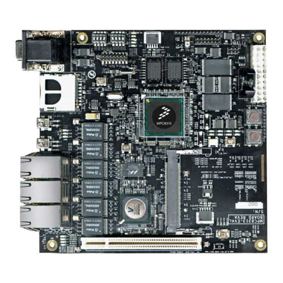
Avoid touching areas of integrated circuitry and connectors; static discharge can damage circuits. WARNING Only the 3.3-V PCI Card is supported. Turn OFF power during insertion and removal of a PCI card. PowerQUICC™ MPC8313E Reference Design Board (RDB), Rev. 4 Freescale Semiconductor... - Page 44 RGMII/ULPI/IEEE1588 selection and L2 Switch/PHY selection Figure 41. MPC8313E-RDB Top View Table 23. Default DIP Switch and Jumper Setting Reference Default Setting 0000 (all ON) 1111 (all OFF) open (no jumper) PowerQUICC™ MPC8313E Reference Design Board (RDB), Rev. 4 Freescale Semiconductor...
- Page 45 RDB. It can be provided by an ATX-type power supply or from a mini-ITX case. WARNING Turn off the main power for the ATX power supply/mini-ITX case before the power connector is attached. PowerQUICC™ MPC8313E Reference Design Board (RDB), Rev. 4 Freescale Semiconductor...
-
Page 46: Mpc8313E Rdb Software
To rebuild the BSP package or to add application software, carefully follow the instructions in . This file contains details on how to build, run, and install the BSP. It guides the Readme.txt PowerQUICC™ MPC8313E Reference Design Board (RDB), Rev. 4 Freescale Semiconductor... -
Page 47: Frequently Asked Questions (Faqs)
• PCI/mini-PCI card can run at 66 MHz (has its M66EN pulled up) and should be used. Even the PCI bus on the RDB runs at only 33 MHz. Otherwise, the PCI frequency is further divided and it becomes 16.6 MHz. PowerQUICC™ MPC8313E Reference Design Board (RDB), Rev. 4 Freescale Semiconductor... - Page 48 Kermit window. success 7. Power off the board and set DIP switch S3 back to ON-ON-ON-ON (0000). 8. Power on the board and you should see a running u-boot. PowerQUICC™ MPC8313E Reference Design Board (RDB), Rev. 4 Freescale Semiconductor...
-
Page 49: Revision History
Number 2/2007 Initial public release. 4/2007 Replaced a faulty table of contents and restructured sections of the document for clarity. 4/2007 Added information to Section 8, Frequently Asked Questions (FAQs) PowerQUICC™ MPC8313E Reference Design Board (RDB), Rev. 4 Freescale Semiconductor... - Page 50 125 MHZ oscillator. • Changed U36 1A linear regulator MIC39100-2.5WS to 3A MIC37302WR for higher 2.5V power consumption by additional PHY. • Changed default DAC to 16-bit SPI controlled MAX5203BEUB+ (U47). PowerQUICC™ MPC8313E Reference Design Board (RDB), Rev. 4 Freescale Semiconductor...
- Page 51 Revision History THIS PAGE INTENTIONALLY LEFT BLANK PowerQUICC™ MPC8313E Reference Design Board (RDB), Rev. 4 Freescale Semiconductor...
- Page 52 Headquarters surgical implant into the body, or other applications intended to support or sustain life, ARCO Tower 15F or for any other application in which the failure of the Freescale Semiconductor product 1-8-1, Shimo-Meguro, Meguro-ku Tokyo 153-0064 could create a situation where personal injury or death may occur. Should Buyer...
Need help?
Do you have a question about the PowerQUICC MPC8313E and is the answer not in the manual?
Questions and answers