
Related Manuals for Freescale Semiconductor MPC5748G


Summary of Contents for Freescale Semiconductor MPC5748G
- Page 1 Freescale Semiconductor, Inc. Document Number: MPC5748GEVBUG User Guide Rev. 0 , 08/2015 MPC5748G EVB User Guide By: Alasdair Robertson © 2015 Freescale Semiconductor, Inc. All rights reserved.
-
Page 2: Table Of Contents
ADC Input Potentiometer (J17, RV1) ............................29 MCU PORT PIN EVB FUNCTIONS ..............................30 DEFAULT JUMPER SUMMARY TABLE ............................31 DEFAULT JUMPER DIAGRAM ............................... 33 REVISION HISTORY ..................................33 APPENDIX ......................................34 MPC5748G EVB User Guide, User Guide, Rev. 0, 08/2015 Freescale Semiconductor, Inc. -
Page 3: Introduction
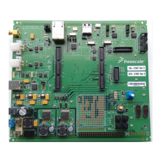
1. Introduction This user guide details the setup and configuration of the Freescale MPC5748G customer Evaluation Board (hereafter referred to as the EVB). The EVB is intended to provide a mechanism for easy evaluation of the MPC5748G family of microcontrollers, and to facilitate hardware and software development. - Page 4 2 mm pitch whereas headers are 0.1 inch (2.54 mm). This prevents inadvertently fitting a jumper to a header. There is no MCU fitted to the EVB. A daughtercard must be fitted before the EVB can be used. MPC5748G EVB User Guide, User Guide, Rev. 0, 08/2015 Freescale Semiconductor, Inc.
-
Page 5: Configuration Overview
The EVB has been designed with ease of use in mind and has been segmented into functional blocks as shown below. Detailed silkscreen legend has been used throughout the board to identify all switches, jumpers and user connectors. Figure 1. EVB Functional Blocks MPC5748G EVB User Guide, User Guide, Rev. 0, 08/2015 Freescale Semiconductor, Inc. -
Page 6: Mcu Daughtercard Information
(viewed from the left side of the EVB). Figure 3. Removing a daughtercard CAUTION Do not attempt to lift the left or right edge of the daughtercard as this will result in connector damage. MPC5748G EVB User Guide, User Guide, Rev. 0, 08/2015 Freescale Semiconductor, Inc. -
Page 7: Initial Configuration
This can be used to connect a bare wire lead to the EVB, typically from a laboratory power supply. The polarisation of the connectors is clearly marked on the EVB. Care must be taken to ensure correct connection. Figure 5. 2-Lever Power Connector MPC5748G EVB User Guide, User Guide, Rev. 0, 08/2015 Freescale Semiconductor, Inc. -
Page 8: Power Switch (Sw5)
EVB and / or components. CAUTION In the event of a short in the regulator output, the regulator and/or the shorted component may be hot MPC5748G EVB User Guide, User Guide, Rev. 0, 08/2015 Freescale Semiconductor, Inc. -
Page 9: Mcu Power Supply Jumpers (J18, J19, J20, J21, J22, J23)
There are an additional two jumpers that control the voltages used by EVB peripherals connected to the VDD_HV_A and VDD_HV_B domains as described in section 5.1.7. Figure 6. Power Supply Jumper Schematic MPC5748G EVB User Guide, User Guide, Rev. 0, 08/2015 Freescale Semiconductor, Inc. -
Page 10: Daughtercard Power Jumpers (J3 To J11)
MCU VDD_HV_C domain is connected to 3.3V (Switching Regulator) 1-2 (D) MCU VDD_HV_C domain is connected to 5.0V (Switching Regulator) Removed MCU VDD_HV_C domain is not connected to power MPC5748G EVB User Guide, User Guide, Rev. 0, 08/2015 Freescale Semiconductor, Inc. -
Page 11: Peripheral Power Supply Jumpers (J24, J25)
In addition, the distribution of the peripheral voltages HVA (J24) and HVB (J25) are shown. Note that jumper J8 (FLA) jumper must only be fitted when VDD_HV_A (J5) is connected to 3.3V. MPC5748G EVB User Guide, User Guide, Rev. 0, 08/2015 Freescale Semiconductor, Inc. - Page 12 USB RS232 (FTDI) transceiver I/O voltage select FlexRay Transceiver I/O Voltage select (and pullups) J25 PER_HVB Nexus Connector reference voltage and Pullups These voltages are fixed due to device specifications and cannot be changed. MPC5748G EVB User Guide, User Guide, Rev. 0, 08/2015 Freescale Semiconductor, Inc.
-
Page 13: Reset Control (J9, Sw1)
5.2.1. Reset LEDs As can be seen in Figure 7 above, there are two reset LED’s that can be used to identify the source / cause of a reset: MPC5748G EVB User Guide, User Guide, Rev. 0, 08/2015 Freescale Semiconductor, Inc. -
Page 14: Mcu Clock Configuration
There are 2 clock configuration jumpers on the daughtercard and an external clock input connector on the main board to allow an externally generated clock to be supplied if desired. See Figure 8 below. Figure 8. EVB Clock Selection MPC5748G EVB User Guide, User Guide, Rev. 0, 08/2015 Freescale Semiconductor, Inc. -
Page 15: External Clock Input (P7)
VDD_HV_A pins. This is selectable between 3.3V and 5.0V on the daughtercard. 5.3.2. MCU Clock Configuration (J1, J2 on Daughtercard) There are two external clock crystals on the MPC5748G daughtercards: 40MHz fast external crystal for clocking the main system clock ... -
Page 16: Debug Connectors (P8, P10)
PER_HVB MSEO_1 PL11 PH10 MDO0 MDO1 JCOMP 10K Pulldown MDO2 MDO3 EVTI EVTO PL12 MCKO PL10 RESET DBUG_RST MDO4 RST_OUT MCU_RST MDO5 CLKOUT Test Point MDO6 PL13 TD/WT MPC5748G EVB User Guide, User Guide, Rev. 0, 08/2015 Freescale Semiconductor, Inc. -
Page 17: Communications & Memory Interfaces
MCU pin if desired. The default configuration is with all jumper headers fitted routing the TX and RX signals to the MCU. MPC5748G EVB User Guide, User Guide, Rev. 0, 08/2015 Freescale Semiconductor, Inc. -
Page 18: Lin Interfaces (P9, P11, J10, J12)
The output from the LIN transceiver is connected to a standard 4-pin Molex connector as used on most other Freescale EVB’s supporting LIN as shown in the following figure: Figure 10. LIN Molex Physical Interface Connector MPC5748G EVB User Guide, User Guide, Rev. 0, 08/2015 Freescale Semiconductor, Inc. -
Page 19: Usb Rs232 Serial Interface (P17, J16)
The MCU LIN2 signals are routed to the FTDI transceiver via a 2-way jumper header (J16) allowing the transceiver to be isolated from the MCU pin if desired. The default configuration is with the jumper MPC5748G EVB User Guide, User Guide, Rev. 0, 08/2015 Freescale Semiconductor, Inc. -
Page 20: Usb Host / Otg Interfaces
The MPC5748G supports both MII and RMII Ethernet interfaces. The EVB incorporates a DP83848c transceiver supporting both MII and RMII modes. The transceiver is connected to a pulse J1011F21PNL RJ45 connector which includes a built-in isolation transformer. - Page 21 If jumper J7 is in position 1-2 (25MHz XTAL), J6 must be fitted and R45 must be fitted. If jumper J7 is in position 2-3 (50MHz oscillator), J6 must be removed and R45 must be removed and placed between R45 and R80 MPC5748G EVB User Guide, User Guide, Rev. 0, 08/2015 Freescale Semiconductor, Inc.
-
Page 22: Flexray (P2, P3, J1, J2, J3, J4)
FlexRay B PHY will enter Standby Mode Removed FITTED (D) FlexRay B PHY Wakeup signal pulled low WAKE Posn 7-8 FlexRay B PHY Wakeup signal pulled high Removed MPC5748G EVB User Guide, User Guide, Rev. 0, 08/2015 Freescale Semiconductor, Inc. -
Page 23: Sd Card Socket (P200)
The EVB supports a 4-bit SD interface (note that MPC5748G supports 8-bit SD data) which is routed to a full sized SD card connector on the underside of the EVB. There is no user configuration required. - Page 24 Note that connector P25 is not populated and must be fitted if required CAUTION Before the daughtercard is installed or removed, the EVB must be powered OFF to prevent potential damage to the EVB or daughter card components. MPC5748G EVB User Guide, User Guide, Rev. 0, 08/2015 Freescale Semiconductor, Inc.
-
Page 25: Twrpi Connectors (P26, P27)
As with all daughtercards, the EVB must be powered OFF to prevent damage to the EVB or daughter card components. ID0 and ID1 have a 10K pullup to 3V3 MPC5748G EVB User Guide, User Guide, Rev. 0, 08/2015 Freescale Semiconductor, Inc. -
Page 26: User Interface (I/O)
In addition there are GPIO pins that are shared with the SAI Audio and TWRPI connectors as detailed below and shaded orange. These are totally available unless the SAI / TWRPI headers are being used. PA[12..15], PD[4..8], PG[2..5], PK[0..4], PO[0..1] MPC5748G EVB User Guide, User Guide, Rev. 0, 08/2015 Freescale Semiconductor, Inc. -
Page 27: User Switches (Sw3, Sw4, Sw6, Sw7, P22)
MCU pins. These can be removed if required to isolate the switch from the respective MCU pin (useful if the switch is being manually routed to another pin on the GPIO matrix). MPC5748G EVB User Guide, User Guide, Rev. 0, 08/2015 Freescale Semiconductor, Inc. -
Page 28: Hex Encoder Switch (Sw2, J26, P20)
MCU pins. These can be removed if required to isolate the switch from the respective MCU pin (useful if the switch is being manually routed to another pin on the GPIO matrix). MPC5748G EVB User Guide, User Guide, Rev. 0, 08/2015 Freescale Semiconductor, Inc. -
Page 29: User Led's (Ds2, Ds3, Ds7, Ds8, P19)
Output from RV1 is routed to MCU PB4 pin FITTED (D) MCU PB4 is not connected to RV1 Removed There is also a test point TP18 connected to the variable resistor output for monitoring purposes. MPC5748G EVB User Guide, User Guide, Rev. 0, 08/2015 Freescale Semiconductor, Inc. -
Page 30: Mcu Port Pin Evb Functions
Shared with MLB header (via no populated zero ohm resistors) Shared with user switches Shared with Hex Encoder Switch Shared with user LED’s Shared with TWRPI (P26, P27) or SAI Audio P25 MPC5748G EVB User Guide, User Guide, Rev. 0, 08/2015 Freescale Semiconductor, Inc. -
Page 31: Default Jumper Summary Table
EVB peripherals in HVB domain are set to use I/O voltage of 3.3V J25 (HVB) J26 (3V3) Fitted (D) The hex encoder switch is powered with 3.3V (functional) MPC5748G EVB User Guide, User Guide, Rev. 0, 08/2015 Freescale Semiconductor, Inc. - Page 32 Ballast collector supply is enabled (jumper can be used for current measure) ** Only valid on certain devices – External Ballast enabled. 1-2 (D) Note that not all jumpers will be present on all of the daughtercards. MPC5748G EVB User Guide, User Guide, Rev. 0, 08/2015 Freescale Semiconductor, Inc.
-
Page 33: Default Jumper Diagram
Following figure is of an older board revision however there were no additional jumpers and no jumpers have moved position. Figure 13. Default Jumper Position 12. Revision History Date Substantial changes August 2015 Initial release MPC5748G EVB User Guide, User Guide, Rev. 0, 08/2015 Freescale Semiconductor, Inc. -
Page 34: Appendix
The following EVB schematics are detailed in the following sections: Main EVB (motherboards) 324BGA Daughtercard 256BGA Daughtercard 176QFP Daughtercard 100QFP Daughtercard (MPC5746C only) MPC5748G EVB User Guide, User Guide, Rev. 0, 08/2015 Freescale Semiconductor, Inc. - Page 35 Main EVB...
- Page 36 MPC574xx Customer Evaluation Board (X-MPC574XG-MB) Revision Information Rev Date Designer Comments Table Of Contents: 01 Feb 2012 Alasdair Robertson Start of capture, Working version Power - Main input and Linear voltage regulators Sheet 2 19 Feb 2012 Alasdair Robertson 1st release for internal review (Complete Board) Power - Switching voltage regulators Sheet 3 28 Feb 2012...
- Page 37 Power Input and Linear Voltage Regulators Input 12V DC nominal (range 10v - 14v) See note on schematic sheet 3 regarding 3.3V regulator when running at < 11V) Power Supply Input and Filter Test and reference points (Power Switch) GND11 GND13 GND1 GND2...
- Page 38 Switching Voltage Regulators and Supply Jumpers Global MCU Daughtercard To Daughtercard 5.0v Switching Regulator Supply Jumpers and DC power Connectors Vout = 1.21(1 + Rfb2/Rfb1) = 4.98V (All Resistors 1% 0603_CC) P12V Rfb1 R295 R294 1.0K DC_P12V R268 DC_P12V 5V0_SR R296 1.47K R298 1.65K Rfb2...
- Page 39 Daughter Card Connectors (Sockets) Notes: - there was no neat way to fit these connectors onto a B sized sheet so unfortunately the sheet size has been increased to C so will need to be printed on larger paper. - The MCU Clock circuitry (apart from external clock) is local to the daughtercard so not pinned out on the connectors - Power is supplied to the daughtercard via MCU specific jumpered supplies (left connector) or direct supplies from the regulators (right connector)
- Page 40 0.1UF 50V) R214 Note: The Reset pad on the MPC5748G is in the VDD_HV_A domain which can be run from either LED RED 3.3V or 5V (selected by the VDD_HV_A and PER_HVA jumpers) (MCU RESET) To maintian brightness on the LED's irrespective of the voltage setting, the LED's are powered from constant 3.3V, grounded via the reset line.
- Page 41 Debug Connectors (JTAG and NEXUS) JTAG Standard 14-pin Connector (All JTAG reset pullups are on Reset Page) Voltage Domains: PER_HVA All of the signals used for JTAG (with the exception of EVTI, see note) are powered from Note on EVTI: the VDD_HV_A domain.
- Page 42 CAN & LIN Physical CAN0 Physical Interface 5V0_SR PER_HVA - 5.0V input supply for CAN transceiver (4.5 to 5.5V) C255 C254 VI/O - determines the signal level on MCU TX and RX pins C270 C271 0.1UF 0.1UF and can range from 2.8 to 5.5V (0603 (0603 STB - High for Standby mode, pulled low for normal mode.
- Page 43 USB RS232 (serial) Interface All Signals are in FTDI USB <-> Serial Interface power domain VDD_HV_A. - Self Powered mode. No power is taken from USB - Device efaults to Dual serial (RS232) mode ie RS232 on both A and B FTDI interface will - Configurable I/O voltage on CHA / CHB via VDDIOA/B 5V0_SR...
- Page 44 USB (Type A Host and Type AB OTG) 3V3_SR 5V0_SR USB Signals General Layout Note. Recommendation is to keep all are in tracks between MCU and USB PHI less than 3" See Adobe Acrobat power Document domain C239 C236 C230 additional SMSC Layout guidelines PDF to the right C243 10UF...
- Page 45 Ethernet All Ethernet Signals are in power domain 50MHz Osc for RMII and 25MHz XTAL for MII 3V3_SR 3V3_SR L200 VDD_HV_B C200 (0603 120OHM 0.1UF RMII_50MHZ 50V) The Ethernet Layout Note - Place Caps and Resistors close to PHI interface only C227 C232 C223...
- Page 46 FlexRAY Physical Interface All Signals are in Decoupling Caps for BOTH IC's. Place next to power pins. power domain VDD_HV_A. PER_HVA P12V 5V0_SR FlexRAY interface will FlexRAY debug work at 3.3V or 5.0V connector (PER_HVA jumper) PC12 (FR_DBG0) (FR_DBG1) PC12 C209 C221 C222...
- Page 47 SAI Audio, AVB & TWRPI Connectors General Purpose TWRPI 3V3_SR 5V0_SR 3V3_SR 3V3_LR 3V3_SR 3V3_SR 3V3_SR R316 R315 10.0K R317 10.0K R318 10.0K 10.0K R314 I2C0_SCL I2C0_SDA 4,16 TWRPI-ADC0 TWRPI-ADC1 PA12 (DSPI0_SIN) (DSPI0_SOUT) PA13 4,16 (ADC1_P[10]) TWRPI-ADC2 PA15 (DSPI0_SS0) (DSPI0_SCK) PA14 (EIRQ31) (GPIO0/IRQ)
- Page 48 MLB (SMSC) Daughtercard Connector 3V3_SR Layout Note: MLB track lengths should be < 80mm (from MCU through daughter card to connector) 3V3_LR P12V All MLB Signals are in (12v) (3.3v) 10.0K 10.0K 10.0K power domain VDD_HV_C. (3.3v Linear) (3.3v) (RSVD) (SDA) (I2C1_SDA) CARD INTERRUPTING MCU (WKPU21)
- Page 49 SD Connector Caution The SD card specification details an operating voltage of between 2.7 and 3.6V. If using the SD card, it can ONLY be used when VDD_HV_A (and PER_HVA) jumpers are set to 3.3V. 3V3_SR Inserting an SD card with VDD_HV_A / PER_HVA set to 5V will result in card damage.
- Page 50 User Peripherals, Audio Controls and GPIO Switches are hard wired to 3.3V rather than 5V so it's not possible to drive 5V into a 3.3V pad (which would cause damage) Similarly, the LED's are active low with 3.3v supply so can be safely coupled to pads on either 3.3V or 5V domains The ADC input is limited to 3.3V, again to prevent driving 5V into a 3.3V pad which would cause damage User LED's (Active Low) ADC Input Pot and Test Point...
- Page 51 GPIO Pin Matrix All pads are DNP (Do Not Populate) 0.1" pitch headers placed on a 0.1" grid 4,15 PF10 PF[9,11] shared with PORTA PORTB PORTC PORTD PORTE PORTF PORTG PORTH PF10 PF11 user switches PF11 4,15 PF12 PF12 PF13 4,15 PF13 PA[1,2] shared with...
- Page 52 324 BGA DC...
- Page 53 Freescale does not make any warranty, implied or otherwise, as to the suitability of circuit design or component selection (type or value) used in these schematics for hardware design using the Freescale MPC5748G family 3 Different test points used in design: of Microprocessors.
- Page 54 Freescale General Business Use Freescale General Business Use Freescale General Business Use Drawing Title: Drawing Title: Drawing Title: MPC5748G 324 BGA Daughter Card MPC5748G 324 BGA Daughter Card MPC5748G 324 BGA Daughter Card Ground Links Page Title: Page Title: Page Title:...
- Page 55 MPC5748G MCU Decoupling and bulk storage Capacitor Types: Flash 470pF - Ceramic COG, 50v 5% 0402 1000pF - Ceramic COG, 50V 5% 0402 ADC0_CAP ADC1_CAP ADC1REF_CAP HVFLA_CAP 4700pF - Ceramic X7R, 50V 10% 0402 1000pF 1000pF 0.01uF - Ceramic X7R, 50V 10% 0402 0.1uF...
- Page 56 MPC5748G GPIO 1 of 2 (SD_CD - WKPU19) (MLB_I2C1_SCL) ** PA1 is also NMI. Routed (WKPU2 / NMI0) (SW1 & GPIO**) (MLB_I2C1_SDA) MPC5748G 324 BGA to I/O Matrix (WKPU3) (SW2 & GPIO) (FR_A_TX_EN) (MII_RXCLK) (FR_A_RX) (CMP1_13 / IO) (FR_B_TX) Package 1of3 GPIO Pins1...
- Page 57 MPC5748G GPIO 2 of 2 Key to text colours: Purple - Comms Physical Interfaces Orange - Other Peripherals and I/O (SD_D3) (MDO9) Blue - Debug (JTAG & Nexus) (SD_D2) (MDO10) MPC5748G 324 BGA Black - Clock, Reset and Control (SD_D1)
- Page 58 Freescale General Business Use Freescale General Business Use Freescale General Business Use Drawing Title: Drawing Title: Drawing Title: MPC5748G 324 BGA Daughter Card MPC5748G 324 BGA Daughter Card MPC5748G 324 BGA Daughter Card Page Title: Page Title: Page Title: Clocks...
- Page 59 Freescale General Business Use Freescale General Business Use Freescale General Business Use Drawing Title: Drawing Title: Drawing Title: MPC5748G 324 BGA Daughter Card MPC5748G 324 BGA Daughter Card MPC5748G 324 BGA Daughter Card Page Title: Page Title: Page Title: High Speed Signal Termination...
- Page 60 Freescale General Business Use Freescale General Business Use Freescale General Business Use Drawing Title: Drawing Title: Drawing Title: MPC5748G 324 BGA Daughter Card MPC5748G 324 BGA Daughter Card MPC5748G 324 BGA Daughter Card Page Title: Page Title: Page Title: Daughter Card Connectors (Plugs)
- Page 61 256 BGA DC...
- Page 62 Freescale does not make any warranty, implied or otherwise, as to the suitability of circuit design or component selection (type or value) used in these schematics for hardware design using the Freescale MPC5748G family of Microprocessors. Customers using any part of these schematics as a basis for hardware design, do so at their own risk and Freescale does not assume any liability for such a hardware design.
- Page 63 Freescale General Business Use Freescale General Business Use Freescale General Business Use TPH1 Drawing Title: Drawing Title: Drawing Title: MPC5748G 256 BGA Daughter Card MPC5748G 256 BGA Daughter Card MPC5748G 256 BGA Daughter Card Ground Links Page Title: Page Title: Page Title: (0 Ohm 1.0 UF...
- Page 64 MPC5748G MCU Decoupling and bulk storage Capacitor Types: Flash 470pF - Ceramic COG, 50v 5% 0402 1000pF - Ceramic COG, 50V 5% 0402 ADC0_CAP ADC1_CAP ADC1REF_CAP HVFLA_CAP 4700pF - Ceramic X7R, 50V 10% 0402 1000pF 1000pF 0.01uF - Ceramic X7R, 50V 10% 0402 0.1uF...
- Page 65 MPC5748G GPIO 1 of 2 (SD_CD - WKPU19) (MLB_I2C1_SCL) (WKPU2 / NMI0) (SW1 & GPIO**) (MLB_I2C1_SDA) MPC5748G 256 BGA ** PA1 is also NMI. Routed to I/O Matrix (WKPU3) (SW2 & GPIO) (FR_A_TX_EN) (MII_RXCLK) (FR_A_RX) (CMP1_13 / IO) (FR_B_TX) Package 1of3 GPIO Pins1...
- Page 66 MPC5748G GPIO 2 of 2 Key to text colours: (SD_D3) Purple - Comms Physical Interfaces (SD_D2) MPC5748G 256 BGA Orange - Other Peripherals and I/O (SD_D1) Blue - Debug (JTAG & Nexus) (SD_D0) (GPIO) Black - Clock, Reset and Control...
- Page 67 Freescale General Business Use Freescale General Business Use Freescale General Business Use Drawing Title: Drawing Title: Drawing Title: MPC5748G 256 BGA Daughter Card MPC5748G 256 BGA Daughter Card MPC5748G 256 BGA Daughter Card Page Title: Page Title: Page Title: Clocks...
- Page 68 Freescale General Business Use Freescale General Business Use Freescale General Business Use Drawing Title: Drawing Title: Drawing Title: MPC5748G 256 BGA Daughter Card MPC5748G 256 BGA Daughter Card MPC5748G 256 BGA Daughter Card Page Title: Page Title: Page Title: High Speed Signal Termination...
- Page 69 Freescale General Business Use Freescale General Business Use Freescale General Business Use Drawing Title: Drawing Title: Drawing Title: MPC5748G 256 BGA Daughter Card MPC5748G 256 BGA Daughter Card MPC5748G 256 BGA Daughter Card Page Title: Page Title: Page Title: Daughter Card Connectors (Plugs)
- Page 70 176 QFP DC...
- Page 71 Freescale does not make any warranty, implied or otherwise, as to the suitability of circuit design or component selection (type or value) used in these schematics for hardware design using the Freescale MPC5748G family of Microprocessors. Customers using any part of these schematics as a basis for hardware design, do so at their own risk and Freescale does not assume any liability for such a hardware design.
- Page 72 Freescale General Business Use Freescale General Business Use MPC5746 Drawing Title: Drawing Title: Drawing Title: INT_BAL_SELECT enable MPC5748G 176 QFP Daughter Card MPC5748G 176 QFP Daughter Card MPC5748G 176 QFP Daughter Card Ground Links Page Title: Page Title: Page Title: (0 Ohm 1.0 UF...
- Page 73 MPC5748G MCU Decoupling and bulk storage Capacitor Types: Flash 470pF - Ceramic COG, 50v 5% 0402 1000pF - Ceramic COG, 50V 5% 0402 ADC0_CAP ADC1_CAP ADC1REF_CAP HVFLA_CAP 4700pF - Ceramic X7R, 50V 10% 0402 1000pF 1000pF 0.01uF - Ceramic X7R, 50V 10% 0402 0.1uF...
- Page 74 MPC5748G GPIO 1 of 2 (SD_CD - WKPU19) (MLB_I2C1_SCL) (WKPU2 / NMI0) (SW1 & GPIO**) (MLB_I2C1_SDA) MPC5748G 176QFP ** PA1 is also NMI. Routed to I/O Matrix (WKPU3) (SW2 & GPIO) (FR_A_TX_EN) (MII_RXCLK) (FR_A_RX) (CMP1_13 / IO) (FR_B_TX) Package 1of3 GPIO Pins1...
- Page 75 MPC5748G GPIO 2 of 2 Key to text colours: (SD_D3) Purple - Comms Physical Interfaces (SD_D2) MPC5748G 176QFP Orange - Other Peripherals and I/O (SD_D1) Blue - Debug (JTAG & Nexus) (SD_D0) Black - Clock, Reset and Control (USB1_STP) Package 3of3 GPIO Pins2...
- Page 76 Freescale General Business Use Freescale General Business Use Freescale General Business Use Drawing Title: Drawing Title: Drawing Title: MPC5748G 176 QFP Daughter Card MPC5748G 176 QFP Daughter Card MPC5748G 176 QFP Daughter Card Page Title: Page Title: Page Title: Clocks...
- Page 77 Freescale General Business Use Freescale General Business Use Freescale General Business Use Drawing Title: Drawing Title: Drawing Title: MPC5748G 176 QFP Daughter Card MPC5748G 176 QFP Daughter Card MPC5748G 176 QFP Daughter Card Page Title: Page Title: Page Title: High Speed Signal Termination...
- Page 78 Freescale General Business Use Freescale General Business Use Freescale General Business Use Drawing Title: Drawing Title: Drawing Title: MPC5748G 176 QFP Daughter Card MPC5748G 176 QFP Daughter Card MPC5748G 176 QFP Daughter Card Page Title: Page Title: Page Title: Daughter Card Connectors (Plugs)
- Page 79 100 QFP DC...
- Page 80 MPC5746C Customer EVB 100 BGA Daughter Card (MPC574XG-100DS) Revision Information Rev Date Designer Comments Table Of Contents: 05 Jan 2014 Alasdair Robertson Initial release sent for review based on X-MPC574XG-256DS RevA Power - MPC5746C power pins footprint Sheet 2 07 Jan 2014 Alasdair Robertson Post review corrections incl MCU Orcad Footprint Power - MPC5746C Decoupling Capacitors...
- Page 81 MPC5746C MCU Power Connections Caution: Default Configuraiton: - ALL MCU supply voltages are set to 3.3V (ADC0, ADC1, VDD_HV_A, - If VDD_HV_A is driven from 5V, the VDD_HV_FLA pin VDD_HV_B, VDD_HV_C, VBallast) must not be supplied from 3.3V (remove the HVA_FLA - VDD_HV_FLA = External 3.3V supplied (jumper fitted) jumper) - VDD_LV Supplied from ballast transistor...
- Page 82 MPC5746C MCU Decoupling and bulk storage Capacitor Types: Flash 470pF - Ceramic COG, 50v 5% 0402 1000pF - Ceramic COG, 50V 5% 0402 ADC0_CAP ADC1_CAP ADC1REF_CAP HVFLA_CAP 4700pF - Ceramic X7R, 50V 10% 0402 1000pF 1000pF 0.01uF - Ceramic X7R, 50V 10% 0402 0.1uF - Ceramic X7R, 16V 10%...
- Page 83 MPC5746C GPIO 1 of 2 (SD_CD - WKPU19) (WKPU2 / NMI0) (SW1 & GPIO**) MPC5746C 100 BGA ** PA1 is also NMI. Routed to I/O Matrix (WKPU3) (SW2 & GPIO) (FR_A_TX_EN) (MII_RXCLK) (FR_A_RX) (CMP1_13 / IO) Package 1of3 GPIO Pins1 Key to text colours: (SAI_GPIO) Purple...
- Page 84 MPC5746C GPIO 2 of 2 Key to text colours: (SD_D3) Purple - Comms Physical Interfaces (SD_D2) MPC5746C 100 BGA Orange - Other Peripherals and I/O (SD_D1) Blue - Debug (JTAG & Nexus) (SD_D0) Black - Clock, Reset and Control Package 3of3 GPIO Pins2 - I/O Matrix and other functions (eg LED) Green - I/O Matrix (dedicated)
- Page 85 Clocks Oscillators and External Clock EXT-CLK (From SMA connector on main board) EXT-CLK (Note the 32KHz osc pins are not bonded 12PF out on the 100 pin EXTAL package) 1.0M 40.0MHZ MCU-EXTAL 12PF MCU-EXTAL XTAL MCU-XTAL MCU-XTAL NX8045GB-40.000M-STD-CSJ-1 XTAL (Optimised for Automotive, 8pF Load capacitance) Automotive Microcontroller Automotive Microcontroller Automotive Microcontroller...
- Page 86 High Speed Signal Termination Ethernet Termination PG13 PG13-R PG13 PG13-R PG12 PG12-R PG12 PG12-R PH0-R PH0-R PH1-R PH1-R PH2-R PH2-R PG0-R PG0-R Place resistors as close as possible to MCU Automotive Microcontroller Automotive Microcontroller Automotive Microcontroller Applications Applications Applications East Kilbride, Scotland East Kilbride, Scotland East Kilbride, Scotland Freescale General Business Use...
- Page 87 Daughter Card Connectors (Plugs) Notes: Connectors on Main board (Shown for reference) - there was no neat way to fit these connectors onto a B sized sheet so unfortunately the sheet size has been increased to C so will need to be printed on larger paper. - The Crystal Signals are NOT routed via the daughtercard connectors - The Specific MCU power pins are not routed via the daughter card however the jumpered MCU supply lines are brought up from the main board (see the top pins of the connector on the left)
- Page 88 Freescale sells products pursuant to standard terms and conditions of sale, which can be found at the following address: freescale.com/SalesTermsandConditions. Freescale and the Freescale logo are trademarks of Freescale Semiconductor, Inc., Reg. U.S. Pat. & Tm. Off. All other product or service names are the property of their respective owners.
Need help?
Do you have a question about the MPC5748G and is the answer not in the manual?
Questions and answers