
Related Manuals for Intel BX80571E5300 - Pentium 2.6 GHz Processor


Summary of Contents for Intel BX80571E5300 - Pentium 2.6 GHz Processor
- Page 1 ® ® Intel Pentium Dual-Core Δ Processor E5000 Series Datasheet December 2008 Document Number: 320467-002...
- Page 2 Contact your local Intel sales office or your distributor to obtain the latest specifications and before placing your product order. Intel, Pentium, Intel Core, Intel SpeedStep, and the Intel logo are trademarks of Intel Corporation in the U.S. and other countries.
-
Page 3: Table Of Contents
Contents Introduction ....................9 Terminology ....................... 9 1.1.1 Processor Terminology Definitions ............10 References ....................... 11 Electrical Specifications ................13 Power and Ground Lands..................13 Decoupling Guidelines ..................13 2.2.1 VCC Decoupling ..................13 2.2.2 VTT Decoupling ..................13 2.2.3 FSB Decoupling.................. - Page 4 Sleep State ....................88 6.2.6 Deep Sleep State..................89 6.2.7 Deeper Sleep State .................89 ® 6.2.8 Enhanced Intel SpeedStep Technology ............90 Processor Power Status Indicator (PSI) Signal ............90 Boxed Processor Specifications ................ 91 Introduction ......................91 Mechanical Specifications ..................92 7.2.1 Boxed Processor Cooling Solution Dimensions..........92 7.2.2...
- Page 5 Figures Processor V Static and Transient Tolerance............... 20 Overshoot Example Waveform ................21 Differential Clock Waveform ..................30 Measurement Points for Differential Clock Waveforms ........... 31 Processor Package Assembly Sketch ................33 Processor Package Drawing Sheet 1 of 3 ..............34 Processor Package Drawing Sheet 2 of 3 ..............
- Page 6 Tables References ......................11 Voltage Identification Definition ..................15 Absolute Maximum and Minimum Ratings ..............17 Voltage and Current Specifications................18 Processor V Static and Transient Tolerance ...............19 Overshoot Specifications..................20 FSB Signal Groups ....................22 Signal Characteristics....................23 Signal Reference Voltages ..................23 GTL+ Signal Group DC Specifications ................24 Open Drain and TAP Output Signal Group DC Specifications ...........24 CMOS Signal Group DC Specifications................25 PECI DC Electrical Limits ...................26...
- Page 7 Intel architecture enables the processor to execute operating systems and applications written ® to take advantage of the Intel 64 architecture. The processor, supporting Enhanced Intel Speedstep technology, allows tradeoffs to be made between performance and power consumption. ® The Intel Pentium dual-core processor E5000 series also includes the Execute Disable Bit capability.
-
Page 8: Revision History
Revision History Revision Description Revision Date Number • Initial release August 2008 -001 ® ® • Intel Pentium dual-core processor E5300 December 2008 -002 § § Datasheet... -
Page 9: Introduction
LGA775 socket. ® The processor is based on 45 nm process technology. The processors feature the Intel Advanced Smart Cache, a shared multi-core optimized cache that significantly reduces latency to frequently used data. The processor features an 800 MHz front side bus (FSB) and 2 MB of L2 cache. -
Page 10: Processor Terminology Definitions
64 Architecture— An enhancement to Intel's IA-32 architecture, allowing the processor to execute operating systems and applications written to take advantage of the Intel 64 architecture. Further details on Intel 64 architecture and programming model can be found in the Intel Extended Memory 64 Technology... -
Page 11: References
Intel Pentium Dual-Core Processor E5000 Series Specification design/processor/ Update specupdt/320467.pdf ® ® Intel Core™2 Duo processor E8000 and E7000 Series, and Intel www.intel.com/design/ ® Pentium Dual-Core Processor E5000 Series Thermal and processor/designex/ Mechanical Design Guidelines 318734.htm http://www.intel.com/ Voltage Regulator-Down (VRD) 11.0 Processor Power Delivery... - Page 12 Introduction Datasheet...
-
Page 13: Electrical Specifications
In addition, ceramic decoupling capacitors are required to filter high frequency content generated by the front side bus and processor activity. Consult the Voltage Regulator-Down (VRD) 11.0 Processor Power Delivery Design Guidelines For Desktop LGA775 Socket for further information. Contact your Intel field representative for additional information. 2.2.2 Decoupling Decoupling must be provided on the motherboard. -
Page 14: Fsb Decoupling
® reflected by the VID Range values provided in Table 4. Refer to the Intel Pentium dual-core Processor E5000 Series Specification Update for further details on specific valid core frequency and VID values of the processor. Note that this differs from the VID employed by the processor during a power management event (Thermal Monitor 2, ®... -
Page 15: Voltage Identification Definition
Electrical Specifications Table 2. Voltage Identification Definition Voltage Voltage 1.0375 1.025 1.5875 1.0125 1.575 1.5625 0.9875 1.55 0.975 1.5375 0.9625 1.525 0.95 1.5125 0.9375 0.925 1.4875 0.9125 1.475 1.4625 0.8875 1.45 0.875 1.4375 0.8625 1.425 0.85 1.4125 0.8375 0.825 1.3875 0.8125 1.375 1.3625... -
Page 16: Reserved, Unused, And Testhi Signals
Electrical Specifications Reserved, Unused, and TESTHI Signals All RESERVED lands must remain unconnected. Connection of these lands to V or to any other signal (including each other) can result in component malfunction or incompatibility with future processors. See Chapter 4 for a land listing of the processor and the location of all RESERVED lands. -
Page 17: Voltage And Current Specification
Electrical Specifications Voltage and Current Specification 2.6.1 Absolute Maximum and Minimum Ratings Table 3 specifies absolute maximum and minimum ratings only and lie outside the functional limits of the processor. Within functional operation limits, functionality and long-term reliability can be expected. At conditions outside functional operation condition limits, but within absolute maximum and minimum ratings, neither functionality nor long-term reliability can be expected. -
Page 18: Dc Voltage And Current Specification
VID range. Note that this differs from the VID employed by the processor during a power management event (Thermal Monitor 2, Enhanced Intel ®... - Page 19 Electrical Specifications must be provided via a separate voltage source and not be connected to V . This specification is measured at the land. Baseboard bandwidth is limited to 20 MHz. This is the maximum total current drawn from the V plane by only the processor.
-
Page 20: Vcc Overshoot
Electrical Specifications Figure 1. Processor V Static and Transient Tolerance Icc [A] VID - 0.000 VID - 0.013 VID - 0.025 Vcc Maximum VID - 0.038 VID - 0.050 VID - 0.063 VID - 0.075 Vcc Typical VID - 0.088 VID - 0.100 VID - 0.113 Vcc Minimum... -
Page 21: Die Voltage Validation
GTLREF specifications). Termination resistors (R ) for GTL+ signals are provided on the processor silicon and are terminated to V . Intel chipsets will also provide on-die termination, thus eliminating the need to terminate the bus on the motherboard for most GTL+ signals. -
Page 22: Fsb Signal Groups
Electrical Specifications 2.7.1 FSB Signal Groups The front side bus signals have been combined into groups by buffer type. GTL+ input signals have differential input buffers, which use GTLREF[1:0] as a reference level. In this document, the term “GTL+ Input” refers to the GTL+ input group as well as the GTL+ I/O group when receiving. -
Page 23: Cmos And Open Drain Signals
Electrical Specifications The value of these signals during the active-to-inactive edge of RESET# defines the processor configuration options. See Section 6.1 for details. PROCHOT# signal type is open drain output and CMOS input. Table 8. Signal Characteristics Signals with R Signals with No R A20M#, BCLK[1:0], BPM[5:0]#, BSEL[2:0], A[35:3]#, ADS#, ADSTB[1:0]#, BNR#, BPRI#,... -
Page 24: Processor Dc Specifications
Electrical Specifications 2.7.3 Processor DC Specifications The processor DC specifications in this section are defined at the processor core (pads) unless otherwise stated. All specifications apply to all frequencies and cache sizes unless otherwise stated. Table 10. GTL+ Signal Group DC Specifications Symbol Parameter Unit... -
Page 25: Platform Environment Control Interface (Peci) Dc Specifications
2.7.3.1 Platform Environment Control Interface (PECI) DC Specifications PECI is an Intel proprietary one-wire interface that provides a communication channel between Intel processors, chipsets, and external thermal monitoring devices. The processor contains Digital Thermal Sensors (DTS) distributed throughout die. These... -
Page 26: Gtl+ Front Side Bus Specifications
Electrical Specifications Table 13. PECI DC Electrical Limits Symbol Definition and Conditions Units Notes Input Voltage Range -0.15 Hysteresis 0.1 * V — hysteresis Negative-edge threshold voltage 0.275 * V 0.500 * V Positive-edge threshold voltage 0.550 * V 0.725 * V High level output source -6.0 source... -
Page 27: Clock Specifications
The processor supports Half Ratios between 7.5 and 13.5, refer to Table 15 for the processor supported ratios. The processor uses a differential clocking implementation. For more information on the processor clocking, contact your Intel field representative. Datasheet... -
Page 28: Fsb Frequency Select Signals (Bsel[2:0])
Electrical Specifications Table 15. Core Frequency to FSB Multiplier Configuration Multiplication of System Core Core Frequency 1, 2 Notes Frequency to FSB Frequency (200 MHz BCLK/800 MHz FSB) 1.20 GHz 1.40 GHz 1.5 GHz 1/7.5 1.60 GHz 1/8.5 1.70 GHz 1.80 GHz 1.90 GHz 1/9.5... -
Page 29: Phase Lock Loop (Pll) And Filter
Electrical Specifications Table 16. BSEL[2:0] Frequency Table for BCLK[1:0] BSEL2 BSEL1 BSEL0 FSB Frequency Rerserved Rerserved Rerserved 200 MHz Rerserved Rerserved Rerserved Rerserved 2.8.3 Phase Lock Loop (PLL) and Filter An on-die PLL filter solution will be implemented on the processor. The VCCPLL input is used for the PLL. -
Page 30: Differential Clock Waveform
Electrical Specifications Table 18. FSB Differential Clock Specifications (800 MHz FSB) T# Parameter Unit Figure Notes 198.980 — 200.020 BCLK[1:0] Frequency 4.99950 — 5.00050 T1: BCLK[1:0] Period — — T2: BCLK[1:0] Period Stability — V/nS T5: BCLK[1:0] Rise and Fall Slew Rate T6: Slew Rate Matching NOTES: Unless otherwise noted, all specifications in this table apply to all processor core frequencies... -
Page 31: Measurement Points For Differential Clock Waveforms
Electrical Specifications Figure 4. Measurement Points for Differential Clock Waveforms Slew_rise Slew _fall +150 mV +150mV 0.0V V_swing 0.0V -150 mV -150mV Diff T5 = BCLK[1:0] rise and fall time through the swing region § § Datasheet... - Page 32 Electrical Specifications Datasheet...
-
Page 33: Package Mechanical Specifications
Package Mechanical Specifications Package Mechanical Specifications The processor is packaged in a Flip-Chip Land Grid Array (FC-LGA8) package that interfaces with the motherboard via an LGA775 socket. The package consists of a processor core mounted on a substrate land-carrier. An integrated heat spreader (IHS) is attached to the package substrate and core and serves as the mating surface for processor component thermal solutions, such as a heatsink. -
Page 34: Processor Package Drawing Sheet 1 Of 3
Package Mechanical Specifications Figure 6. Processor Package Drawing Sheet 1 of 3 Datasheet... -
Page 35: Processor Package Drawing Sheet 2 Of 3
Package Mechanical Specifications Figure 7. Processor Package Drawing Sheet 2 of 3 Datasheet... -
Page 36: Processor Package Drawing Sheet 3 Of 3
Package Mechanical Specifications Figure 8. Processor Package Drawing Sheet 3 of 3 Datasheet... -
Page 37: Processor Component Keep-Out Zones
Package Mechanical Specifications Processor Component Keep-Out Zones The processor may contain components on the substrate that define component keep- out zone requirements. A thermal and mechanical solution design must not intrude into the required keep-out zones. Decoupling capacitors are typically mounted to either the topside or land-side of the package substrate. -
Page 38: Package Insertion Specifications
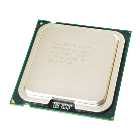
Processor Markings Figure 9 shows the topside markings on the processor. This diagram is to aid in the identification of the processor. Figure 9. Processor Top-Side Markings Example INTEL ©'06 E5200 Intel® Pentium® Dual-Core SLAY7 [COO] 2.50GHZ/2M/800/06 [FPO] ATPO Datasheet... -
Page 39: Processor Land Coordinates
Package Mechanical Specifications Processor Land Coordinates Figure 10 shows the top view of the processor land coordinates. The coordinates are referred to throughout the document to identify processor lands. Figure 10. Processor Land Coordinates and Quadrants, Top View Address/ Socket 775 Common Clock/ Quadrants Async... - Page 40 Package Mechanical Specifications Datasheet...
-
Page 41: Land Listing And Signal Descriptions
Land Listing and Signal Descriptions Land Listing and Signal Descriptions This chapter provides the processor land assignment and signal descriptions. Processor Land Assignments This section contains the land listings for the processor. The land-out footprint is shown Figure 11 Figure 12. -
Page 42: Land-Out Diagram (Top View - Left Side)
Land Listing and Signal Descriptions Figure 11. land-out Diagram (Top View – Left Side) FC34 FC31 BSEL1 FC15 FC33 FC32 BSEL2 BSEL0 BCLK1 TESTHI4 TESTHI5 TESTHI3 TESTHI6 RESET# D47# D44# DSTBN2# DSTBP2# D35# D36# D32# D31# RSVD BCLK0 VTT_SEL TESTHI0 TESTHI2 TESTHI7 RSVD D43# D41#... -
Page 43: Land-Out Diagram (Top View - Right Side)
Land Listing and Signal Descriptions Figure 12. land-out Diagram (Top View – Right Side) VID_SEL VSS_MB_RE VCC_MB_ VSS_ VCC_ GULATION REGULATION SENSE SENSE VID7 FC40 VID6 VID2 VID0 VID3 VID1 VID5 VRDSEL PROCHOT# FC25 VID4 ITP_CLK0 FC24 A35# A34# ITP_CLK1 BPM0# BPM1# A33#... -
Page 44: Alphabetical Land Assignments
Land Listing and Signal Descriptions Table 22. Alphabetical Land Table 22. Alphabetical Land Assignments Assignments Land Signal Buffer Land Signal Buffer Land Name Direction Land Name Direction Type Type Source Synch Input/Output BNR# Common Clock Input/Output Source Synch Input/Output BPM0# Common Clock Input/Output Source Synch Input/Output BPM1#... - Page 45 Land Listing and Signal Descriptions Table 22. Alphabetical Land Table 22. Alphabetical Land Assignments Assignments Land Signal Buffer Land Signal Buffer Land Name Direction Land Name Direction Type Type D22# Source Synch Input/Output D61# Source Synch Input/Output D23# Source Synch Input/Output D62# Source Synch Input/Output D24#...
- Page 46 Land Listing and Signal Descriptions Table 22. Alphabetical Land Table 22. Alphabetical Land Assignments Assignments Land Signal Buffer Land Signal Buffer Land Name Direction Land Name Direction Type Type FC31 Power/Other RESERVED FC32 Power/Other RESERVED FC33 Power/Other RESERVED FC34 Power/Other RESERVED FC35 Power/Other...
- Page 47 Land Listing and Signal Descriptions Table 22. Alphabetical Land Table 22. Alphabetical Land Assignments Assignments Land Signal Buffer Land Signal Buffer Land Name Direction Land Name Direction Type Type TRDY# Common Clock Input AF22 Power/Other TRST# Input Power/Other Power/Other Power/Other Power/Other AG11 Power/Other...
- Page 48 Land Listing and Signal Descriptions Table 22. Alphabetical Land Table 22. Alphabetical Land Assignments Assignments Land Signal Buffer Land Signal Buffer Land Name Direction Land Name Direction Type Type AJ18 Power/Other AM19 Power/Other AJ19 Power/Other AM21 Power/Other AJ21 Power/Other AM22 Power/Other AJ22 Power/Other...
- Page 49 Land Listing and Signal Descriptions Table 22. Alphabetical Land Table 22. Alphabetical Land Assignments Assignments Land Signal Buffer Land Signal Buffer Land Name Direction Land Name Direction Type Type Power/Other Power/Other Power/Other Power/Other Power/Other Power/Other Power/Other Power/Other Power/Other Power/Other Power/Other Power/Other Power/Other Power/Other...
- Page 50 Land Listing and Signal Descriptions Table 22. Alphabetical Land Table 22. Alphabetical Land Assignments Assignments Land Signal Buffer Land Signal Buffer Land Name Direction Land Name Direction Type Type VID0 Asynch CMOS Output AB26 Power/Other VID1 Asynch CMOS Output AB27 Power/Other VID2 Asynch CMOS...
- Page 51 Land Listing and Signal Descriptions Table 22. Alphabetical Land Table 22. Alphabetical Land Assignments Assignments Land Signal Buffer Land Signal Buffer Land Name Direction Land Name Direction Type Type AF30 Power/Other Power/Other Power/Other AK20 Power/Other Power/Other AK23 Power/Other AG10 Power/Other AK24 Power/Other AG13...
- Page 52 Land Listing and Signal Descriptions Table 22. Alphabetical Land Table 22. Alphabetical Land Assignments Assignments Land Signal Buffer Land Signal Buffer Land Name Direction Land Name Direction Type Type AN24 Power/Other Power/Other AN27 Power/Other Power/Other AN28 Power/Other Power/Other Power/Other Power/Other Power/Other Power/Other Power/Other...
- Page 53 Land Listing and Signal Descriptions Table 22. Alphabetical Land Table 22. Alphabetical Land Assignments Assignments Land Signal Buffer Land Signal Buffer Land Name Direction Land Name Direction Type Type Power/Other Power/Other Power/Other Power/Other Power/Other Power/Other Power/Other Power/Other Power/Other VSS_MB_ Power/Other Output REGULATION Power/Other...
-
Page 54: Numerical Land Assignment
Land Listing and Signal Descriptions Table 23. Numerical Land Table 23. Numerical Land Assignment Assignment Signal Buffer Signal Buffer Land # Land Name Direction Land # Land Name Direction Type Type Power/Other Power/Other RS2# Common Clock Input D13# Source Synch Input/Output D02# Source Synch... - Page 55 Land Listing and Signal Descriptions Table 23. Numerical Land Table 23. Numerical Land Assignment Assignment Signal Buffer Signal Buffer Land # Land Name Direction Land # Land Name Direction Type Type DBI3# Source Synch Input/Output Power/Other D58# Source Synch Input/Output Power/Other Power/Other Power/Other...
- Page 56 Land Listing and Signal Descriptions Table 23. Numerical Land Table 23. Numerical Land Assignment Assignment Signal Buffer Signal Buffer Land # Land Name Direction Land # Land Name Direction Type Type D23# Source Synch Input/Output DSTBN2# Source Synch Input/Output D24# Source Synch Input/Output D44#...
- Page 57 Land Listing and Signal Descriptions Table 23. Numerical Land Table 23. Numerical Land Assignment Assignment Signal Buffer Signal Buffer Land # Land Name Direction Land # Land Name Direction Type Type FC15 Power/Other Power/Other BSEL1 Asynch CMOS Output Power/Other VTT_OUT_LE Power/Other Power/Other Output...
- Page 58 Land Listing and Signal Descriptions Table 23. Numerical Land Table 23. Numerical Land Assignment Assignment Signal Buffer Signal Buffer Land # Land Name Direction Land # Land Name Direction Type Type Power/Other ADSTB0# Source Synch Input/Output Power/Other Power/Other PWRGOOD Power/Other Input Power/Other IGNNE#...
- Page 59 Land Listing and Signal Descriptions Table 23. Numerical Land Table 23. Numerical Land Assignment Assignment Signal Buffer Signal Buffer Land # Land Name Direction Land # Land Name Direction Type Type Power/Other PSI# Asynch CMOS Output Power/Other A20# Source Synch Input/Output Power/Other Power/Other...
- Page 60 Land Listing and Signal Descriptions Table 23. Numerical Land Table 23. Numerical Land Assignment Assignment Signal Buffer Signal Buffer Land # Land Name Direction Land # Land Name Direction Type Type AB24 Power/Other Input AB25 Power/Other Power/Other AB26 Power/Other FC18 Power/Other AB27 Power/Other...
- Page 61 Land Listing and Signal Descriptions Table 23. Numerical Land Table 23. Numerical Land Assignment Assignment Signal Buffer Signal Buffer Land # Land Name Direction Land # Land Name Direction Type Type AF10 Power/Other AG19 Power/Other AF11 Power/Other AG20 Power/Other AF12 Power/Other AG21 Power/Other...
- Page 62 Land Listing and Signal Descriptions Table 23. Numerical Land Table 23. Numerical Land Assignment Assignment Signal Buffer Signal Buffer Land # Land Name Direction Land # Land Name Direction Type Type AH28 Power/Other Power/Other AH29 Power/Other Power/Other AH30 Power/Other Power/Other BPM1# Common Clock Input/Output AK10...
- Page 63 Land Listing and Signal Descriptions Table 23. Numerical Land Table 23. Numerical Land Assignment Assignment Signal Buffer Signal Buffer Land # Land Name Direction Land # Land Name Direction Type Type AL16 Power/Other AM25 Power/Other AL17 Power/Other AM26 Power/Other AL18 Power/Other AM27 Power/Other...
-
Page 64: Alphabetical Signals Reference
Land Listing and Signal Descriptions Alphabetical Signals Reference Table 24. Signal Description (Sheet 1 of 10) Name Type Description A[35:3]# (Address) define a 2 -byte physical memory address space. In sub-phase 1 of the address phase, these signals transmit the address of a transaction. In sub-phase 2, these signals transmit transaction type information. - Page 65 Land Listing and Signal Descriptions Table 24. Signal Description (Sheet 2 of 10) Name Type Description BPM[5:0]# (Breakpoint Monitor) are breakpoint and performance monitor signals. They are outputs from the processor which indicate the status of breakpoints and programmable counters used for monitoring processor performance.
- Page 66 Land Listing and Signal Descriptions Table 24. Signal Description (Sheet 3 of 10) Name Type Description D[63:0]# (Data) are the data signals. These signals provide a 64- bit data path between the processor FSB agents, and must connect the appropriate pins/lands on all such agents. The data driver asserts DRDY# to indicate a valid data transfer.
- Page 67 FC0/BOOTSELECT is not used by the processor. When this land is ® FC0/BOOTSELECT Other tied to Vss previous processors based on the Intel NetBurst microarchitecture should be disabled and prevented from booting. FC signals are signals that are available for compatibility with other Other processors.
- Page 68 When STPCLK# is not asserted, FERR#/PBE# is similar to the ERROR# signal on the Intel 387 coprocessor, and is included for compatibility with systems using MS-DOS*-type floating-point error reporting. When STPCLK# is asserted, an...
- Page 69 FSB throughout the bus locked operation and ensure the atomicity of lock. On the processor these signals are connected on the package to Vss. As an alternative to MSID, Intel has implemented the Power MSID[1:0] Output Segment Identifier (PSID) to report the maximum Thermal Design Power of the processor.
- Page 70 Land Listing and Signal Descriptions Table 24. Signal Description (Sheet 7 of 10) Name Type Description PWRGOOD (Power Good) is a processor input. The processor requires this signal to be a clean indication that the clocks and power supplies are stable and within their specifications. ‘Clean’ implies that the signal will remain low (capable of sinking leakage current), without glitches, from the time that the power supplies are turned on until they come within specification.
- Page 71 Land Listing and Signal Descriptions Table 24. Signal Description (Sheet 8 of 10) Name Type Description SLP# (Sleep), when asserted in Extended Stop Grant or Stop Grant state, causes the processor to enter the Sleep state. In the Sleep state, the processor stops providing internal clock signals to all units, leaving only the Phase-Locked Loop (PLL) still operating.
- Page 72 Land Listing and Signal Descriptions Table 24. Signal Description (Sheet 9 of 10) Name Type Description In the event of a catastrophic cooling failure, the processor will automatically shut down when the silicon has reached a temperature approximately 20 °C above the maximum T Assertion of THERMTRIP# (Thermal Trip) indicates the processor junction temperature has reached a level beyond where permanent silicon damage may occur.
- Page 73 Land Listing and Signal Descriptions Table 24. Signal Description (Sheet 10 of 10) Name Type Description The VID (Voltage ID) signals are used to support automatic selection of power supply voltages (V ). Refer to the Voltage Regulator Design Guide for more information. The voltage supply for these signals must be valid before the VR can supply V to the VID[7:0]...
- Page 74 Land Listing and Signal Descriptions Datasheet...
-
Page 75: Thermal Specifications And Design Considerations
5.1.1 Thermal Specifications To allow for the optimal operation and long-term reliability of Intel processor-based systems, the system/processor thermal solution should be designed such that the processor remains within the minimum and maximum case temperature (T... - Page 76 The case temperature is defined at the geometric top center of the processor. Analysis indicates that real applications are unlikely to cause the processor to consume maximum power dissipation for sustained time periods. Intel recommends that complete thermal solution designs target the Thermal Design Power (TDP) indicated in Table 25 instead of the maximum processor power consumption.
-
Page 77: Processor Series Thermal Profile
Thermal Specifications and Design Considerations Table 26. Processor Thermal Profile Maximum Tc Maximum Tc Maximum Tc Power (W) Power Power (°C) (°C) (°C) 44.9 55.7 66.5 45.8 56.6 67.4 46.7 57.5 68.3 47.6 58.4 69.2 48.5 59.3 70.1 49.4 60.2 71.0 50.3 61.1... -
Page 78: Thermal Metrology
25. This temperature specification is meant to help ensure proper operation of the processor. Figure 14 illustrates where Intel recommends T thermal measurements should be made. For detailed guidelines on temperature measurement methodology, refer to the appropriate Thermal and Mechanical Design Guidelines (see Section 1.2). -
Page 79: Thermal Monitor 2
Thermal Specifications and Design Considerations periods of TCC activation is expected to be so minor that it would be immeasurable. An under-designed thermal solution that is not able to prevent excessive activation of the TCC in the anticipated ambient environment may cause a noticeable performance loss, and in some cases may result in a T that exceeds the specified maximum temperature and may affect the long-term reliability of the processor. -
Page 80: On-Demand Mode
Thermal Specifications and Design Considerations Figure 15. Thermal Monitor 2 Frequency and Voltage Ordering Temperature Frequency PROCHOT# The PROCHOT# signal is asserted when a high temperature situation is detected, regardless of whether Thermal Monitor or Thermal Monitor 2 is enabled. It should be noted that the Thermal Monitor 2 TCC cannot be activated via the on demand mode. -
Page 81: Thermtrip# Signal
5.3.1 Introduction PECI offers an interface for thermal monitoring of Intel processor and chipset components. It uses a single wire, thus alleviating routing congestion issues. PECI uses CRC checking on the host side to ensure reliable transfers between the host and client devices. -
Page 82: Peci Specifications
Thermal Specifications and Design Considerations wide range (2 Kbps to 2 Mbps). The PECI interface on the processor is disabled by default and must be enabled through BIOS. More information can be found in the Platform Environment Control Interface (PECI) Specification. 5.3.1.1 and TCC activation on PECI-Based Systems CONTROL... -
Page 83: Peci Fault Handling Requirements
Thermal Specifications and Design Considerations 5.3.2.3 PECI Fault Handling Requirements PECI is largely a fault tolerant interface, including noise immunity and error checking improvements over other comparable industry standard interfaces. The PECI client is as reliable as the device that it is embedded in, and thus given operating conditions that fall under the specification, the PECI will always respond to requests and the protocol itself can be relied upon to detect any transmission failures. - Page 84 Thermal Specifications and Design Considerations Datasheet...
-
Page 85: Features
Features Features Power-On Configuration Options Several configuration options can be configured by hardware. The processor samples the hardware configuration at reset, on the active-to-inactive transition of RESET#. For specifications on these options, refer to Table The sampled information configures the processor for subsequent operation. These configuration options cannot be changed except by another reset. -
Page 86: Normal State
Features Figure 17. Processor Low Power State Machine HALT or MWAIT Instruction and HALT Bus Cycle Generated Extended HALT or HALT State Normal State INIT#, INTR, NMI, SMI#, RESET#, - Normal Execution - BCLK running FSB interrupts - Snoops and interrupts allowed Snoop Snoop... -
Page 87: Extended Halt Powerdown State
Features The return from a System Management Interrupt (SMI) handler can be to either Normal Mode or the HALT powerdown state. See the Intel Architecture Software Developer's Manual, Volume 3B: System Programming Guide, Part 2 for more information. The system can generate a STPCLK# while the processor is in the HALT powerdown state. -
Page 88: Extended Stop Grant State
Features 6.2.3.2 Extended Stop Grant State Extended Stop Grant is a low power state entered when the STPCLK# signal is asserted and Extended Stop Grant has been enabled via the BIOS. The processor will automatically transition to a lower frequency and voltage operating point before entering the Extended Stop Grant state. -
Page 89: Deep Sleep State
Features behavior.If RESET# is driven active while the processor is in the Sleep state, and held active as specified in the RESET# pin specification, then the processor will reset itself, ignoring the transition through the Stop-Grant state. If RESET# is driven active while the processor is in the Sleep state, the SLP# and STPCLK# signals should be deasserted immediately after RESET# is asserted to ensure the processor correctly executes the Reset sequence. -
Page 90: Enhanced Intel Speedstep ® Technology
6.2.8 Enhanced Intel SpeedStep Technology The processor supports Enhanced Intel SpeedStep Technology. This technology enables the processor to switch between frequency and voltage points, which may result in platform power savings. To support this technology, the system must support dynamic VID transitions. -
Page 91: Boxed Processor Specifications
Boxed Processor Specifications Introduction The processor will also be offered as an Intel boxed processor. Intel boxed processors are intended for system integrators who build systems from baseboards and standard components. The boxed processor will be supplied with a cooling solution. This chapter documents baseboard and system requirements for the cooling solution that will be supplied with the boxed processor. -
Page 92: Mechanical Specifications
Boxed Processor Specifications Mechanical Specifications 7.2.1 Boxed Processor Cooling Solution Dimensions This section documents the mechanical specifications of the boxed processor. The boxed processor will be shipped with an unattached fan heatsink. Figure 18 shows a mechanical representation of the boxed processor. Clearance is required around the fan heatsink to ensure unimpeded airflow for proper cooling. -
Page 93: Boxed Processor Fan Heatsink Weight
Boxed Processor Specifications Figure 21. Overall View Space Requirements for the Boxed Processor 7.2.2 Boxed Processor Fan Heatsink Weight The boxed processor fan heatsink will not weigh more than 450 grams. See Chapter 5 and the appropriate Thermal and Mechanical Design Guidelines (see Section 1.2) for details on the processor weight and heatsink requirements. -
Page 94: Boxed Processor Fan Heatsink Power Cable Connector Description
Boxed Processor Specifications The boxed processor's fanheat sink requires a constant +12 V supplied to pin 2 and does not support variable voltage control or 3-pin PWM control. The power header on the baseboard must be positioned to allow the fan heatsink power cable to reach it. -
Page 95: Thermal Specifications
Boxed Processor Specifications Figure 23. Baseboard Power Header Placement Relative to Processor Socket R110 [4.33] Thermal Specifications This section describes the cooling requirements of the fan heatsink solution used by the boxed processor. 7.4.1 Boxed Processor Cooling Requirements The boxed processor may be directly cooled with a fan heatsink. However, meeting the processor's temperature specification is also a function of the thermal design of the entire system, and ultimately the responsibility of the system integrator. -
Page 96: Boxed Processor Fan Heatsink Airspace Keepout Requirements (Side 1 View)
Boxed Processor Specifications Figure 24. Boxed Processor Fan Heatsink Airspace Keepout Requirements (side 1 view) Figure 25. Boxed Processor Fan Heatsink Airspace Keepout Requirements (side 2 view) Datasheet... -
Page 97: Variable Speed Fan
Boxed Processor Specifications 7.4.2 Variable Speed Fan If the boxed processor fan heatsink 4-pin connector is connected to a 3-pin motherboard header it will operate as follows: The boxed processor fan will operate at different speeds over a short range of internal chassis temperatures. -
Page 98: Fan Heatsink Power And Signal Specifications
As processor power has increased the required thermal solutions have generated increasingly more noise. Intel has added an option to the boxed processor that allows system integrators to have a quieter system in the most common usage. -
Page 99: Debug Tools Specifications
Debug Tools Specifications Debug Tools Specifications Logic Analyzer Interface (LAI) Intel is working with two logic analyzer vendors to provide logic analyzer interfaces ® (LAIs) for use in debugging Intel Pentium dual-core processor E5000 series systems. Tektronix and Agilent should be contacted to get specific information about their logic analyzer interfaces. - Page 100 Debug Tools Specifications Datasheet...
Need help?
Do you have a question about the BX80571E5300 - Pentium 2.6 GHz Processor and is the answer not in the manual?
Questions and answers