Intel CORE 2 DUO E4000 - DATASHEET 3-2008 Datasheet
Hide thumbs
Also See for CORE 2 DUO E4000 - DATASHEET 3-2008:
- Specification (72 pages) ,
- Design manuallines (148 pages) ,
- Datasheet (122 pages)
Table of Contents
Advertisement
Quick Links
Advertisement
Table of Contents

Related Manuals for Intel CORE 2 DUO E4000 - DATASHEET 3-2008


Summary of Contents for Intel CORE 2 DUO E4000 - DATASHEET 3-2008
- Page 1 ® X6800 and Intel Core™2 Duo Δ Desktop Processor E6000 Δ E4000 Series Datasheet ® —on 65 nm Process in the 775-land LGA Package and supporting Intel ® ± Architecture and supporting Intel Virtualization Technology March 2008 Document Number: 313278-008...
- Page 2 Contact your local Intel sales office or your distributor to obtain the latest specifications and before placing your product order. Intel, Pentium, Intel Core, Core Inside, Intel Inside, Intel Leap ahead, Intel SpeedStep, and the Intel logo are trademarks of Intel Corporation in the U.S.
-
Page 3: Table Of Contents
Contents Introduction ......................11 Terminology ..................... 12 1.1.1 Processor Terminology ................12 References ....................... 14 Electrical Specifications ................... 15 Power and Ground Lands..................15 Decoupling Guidelines ..................15 2.2.1 VCC Decoupling ..................15 2.2.2 Vtt Decoupling ..................15 2.2.3 FSB Decoupling..................16 Voltage Identification .................. - Page 4 Fan Heatsink Power Supply ..............101 Thermal Specifications..................103 7.3.1 Boxed Processor Cooling Requirements............ 103 ® 7.3.2 Fan Speed Control Operation (Intel Core2 Extreme Processor X6800 Only) ..................105 ® 7.3.3 Fan Speed Control Operation (Intel Core2 Duo Desktop Processor E6000 and E4000 Series Only) ...............
- Page 5 Processor Package Drawing Sheet 2 of 3 ..............37 Processor Package Drawing Sheet 3 of 3 ..............38 ® Processor Top-Side Markings Example for the Intel Core™2 Duo Desktop Processor E6000 Series with 4 MB L2 Cache with 1333 MHz FSB........40 ®...
- Page 6 Tables Reference Documents ....................14 Voltage Identification Definition ..................17 Market Segment Selection Truth Table for MSID[1:0] ...........18 Absolute Maximum and Minimum Ratings ..............20 Voltage and Current Specifications................20 Static and Transient Tolerance ................22 Overshoot Specifications..................24 FSB Signal Groups ....................25 Signal Characteristics....................26 Signal Reference Voltages ..................26 GTL+ Signal Group DC Specifications ................27 Open Drain and TAP Output Signal Group DC Specifications ...........27 CMOS Signal Group DC Specifications................28...
-
Page 7: Revision History
• Updated Table 37, Fan Heatsink Power and Signal Specifications ® • Added Section 7.3.2, Fan Speed Control Operation Intel Core2 Extreme Processor ® X6800 Only) and Section 7.3.3, Fan Speed Control Operation (Intel Core2 Duo Desktop Processor E6000 and E4000 series Only) ® -004 •... - Page 8 Datasheet...
-
Page 9: Core™2 Duo Desktop
The Intel Core™2 Extreme processor X6800 and Intel Core™2 Duo desktop processor E6000, E4000 series deliver Intel's advanced, powerful processors for desktop PCs. The processor is designed to deliver performance across applications and usages where end-users can truly appreciate and experience the performance. - Page 10 Datasheet...
-
Page 11: Introduction
Core™2 Duo desktop ® processor E6000 series refers to Intel Core™2 Duo desktop processors E6850, E6750, ® E6550, E6540, E6700, E6600, E6420, E6400, E6320, and E6300. The Intel Core™2 ® Duo desktop processor E4000 series refers to Intel Core™2 Duo desktop processor E4700, E4600, E4500, E4400, and E4300. -
Page 12: Terminology
® ® Intel Core™2 Duo desktop processor E6000 and E4000 series and the Intel Core™2 Extreme processor X6800. The processor is a single package that contains one or more execution units. • Keep-out zone — The area on or near the processor that system design can not use. - Page 13 64 Architecture — An enhancement to Intel's IA-32 architecture, allowing the processor to execute operating systems and applications written to take advantage of Intel 64 architecture. Further details on Intel 64 architecture and ® programming model can be found in the Intel Extended Memory 64 Technology Software Developer Guide at http://www.intel.com/technology/intel64/index.htm.
-
Page 14: References
® the IA-32 Intel ® Architecture technology/security/ ® Intel 64 and IA-32 Intel Architecture Software Developer's Manuals Volume 1: Basic Architecture Volume 2A: Instruction Set Reference, A-M http://www.intel.com/ Volume 2B: Instruction Set Reference, N-Z products/processor/ manuals/ Volume 3A: System Programming Guide Volume 3B: System Programming Guide §... -
Page 15: Electrical Specifications
Electrical Specifications Electrical Specifications This chapter describes the electrical characteristics of the processor interfaces and signals. DC electrical characteristics are provided. Power and Ground Lands The processor has VCC (power), VTT and VSS (ground) inputs for on-chip power distribution. All power lands must be connected to V , while all V lands must be connected to a system ground plane. -
Page 16: Fsb Decoupling
Note this differs from the VID employed by the processor ® during a power management event (Thermal Monitor 2, Enhanced Intel SpeedStep Technology, or Extended HALT State). The processor uses six voltage identification signals, VID[6:1], to support automatic selection of power supply voltages. -
Page 17: Voltage Identification Definition
Electrical Specifications Table 2. Voltage Identification Definition VID6 VID5 VID4 VID3 VID2 VID1 VID (V) VID6 VID5 VID4 VID3 VID2 VID1 VID (V) 0.8500 1.2375 0.8625 1.2500 0.8750 1.2625 0.8875 1.2750 0.9000 1.2875 0.9125 1.3000 0.9250 1.3125 0.9375 1.3250 0.9500 1.3375 0.9625 1.3500... -
Page 18: Market Segment Identification (Msid)
130 W TDP processors from booting on boards optimized for 65 W TDP. Table 3. Market Segment Selection Truth Table for MSID[1:0] MSID1 MSID0 Description ® Intel Core™2 Duo desktop processor E6000 and E4000 series and the ® Intel Core™2 Extreme processor X6800 Reserved Reserved Reserved... -
Page 19: Voltage And Current Specification
Electrical Specifications The TESTHI signals may use individual pull-up resistors or be grouped together as detailed below. A matched resistor must be used for each group: • TESTHI[1:0] • TESTHI[7:2] • TESTHI8/FC42 – cannot be grouped with other TESTHI signals •... -
Page 20: Dc Voltage And Current Specification
Electrical Specifications Table 4. Absolute Maximum and Minimum Ratings 1, 2 Symbol Parameter Unit Notes Core voltage with respect to V –0.3 1.55 FSB termination voltage with –0.3 1.55 respect to V Processor case temperature °C Chapter 5 Chapter 5 3, 4, 5 Processor storage temperature –40... - Page 21 Individual maximum VID values are calibrated during manufacturing such that two processors at the same frequency may have different settings within the VID range. Note this differs from the VID employed by the processor during a power management event (Thermal Monitor 2, Enhanced Intel ®...
- Page 22 Electrical Specifications Table 6. Static and Transient Tolerance 1, 2, 3, 4 Voltage Deviation from VID Setting (V) Maximum Voltage Typical Voltage Minimum Voltage 1.30 mΩ 1.425 mΩ 1.55 mΩ 0.000 -0.019 -0.038 -0.007 -0.026 -0.046 -0.013 -0.033 -0.054 -0.020 -0.040 -0.061 -0.026...
-
Page 23: Vcc Static And Transient Tolerance
Electrical Specifications Figure 1. Static and Transient Tolerance Icc [A] VID - 0.000 VID - 0.013 VID - 0.025 Vcc Maximum VID - 0.038 VID - 0.050 VID - 0.063 VID - 0.075 Vcc Typical VID - 0.088 VID - 0.100 Vcc Minimum VID - 0.113 VID - 0.125... -
Page 24: Die Voltage Validation
Electrical Specifications 2.6.3 Overshoot The processor can tolerate short transient overshoot events where V exceeds the VID voltage when transitioning from a high to low current load condition. This overshoot cannot exceed VID + V is the maximum allowable overshoot voltage). OS_MAX OS_MAX The time duration of the overshoot event must not exceed T... -
Page 25: Signaling Specifications
GTLREF specifications). Termination resistors (R ) for GTL+ signals are provided on the processor silicon and are terminated to V . Intel chipsets will also provide on-die termination, thus eliminating the need to terminate the bus on the motherboard for most GTL+ signals. -
Page 26: Signal Characteristics
Electrical Specifications Table 8. FSB Signal Groups (Sheet 2 of 2) Signal Group Type Signals A20M#, IGNNE#, INIT#, LINT0/INTR, LINT1/NMI, CMOS SMI#, STPCLK#, PWRGOOD, TCK, TDI, TMS, TRST#, BSEL[2:0], VID[6:1] Open Drain Output FERR#/PBE#, IERR#, THERMTRIP#, TDO Open Drain Input/ PROCHOT# Output FSB Clock... -
Page 27: Cmos And Open Drain Signals
Electrical Specifications 2.7.2 CMOS and Open Drain Signals Legacy input signals such as A20M#, IGNNE#, INIT#, SMI#, and STPCLK# use CMOS input buffers. All of the CMOS and Open Drain signals are required to be asserted/de- asserted for at least four BCLKs in order for the processor to recognize the proper signal state. -
Page 28: Gtl+ Front Side Bus Specifications
Electrical Specifications Table 13. CMOS Signal Group DC Specifications Symbol Parameter Unit Notes 2, 3 Input Low Voltage -0.10 * 0.30 3, 4, 5 Input High Voltage * 0.70 + 0.10 Output Low Voltage -0.10 * 0.10 3, 6, Output High Voltage 0.90 * V + 0.10 3, 7... -
Page 29: Clock Specifications
All agents must operate at the same frequency. The Intel Core2 Duo desktop processors E6850, E6750, E6550, and E6540 operate at 1333 MHz (selected by the 333 MHz BCLK[2:0] frequency). The Intel Core2 Duo desktop processors E6700, E6600, E6420, E6400, E6320, and E6300 operate at 1066 MHz (selected by the 266 MHz BCLK[2:0] frequency). -
Page 30: Phase Lock Loop (Pll) And Filter
Electrical Specifications Table 16. BSEL[2:0] Frequency Table for BCLK[1:0] BSEL2 BSEL1 BSEL0 FSB Frequency 266 MHz RESERVED RESERVED 200 MHz RESERVED RESERVED RESERVED 333 MHz 2.7.7 Phase Lock Loop (PLL) and Filter An on-die PLL filter solution will be implemented on the processor. The VCCPLL input is used for the PLL. -
Page 31: Differential Clock Waveform
Electrical Specifications Figure 3. Differential Clock Waveform CLK 0 CROSS CROSS Median + 75 mV 550 mV CROSS median CROSS median CROSS CROSS Median - 75 mV 300 mV CLK 1 High Time Low Time Period Figure 4. Differential Clock Crosspoint Specification 550 mV 550 + 0.5 (VHavg - 700) 300 + 0.5 (VHavg - 700) -
Page 32: Bclk[1:0] Specifications (Ck410 Based Platforms)
Electrical Specifications 2.7.9 BCLK[1:0] Specifications (CK410 based Platforms) Table 18. Front Side Bus Differential BCLK Specifications Symbol Parameter Unit Figure Notes Input Low Voltage -0.150 0.000 Input High Voltage 0.660 0.700 0.850 Absolute Crossing 2, 3 0.250 0.550 CROSS(abs) Point Relative Crossing 0.250 + 0.550 +... -
Page 33: Peci Dc Specifications
Electrical Specifications PECI DC Specifications PECI is an Intel proprietary one-wire interface that provides a communication channel between Intel processors (may also include chipset components in the future) and external thermal monitoring devices. The processor contains Digital Thermal Sensors (DTS) distributed throughout die. These sensors are implemented as analog-to-digital converters calibrated at the factory for reasonable accuracy to provide a digital representation of relative processor temperature. - Page 34 Electrical Specifications Datasheet...
-
Page 35: Package Mechanical Specifications
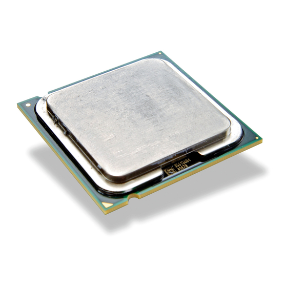
Package Mechanical Specifications Package Mechanical Specifications The processor is packaged in a Flip-Chip Land Grid Array (FC-LGA6) package that interfaces with the motherboard via an LGA775 socket. The package consists of a processor core mounted on a substrate land-carrier. An integrated heat spreader (IHS) is attached to the package substrate and core and serves as the mating surface for processor component thermal solutions, such as a heatsink. -
Page 36: Processor Package Drawing Sheet 1 Of 3
Package Mechanical Specifications Figure 8. Processor Package Drawing Sheet 1 of 3 Datasheet... -
Page 37: Processor Package Drawing Sheet 2 Of 3
Package Mechanical Specifications Figure 9. Processor Package Drawing Sheet 2 of 3 Datasheet... -
Page 38: Processor Package Drawing Sheet 3 Of 3
Package Mechanical Specifications Figure 10. Processor Package Drawing Sheet 3 of 3 Datasheet... -
Page 39: Processor Component Keep-Out Zones
Package Mechanical Specifications 3.1.1 Processor Component Keep-Out Zones The processor may contain components on the substrate that define component keep- out zone requirements. A thermal and mechanical solution design must not intrude into the required keep-out zones. Decoupling capacitors are typically mounted to either the topside or land-side of the package substrate. -
Page 40: Package Insertion Specifications
15show the topside markings on the processor. The diagrams are to aid in the identification of the processor. ® Figure 11. Processor Top-Side Markings Example for the Intel Core™2 Duo Desktop Processor E6000 Series with 4 MB L2 Cache with 1333 MHz FSB INTEL ©'05 E6850... -
Page 41: Core™2 Duo Desktop
Package Mechanical Specifications ® Figure 12. Processor Top-Side Markings Example for the Intel Core™2 Duo Desktop Processors E6000 Series with 4 MB L2 Cache with 1066 MHz FSB INTEL ©'05 INTEL® CORE™2 DUO 6700 SLxxx [COO] 2.66GHZ/4M/1066/06 [FPO] ATPO ®... -
Page 42: Processors E4000 Series With 2 Mb L2 Cache
Package Mechanical Specifications ® Figure 14. Processor Top-Side Markings Example for the Intel Core™2 Duo Desktop Processors E4000 Series with 2 MB L2 Cache INTEL ©'05 E4500 INTEL® CORE™2 DUO SLxxx [COO] 2.20GHZ/2M/800/06 [FPO] ATPO ® Figure 15. Processor Top-Side Markings for the Intel Core™2 Extreme Processor X6800... -
Page 43: Processor Land Coordinates
Package Mechanical Specifications 3.1.8 Processor Land Coordinates Figure 16 shows the top view of the processor land coordinates. The coordinates are referred to throughout the document to identify processor lands. Figure 16. Processor Land Coordinates and Quadrants (Top View) Preliminary Address/ Socket 775 Common Clock/... - Page 44 Package Mechanical Specifications Datasheet...
-
Page 45: Land Listing And Signal Descriptions
Land Listing and Signal Descriptions Land Listing and Signal Descriptions This chapter provides the processor land assignment and signal descriptions. Processor Land Assignments This section contains the land listings for the processor. The land-out footprint is shown Figure 17 Figure 18. -
Page 46: Land-Out Diagram (Top View - Left Side)
Land Listing and Signal Descriptions Figure 17. land-out Diagram (Top View – Left Side) FC34 FC31 BSEL1 FC15 FC33 FC32 BSEL2 BSEL0 BCLK1 TESTHI4 TESTHI5 TESTHI3 TESTHI6 RESET# D47# D44# DSTBN2# DSTBP2# D35# D36# D32# D31# RSVD BCLK0 VTT_SEL TESTHI0 TESTHI2 TESTHI7 RSVD... -
Page 47: Land-Out Diagram (Top View - Right Side)
Land Listing and Signal Descriptions Figure 18. land-out Diagram (Top View – Right Side) VID_SELE VSS_MB_ VCC_MB_ VSS_ VCC_ REGULATION REGULATION SENSE SENSE VID7 FC40 VID6 VID2 VID0 VID3 VID1 VID5 VRDSEL PROCHOT# THERMDA VID4 ITP_CLK0 THERMDC A35# A34# ITP_CLK1 BPM0# BPM1# A33#... -
Page 48: Alphabetical Land Assignments
Land Listing and Signal Descriptions Table 23. Alphabetical Land Table 23. Alphabetical Land Assignments Assignments Land Signal Buffer Land Signal Buffer Land Name Direction Land Name Direction Type Type Source Synch Input/Output BNR# Common Clock Input/Output Source Synch Input/Output BPM0# Common Clock Input/Output Source Synch Input/Output BPM1#... - Page 49 Land Listing and Signal Descriptions Table 23. Alphabetical Land Table 23. Alphabetical Land Assignments Assignments Land Signal Buffer Land Signal Buffer Land Name Direction Land Name Direction Type Type D22# Source Synch Input/Output D61# Source Synch Input/Output D23# Source Synch Input/Output D62# Source Synch Input/Output D24#...
- Page 50 Land Listing and Signal Descriptions Table 23. Alphabetical Land Table 23. Alphabetical Land Assignments Assignments Land Signal Buffer Land Signal Buffer Land Name Direction Land Name Direction Type Type FC33 Power/Other RESERVED FC34 Power/Other RESERVED FC35 Power/Other RESERVED FC36 Power/Other RESERVED FC37 Power/Other...
- Page 51 Land Listing and Signal Descriptions Table 23. Alphabetical Land Table 23. Alphabetical Land Assignments Assignments Land Signal Buffer Land Signal Buffer Land Name Direction Land Name Direction Type Type TRDY# Common Clock Input AF22 Power/Other TRST# Input Power/Other Power/Other Power/Other Power/Other AG11 Power/Other...
- Page 52 Land Listing and Signal Descriptions Table 23. Alphabetical Land Table 23. Alphabetical Land Assignments Assignments Land Signal Buffer Land Signal Buffer Land Name Direction Land Name Direction Type Type AJ18 Power/Other AM19 Power/Other AJ19 Power/Other AM21 Power/Other AJ21 Power/Other AM22 Power/Other AJ22 Power/Other...
- Page 53 Land Listing and Signal Descriptions Table 23. Alphabetical Land Table 23. Alphabetical Land Assignments Assignments Land Signal Buffer Land Signal Buffer Land Name Direction Land Name Direction Type Type Power/Other Power/Other Power/Other Power/Other Power/Other Power/Other Power/Other Power/Other Power/Other Power/Other Power/Other Power/Other Power/Other Power/Other...
- Page 54 Land Listing and Signal Descriptions Table 23. Alphabetical Land Table 23. Alphabetical Land Assignments Assignments Land Signal Buffer Land Signal Buffer Land Name Direction Land Name Direction Type Type VID0 Power/Other Output Power/Other VID1 Power/Other Output Power/Other VID2 Power/Other Output Power/Other VID3 Power/Other...
- Page 55 Land Listing and Signal Descriptions Table 23. Alphabetical Land Table 23. Alphabetical Land Assignments Assignments Land Signal Buffer Land Signal Buffer Land Name Direction Land Name Direction Type Type AG23 Power/Other Power/Other AG24 Power/Other Power/Other Power/Other AL10 Power/Other Power/Other AL13 Power/Other AH10 Power/Other...
- Page 56 Land Listing and Signal Descriptions Table 23. Alphabetical Land Table 23. Alphabetical Land Assignments Assignments Land Signal Buffer Land Signal Buffer Land Name Direction Land Name Direction Type Type Power/Other Power/Other Power/Other Power/Other Power/Other Power/Other Power/Other Power/Other Power/Other Power/Other Power/Other Power/Other Power/Other Power/Other...
- Page 57 Land Listing and Signal Descriptions Table 23. Alphabetical Land Table 23. Alphabetical Land Assignments Assignments Land Signal Buffer Land Signal Buffer Land Name Direction Land Name Direction Type Type Power/Other Power/Other Power/Other Power/Other Power/Other Power/Other Power/Other Power/Other Power/Other VSS_MB_ Power/Other Output REGULATION Power/Other...
-
Page 58: Numerical Land Assignment
Land Listing and Signal Descriptions Table 24. Numerical Land Table 24. Numerical Land Assignment Assignment Land Signal Buffer Land Signal Buffer Land Name Direction Land Name Direction Type Type Power/Other Power/Other RS2# Common Clock Input D13# Source Synch Input/Output D02# Source Synch Input/Output COMP8 Power/Other... - Page 59 Land Listing and Signal Descriptions Table 24. Numerical Land Table 24. Numerical Land Assignment Assignment Land Signal Buffer Land Signal Buffer Land Name Direction Land Name Direction Type Type DBI3# Source Synch Input/Output Power/Other D58# Source Synch Input/Output Power/Other Power/Other Power/Other VCCIOPLL Power/Other...
- Page 60 Land Listing and Signal Descriptions Table 24. Numerical Land Table 24. Numerical Land Assignment Assignment Land Signal Buffer Land Signal Buffer Land Name Direction Land Name Direction Type Type D23# Source Synch Input/Output D44# Source Synch Input/Output D24# Source Synch Input/Output D47# Source Synch Input/Output Power/Other...
- Page 61 Land Listing and Signal Descriptions Table 24. Numerical Land Table 24. Numerical Land Assignment Assignment Land Signal Buffer Land Signal Buffer Land Name Direction Land Name Direction Type Type BSEL1 Power/Other Output Power/Other VTT_OUT_LEFT Power/Other Output Power/Other Power/Other Power/Other FC22 Power/Other Power/Other Power/Other...
-
Page 62: Vcc Cc Static And Transient Tolerance
Land Listing and Signal Descriptions Table 24. Numerical Land Table 24. Numerical Land Assignment Assignment Land Signal Buffer Land Signal Buffer Land Name Direction Land Name Direction Type Type Power/Other Power/Other PWRGOOD Power/Other Input Power/Other IGNNE# Asynch CMOS Input Power/Other Power/Other Power/Other RESERVED... - Page 63 Land Listing and Signal Descriptions Table 24. Numerical Land Table 24. Numerical Land Assignment Assignment Land Signal Buffer Land Signal Buffer Land Name Direction Land Name Direction Type Type Power/Other Power/Other Power/Other A19# Source Synch Input/Output Power/Other Power/Other MSID1 Power/Other Output Power/Other RESERVED...
- Page 64 Land Listing and Signal Descriptions Table 24. Numerical Land Table 24. Numerical Land Assignment Assignment Land Signal Buffer Land Signal Buffer Land Name Direction Land Name Direction Type Type AB26 Power/Other FC18 Power/Other AB27 Power/Other RESERVED AB28 Power/Other Power/Other AB29 Power/Other RESERVED AB30...
- Page 65 Land Listing and Signal Descriptions Table 24. Numerical Land Table 24. Numerical Land Assignment Assignment Land Signal Buffer Land Signal Buffer Land Name Direction Land Name Direction Type Type AF12 Power/Other AG21 Power/Other AF13 Power/Other AG22 Power/Other AF14 Power/Other AG23 Power/Other AF15 Power/Other...
- Page 66 Land Listing and Signal Descriptions Table 24. Numerical Land Table 24. Numerical Land Assignment Assignment Land Signal Buffer Land Signal Buffer Land Name Direction Land Name Direction Type Type AH30 Power/Other Power/Other BPM1# Common Clock Input/Output AK10 Power/Other BPM0# Common Clock Input/Output AK11 Power/Other ITP_CLK1...
- Page 67 Land Listing and Signal Descriptions Table 24. Numerical Land Table 24. Numerical Land Assignment Assignment Land Signal Buffer Land Signal Buffer Land Name Direction Land Name Direction Type Type AL18 Power/Other AM27 Power/Other AL19 Power/Other AM28 Power/Other AL20 Power/Other AM29 Power/Other AL21 Power/Other...
-
Page 68: Alphabetical Signals Reference
Land Listing and Signal Descriptions Alphabetical Signals Reference Table 25. Signal Description (Sheet 1 of 9) Name Type Description A[35:3]# (Address) define a 2 -byte physical memory address space. In sub-phase 1 of the address phase, these signals transmit the address of a transaction. In sub-phase 2, these signals transmit transaction type information. - Page 69 Land Listing and Signal Descriptions Table 25. Signal Description (Sheet 1 of 9) Name Type Description BPM[5:0]# (Breakpoint Monitor) are breakpoint and performance monitor signals. They are outputs from the processor which indicate the status of breakpoints and programmable counters used for monitoring processor performance.
- Page 70 Land Listing and Signal Descriptions Table 25. Signal Description (Sheet 1 of 9) Name Type Description D[63:0]# (Data) are the data signals. These signals provide a 64- bit data path between the processor FSB agents, and must connect the appropriate pins/lands on all such agents. The data driver asserts DRDY# to indicate a valid data transfer.
- Page 71 When STPCLK# is not asserted, FERR#/PBE# is similar to the ERROR# signal on the Intel 387 coprocessor, and is included for compatibility with systems using MS-DOS*-type floating-point error reporting. When STPCLK# is asserted, an...
- Page 72 Land Listing and Signal Descriptions Table 25. Signal Description (Sheet 1 of 9) Name Type Description Input/ HIT# (Snoop Hit) and HITM# (Hit Modified) convey transaction HIT# Output snoop operation results. Any FSB agent may assert both HIT# and HITM# together to indicate that it requires a snoop stall, which can HITM# Input/ be continued by reasserting HIT# and HITM# together.
- Page 73 Land Listing and Signal Descriptions Table 25. Signal Description (Sheet 1 of 9) Name Type Description LOCK# indicates to the system that a transaction must occur atomically. This signal must connect the appropriate pins/lands of all processor FSB agents. For a locked sequence of transactions, LOCK# is asserted from the beginning of the first transaction to the end of the last transaction.
- Page 74 Land Listing and Signal Descriptions Table 25. Signal Description (Sheet 1 of 9) Name Type Description All RESERVED lands must remain unconnected. Connection of these lands to V , or to any other signal (including each other) RESERVED can result in component malfunction or incompatibility with future processors.
- Page 75 Land Listing and Signal Descriptions Table 25. Signal Description (Sheet 1 of 9) Name Type Description In the event of a catastrophic cooling failure, the processor will automatically shut down when the silicon has reached a temperature approximately 20 °C above the maximum T Assertion of THERMTRIP# (Thermal Trip) indicates the processor junction temperature has reached a level beyond where permanent silicon damage may occur.
- Page 76 Land Listing and Signal Descriptions Table 25. Signal Description (Sheet 1 of 9) Name Type Description This input should be left as a no connect in order for the processor VRDSEL Input to boot. The processor will not boot on legacy platforms where this land is connected to V VSS are the ground pins for the processor and should be connected Input...
-
Page 77: Thermal Specifications And Design Considerations
5.1.1 Thermal Specifications To allow for the optimal operation and long-term reliability of Intel processor-based systems, the system/processor thermal solution should be designed such that the processor remains within the minimum and maximum case temperature (T... - Page 78 T ® ® 3. Refer to the “Component Identification Information” section of the Intel Core™2 Extreme and Intel Core™2 Duo Desktop Processor Specification Update for processor specific Idle power.
-
Page 79: Thermal Profile 1
® NOTE: For the Intel Core™2 Duo Desktop processor E6x50 series with 4 MB L2 Cache and ® CPUID = 06FBh, and Intel Core™2 Duo Desktop processor E6540 with 4 MB L2 Cache and CPUID = 06FBh. Figure 19. Thermal Profile 1 ®... -
Page 80: Thermal Profile 2
47.9 54.1 60.1 48.4 54.6 48.9 55.2 ® NOTE: For the Intel Core™2 Duo Desktop processor E6000 series with 4 MB L2 Cache and CPUID = 06F6h. Figure 20. Thermal Profile 2 65.0 60.0 55.0 y = 0.26x + 43.2 50.0... - Page 81 NOTE: For the Intel Core™2 Duo Desktop processor E4000 series with 2 MB L2 Cache and ® CPUID = 06FDh, and for the Intel Core™2 Duo Desktop processor E4700 with 2 MB L2 Cache and CPUID = 06FBh. Figure 21.
-
Page 82: Thermal Profile 4
NOTE: For the Intel Core™2 Duo Desktop processor E6000 and E4000 series with 2 MB L2 ® Cache and CPUID = 06F2h, and for the Intel Core™2 Duo Desktop processor E6000 series with 2 MB L2 Cache and CPUID = 06F6h. -
Page 83: Thermal Profile 5
53.3 59.3 47.8 53.8 59.8 48.3 54.2 60.2 48.7 54.7 60.4 ® NOTE: For the Intel Core™2 Extreme processor X6800. Figure 23. Thermal Profile 5 65.0 60.0 55.0 y = 0.23x + 43.2 50.0 45.0 40.0 Pow er (W ) ®... -
Page 84: Thermal Metrology
26. This temperature specification is meant to help ensure proper operation of the processor. Figure 24 illustrates where Intel recommends T thermal measurements should be made. For detailed guidelines on temperature measurement methodology, refer to the appropriate Thermal and Mechanical Design Guidelines (see Section 1.2). -
Page 85: Thermal Monitor 2
Thermal Specifications and Design Considerations and in some cases may result in a T that exceeds the specified maximum temperature and may affect the long-term reliability of the processor. In addition, a thermal solution that is significantly under-designed may not be capable of cooling the processor even when the TCC is active continuously. -
Page 86: On-Demand Mode
Thermal Specifications and Design Considerations Figure 25. Thermal Monitor 2 Frequency and Voltage Ordering Temperature Frequency PROCHOT# The PROCHOT# signal is asserted when a high temperature situation is detected, regardless of whether Thermal Monitor or Thermal Monitor 2 is enabled. It should be noted that the Thermal Monitor 2 TCC cannot be activated via the on demand mode. -
Page 87: Prochot# Signal
Thermal Specifications and Design Considerations 5.2.4 PROCHOT# Signal An external signal, PROCHOT# (processor hot), is asserted when the processor core temperature has reached its maximum operating temperature. If the Thermal Monitor is enabled (note that the Thermal Monitor must be enabled for the processor to be operating within specification), the TCC will be active when PROCHOT# is asserted. -
Page 88: Thermal Diode
Ω 2, 3, 5 NOTES: Intel does not support or recommend operation of the thermal diode under reverse bias. Characterized across a temperature range of 50 – 80 °C. Not 100% tested. Specified by design characterization. The ideality factor, n, represents the deviation from ideal diode behavior as exemplified by... -
Page 89: Thermal "Diode" Parameters Using Transistor Model
4.52 6.24 Ω 3, 6 NOTES: Intel does not support or recommend operation of the thermal diode under reverse bias. Same as I Table Characterized across a temperature range of 50–80 °C. Not 100% tested. Specified by design characterization. The ideality factor, nQ, represents the deviation from ideal transistor model behavior as... -
Page 90: Platform Environment Control Interface (Peci)
Platform Environment Control Interface (PECI) 5.4.1 Introduction PECI offers an interface for thermal monitoring of Intel processor and chipset components. It uses a single wire, thus alleviating routing congestion issues. Figure 26 shows an example of the PECI topology in a system. PECI uses CRC checking on the host side to ensure reliable transfers between the host and client devices. -
Page 91: Conceptual Fan Control On Peci-Based Platforms
Thermal Specifications and Design Considerations Figure 27. Conceptual Fan Control on PECI-Based Platforms TCC Activation CONTROL Setting Temperature PECI = 0 Fan Speed PECI = -10 (RPM) PECI = -20 Temperature Note: Not intended to depict actual implementation Figure 28. Conceptual Fan Control on Thermal Diode-Based Platforms TCC Activation CONTROL... -
Page 92: Peci Specifications
Thermal Specifications and Design Considerations 5.4.2 PECI Specifications 5.4.2.1 PECI Device Address The PECI device address for the socket is 30h. For more information on PECI domains, refer to the Platform Environment Control Interface Specification. 5.4.2.2 PECI Command Support PECI command support is covered in detail in the Platform Environment Control Interface Specification. -
Page 93: Features
Features Features Power-On Configuration Options Several configuration options can be configured by hardware. The processor samples the hardware configuration at reset, on the active-to-inactive transition of RESET#. For specifications on these options, refer to Table The sampled information configures the processor for subsequent operation. These configuration options cannot be changed except by another reset. -
Page 94: Normal State
LINT[1:0] (NMI, INTR). RESET# causes the processor to immediately initialize itself. The return from a System Management Interrupt (SMI) handler can be to either Normal Mode or the HALT Power Down state. See the Intel Architecture Software Developer's Manual, Volume III: System Programmer's Guide for more information. -
Page 95: Extended Halt Powerdown State
Features The system can generate a STPCLK# while the processor is in the HALT powerdown state. When the system de-asserts the STPCLK# interrupt, the processor will return execution to the HALT state. While in HALT Power powerdown, the processor processes bus snoops. 6.2.2.2 Extended HALT Powerdown State Extended HALT is a low power state entered when all processor cores have executed... -
Page 96: Extended Stop Grant State
Technology. This technology enables the processor to switch between multiple frequency and voltage points, which results in platform power savings. Enhanced Intel SpeedStep Technology requires support for dynamic VID transitions in the platform. Switching between voltage/ frequency states is software controlled. - Page 97 To run at reduced power consumption, the voltage is altered in step with the bus ratio. ® The following are key features of Enhanced Intel SpeedStep Technology: • Multiple voltage/frequency operating points provide optimal performance at reduced power consumption.
- Page 98 Features Datasheet...
-
Page 99: Boxed Processor Specifications
Boxed Processor Specifications Boxed Processor Specifications The processor is also offered as an Intel boxed processor. Intel boxed processors are intended for system integrators who build systems from baseboards and standard components. The boxed processor will be supplied with a cooling solution. This chapter documents baseboard and system requirements for the cooling solution that will be supplied with the boxed processor. -
Page 100: Mechanical Specifications
Boxed Processor Specifications Mechanical Specifications 7.1.1 Boxed Processor Cooling Solution Dimensions This section documents the mechanical specifications of the boxed processor. The boxed processor will be shipped with an unattached fan heatsink. Figure 30 shows a mechanical representation of the boxed processor. Clearance is required around the fan heatsink to ensure unimpeded airflow for proper cooling. -
Page 101: Boxed Processor Fan Heatsink Weight
Boxed Processor Specifications Figure 33. Space Requirements for the Boxed Processor (Overall View) Boxed Proc OverallView 7.1.2 Boxed Processor Fan Heatsink Weight The boxed processor fan heatsink will not weigh more than 550 grams. See Chapter 5 and the appropriate Thermal and Mechanical Design Guidelines (see Section 1.2) for details on the processor weight and heatsink requirements. -
Page 102: Boxed Processor Fan Heatsink Power Cable Connector Description
Boxed Processor Specifications The boxed processor's fanheat sink requires a constant +12 V supplied to pin 2 and does not support variable voltage control or 3-pin PWM control. The power header on the baseboard must be positioned to allow the fan heatsink power cable to reach it. -
Page 103: Thermal Specifications
Boxed Processor Specifications Figure 35. Baseboard Power Header Placement Relative to Processor Socket R110 [4.33] Boxed Proc PwrHeaderPlacement Thermal Specifications This section describes the cooling requirements of the fan heatsink solution used by the boxed processor. 7.3.1 Boxed Processor Cooling Requirements The boxed processor may be directly cooled with a fan heatsink. -
Page 104: Boxed Processor Fan Heatsink Airspace Keepout Requirements (Side 1 View)
Boxed Processor Specifications Figure 36. Boxed Processor Fan Heatsink Airspace Keepout Requirements (side 1 view) Figure 37. Boxed Processor Fan Heatsink Airspace Keepout Requirements (Side 2 View) Datasheet... -
Page 105: Fan Speed Control Operation (Intel Core2 Extreme Processor X6800 Only)
4-pin fan header and must be designed with a fan speed controller with PWM output and Digital Thermometer measurement capabilities. For more information on specific ® motherboard requirements for 4-wire based fan speed control, refer to the Intel ® ®... -
Page 106: Fan Heatsink Power And Signal Specifications
As processor power has increased the required thermal solutions have generated increasingly more noise. Intel has added an option to the boxed processor that allows system integrators to have a quieter system in the most common usage. -
Page 107: Balanced Technology Extended (Btx) Boxed Processor Specifications
(BTX) Boxed Processor Specifications The processor is offered as an Intel boxed processor. Intel boxed processors are intended for system integrators who build systems from largely standard components. The boxed processor will be supplied with a cooling solution known as the Thermal Module Assembly (TMA). -
Page 108: Mechanical Specifications
Balanced Technology Extended (BTX) Boxed Processor Specifications Figure 40. Mechanical Representation of the Boxed Processor with a Type II TMA NOTE: The duct, clip, heatsink and fan can differ from this drawing representation but the basic shape and size will remain the same. Mechanical Specifications 8.1.1 Balanced Technology Extended (BTX) Type I and Type II... -
Page 109: Requirements For The Balanced Technology Extended (Btx) Type I Keep-Out
Balanced Technology Extended (BTX) Boxed Processor Specifications Figure 41. Requirements for the Balanced Technology Extended (BTX) Type I Keep-out Volumes NOTE: Diagram does not show the attached hardware for the clip design and is provided only as a mechanical representation. Datasheet... -
Page 110: Boxed Processor Thermal Module Assembly Weight
Balanced Technology Extended (BTX) Boxed Processor Specifications Figure 42. Requirements for the Balanced Technology Extended (BTX) Type II Keep-out Volume NOTE: Diagram does not show the attached hardware for the clip design and is provided only as a mechanical representation. 8.1.2 Boxed Processor Thermal Module Assembly Weight The boxed processor thermal module assembly for Type I BTX will not weigh more than... -
Page 111: Boxed Processor Support And Retention Module (Srm)
Balanced Technology Extended (BTX) Boxed Processor Specifications 8.1.3 Boxed Processor Support and Retention Module (SRM) The boxed processor TMA requires an SRM assembly provided by the chassis manufacturer. The SRM provides the attach points for the TMA and provides structural support for the board by distributing the shock and vibration loads to the chassis base pan. -
Page 112: Electrical Requirements
Balanced Technology Extended (BTX) Boxed Processor Specifications Electrical Requirements 8.2.1 Thermal Module Assembly Power Supply The boxed processor's Thermal Module Assembly (TMA) requires a +12 V power supply. The TMA will include power cable to power the integrated fan and will plug into the 4- wire fan header on the baseboard. -
Page 113: Balanced Technology Extended (Btx) Mainboard Power Header Placement (Hatched Area)
Balanced Technology Extended (BTX) Boxed Processor Specifications Table 39. TMA Power and Signal Specifications Description Unit Notes +12V: 12 volt fan power supply 10.2 13.8 - Peak Fan current draw — - Fan start-up current draw — — - Fan start-up current draw maximum —... -
Page 114: Thermal Specifications
Balanced Technology Extended (BTX) Boxed Processor Specifications Thermal Specifications This section describes the cooling requirements of the thermal module assembly solution used by the boxed processor. 8.3.1 Boxed Processor Cooling Requirements The boxed processor may be directly cooled with a TMA. However, meeting the processor's temperature specification is also a function of the thermal design of the entire system, and ultimately the responsibility of the system integrator. -
Page 115: Boxed Processor Tma Set Points
As processor power has increased, the required thermal solutions have generated increasingly more noise. Intel has added an option to the boxed processor that allows system integrators to have a quieter system in the most common usage. - Page 116 Balanced Technology Extended (BTX) Boxed Processor Specifications the motherboard that sends out a PWM control signal to the 4 pin of the connector labeled as CONTROL. The fan speed is based on a combination of actual processor temperature and thermistor temperature. If the 4-wire PWM controlled fan in the TMA solution is connected to a 3-pin baseboard processor fan header it will default back to a thermistor controlled mode, allowing compatibility with existing 3-pin baseboard designs.
-
Page 117: Debug Tools Specifications
Debug Tools Specifications Logic Analyzer Interface (LAI) Intel is working with two logic analyzer vendors to provide logic analyzer interfaces (LAIs) for use in debugging systems. Tektronix and Agilent should be contacted to get specific information about their logic analyzer interfaces. The following information is general in nature. - Page 118 Debug Tools Specifications Datasheet...
Need help?
Do you have a question about the CORE 2 DUO E4000 - DATASHEET 3-2008 and is the answer not in the manual?
Questions and answers