
Related Manuals for Advantech MIO-5354


Summary of Contents for Advantech MIO-5354
- Page 1 User Manual MIO-5354 Intel® Atom™ x7000RE Series and Intel® Core™ i3-N305 and Intel® Processor N97 on 3.5'' SBC (Code Name: Amston Lake / Alder Lake-N)
- Page 2 No part of this manual may be reproduced, copied, translated, or transmitted in any form or by any means without the prior written permission of Advantech Co., Ltd. The information provided in this manual is intended to be accurate and reliable.
-
Page 3: Product Warranty (2 Years)
Product Warranty (2 Years) Advantech warrants the original purchaser that each of its products will be free from defects in materials and workmanship for two years from the date of purchase. This warranty does not apply to any products that have been repaired or altered by persons other than repair personnel authorized by Advantech, or products that have been subject to misuse, abuse, accident, or improper installation. -
Page 4: Declaration Of Conformity
Discard used batteries according to the manufacturer's instructions. Technical Support and Assistance Visit the Advantech web site at www.advantech.com/support where you can find the latest information about the product. Contact your distributor, sales representative, or Advantech's customer service center for technical support if you need additional assistance. Please have the following information ready before you call: –... -
Page 5: Packing List
Before setting up the system, check that the items listed below are included and in good condition. If any item does not accord with the table, please contact your dealer immediately. 1 x MIO-5354 SBC 1 x SATA Cable 30 cm (P/N: 1700006291) ... - Page 6 MIO-5354 User Manual...
-
Page 7: Table Of Contents
Table 3.1: Connector and Header List........10 Switches and Jumpers ................10 Table 3.2: Switches and Jumpers ..........10 Connector Locations ................11 Figure 3.1 MIO-5354 Connector Locations (Top Side)....11 Figure 3.2 MIO-5354 Connector Locations (Bottom Side)..11 Setting Jumpers ..................12 3.4.1 DC Input Connector (DCIN2) ............ - Page 8 Assignments......73 System I/O Ports..................74 Table A.1: System I/O Ports ............74 1st MB Memory Map................74 Table A.2: 1st MB Memory Map ..........74 Interrupt Assignments ................75 Table A.3: Interrupt Assignments ..........75 MIO-5354 User Manual viii...
-
Page 9: Chapter 1 General Information
Chapter General Information This chapter gives background information on the MIO-5354. Sections include: Introduction Specifications Block Diagram... -
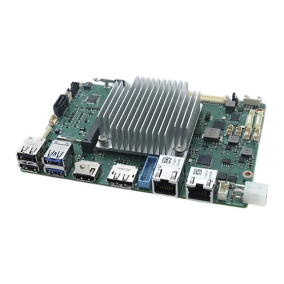
Page 10: Introduction
Introduction MIO-5354 is a 3.5-inch (146 x 102 mm) single-board computer and is powered by Intel Atom® Processors x7000RE Series, Intel® Core™ i3-N305 Processors and Intel® Processor N97. The MIO-5354 can operate under -40~85°C extreme tempera- tures with a x7000RE series SoC and supports a wide power input range of 12~24V. - Page 11 Operating: 40°C @ 95% relative humidity, non-condensing Vibration 3.5 Grms Resistance Certification EMC CE, FCC Class B, ESD 8KV/15KV Criteria A Dimensions 146 x 102 mm (5.7" x 4") Mechanical Net Weight 145 g *Note: Support by Request MIO-5354 User Manual...
-
Page 12: Block Diagram
NC-SI EIO-300 2 x COM CAN1/ CAN2/ GPIO 2 x COM Front Panel Smart FAN RS-232/422/485 CAN-FD CAN-FD (*Opt. SMBus) RS-232, 4wire 8wire *Optional PoE support on LAN2 requires external power module: MIOe-PSE Figure 1.1 Block Diagram MIO-5354 User Manual... -
Page 13: Chapter 2 Mechanical
Chapter Mechanical This chapter gives mechanical information for the MIO-5354. Sections include: Mechanical Drawings... -
Page 14: Board Layout: Dimensions
Board Layout: Dimensions 102.0 98.7 92.7 82.5 31.5 27.2 20.5 Figure 2.1 Mechanical Drawing (Top Side) 102.0 98.7 92.7 27.2 20.5 Figure 2.2 Mechanical Drawing (Bottom Side) MIO-5354 User Manual... - Page 15 16.2 10.6 Figure 2.3 Mechanical Drawing (Coastline) 102.0 98.7 92.7 82.5 31.5 27.2 20.5 Figure 2.4 Mechanical Drawing with Heatsink (Top Side) 24.0 16.2 10.6 Figure 2.5 Mechanical Drawing with Heatsink (Coastline) MIO-5354 User Manual...
- Page 16 102.0 98.7 92.7 82.5 31.5 27.2 20.5 Figure 2.6 Mechanical Drawing with Cooler (Top Side) 25.8 16.2 10.6 Figure 2.7 Mechanical Drawing with Cooler (Coastline) MIO-5354 User Manual...
-
Page 17: Chapter 3 Installation
Chapter Installation This chapter explains the setup procedures for the MIO-5354 hard- ware, including instructions on setting jumpers and connecting peripherals, switches, and indica- tors. Be sure to read all safety pre- cautions before you begin the installation procedure. -
Page 18: Connector And Header List
M.2 B-Key (SATA / PCIe x1) M2_B2 M.2 B-Key (PCIe x1 + USB 2.0) M2_E1 RTC Battery Connector BAT1 Switches and Jumpers Table 3.2: Switches and Jumpers Description Location Name Multifunction Switch JCMOS1 Panel Voltage Selection VDD1 MIO-5354 User Manual... -
Page 19: Connector Locations
LVDS1 VDD1 JCMOS1 FAN1 GPIO1 AUDIO1 COM1 SATAP1 COM2 COM3 SATA1 COM4 CANBUS1 I2C_SMB1 CANBUS2 DCIN2 POE_PWR1 USB1 Figure 3.1 MIO-5354 Connector Locations (Top Side) BAT1 M2_B2 SIM1 M2_E1 M2_B1 Figure 3.2 MIO-5354 Connector Locations (Bottom Side) MIO-5354 User Manual... -
Page 20: Setting Jumpers
Generally, you simply need a standard cable to make most connections. 3.4.1 DC Input Connector (DCIN2) Table 3.3: DC Input Connector Signal Pin Definition +V12_DC_IN +V12_DC_IN MIO-5354 User Manual... -
Page 21: Internal Usb 3.1 Gen1 Connector (Usb1)
3.4.2 Internal USB 3.1 Gen1 Connector (USB1) Table 3.4: Internal USB 3.1 Gen1 Connector Signal Pin Definition Vbus IntA_P1_SSRX- IntA_P1_SSRX+ IntA_P1_SSTX- IntA_P1_SSTX+ IntA_P1_D- IntA_P1_D+ IntA_P2_D+ IntA_P2_D- IntA_P2_SSTX+ IntA_P2_SSTX- IntA_P2_SSRX+ IntA_P2_SSRX- Vbus No Pin MIO-5354 User Manual... -
Page 22: Com Port Connector (Com1)
Table 3.5: COM Port Connector (COM1) Signal Pin Definition COM1_z_RI# COM1_DTR# COM1_CTS# COM1_TXD COM1_RTS# COM1_RXD COM1_DSR# COM1_DCD# 3.4.4 COM Port Connector (COM2) Table 3.6: COM Port Connector (COM2) Signal Pin Definition COM2_RI# COM2_DTR# COM2_CTS# COM2_TXD COM2_RTS# COM2_RXD COM2_DSR# COM2_DCD# MIO-5354 User Manual... -
Page 23: Com Port Connector (Com3)
COM3_RS232-RTS# COM3_RS232-RXD COM3_RS232-CTS# 3.4.6 COM Port Connector (COM4) Table 3.8: COM Port Connector (COM4) Signal Pin Definition COM4_RS232-TXD COM4_RS232-RTS# COM4_RS232-RXD COM4_RS232-CTS# 3.4.7 CAN Bus Connector (CANBUS1) Table 3.9: CAN Bus Connector (CANBUS1) Signal Pin Definition CAN1_D+ CAN1_D- MIO-5354 User Manual... -
Page 24: Can Bus Connector (Canbus2)
CAN Bus Connector (CANBUS2) Table 3.10: CAN Bus Connector (CANBUS2) Signal Pin Definition CAN2_D+ CAN2_D- 3.4.9 Audio Connector (AUDIO1) Table 3.11: Audio Connector (AUDIO1) Signal Pin Definition LOUTR LINR LOUTL LINL MIC1R MIC1L 3.4.10 LVDS Connector (LVDS1) MIO-5354 User Manual... - Page 25 Table 3.12: LVDS Connector (LVDS1) Signal Pin Definition +V_LCD +V_LCD +V_LCD +V_LCD LVDS1_0_D0- LVDS1_1_D0- LVDS1_0_D0+ LVDS1_1_D0+ LVDS1_0_D1- LVDS1_1_D1- LVDS1_0_D1+ LVDS1_1_D1+ LVDS1_0_D2- LVDS1_1_D2- LVDS1_0_D2+ LVDS1_1_D2+ LVDS1_0_CLK- LVDS1_1_CLK- LVDS1_0_CLK+ LVDS1_1_CLK+ LVDS0_DDCCLK_AUX+ LVDS0_DDCDAT_AUX- LVDS1_0_D3- LVDS1_1_D3- LVDS1_0_D3+ LVDS1_1_D3+ LVDS1_VCON MIO-5354 User Manual...
-
Page 26: I2C/Smb Connector (I2C_Smb1)
C/SMB Connector (I C_SMB1) Signal Pin Definition EC_SMB0_z_DAT EC_SMB0_z_CLK +V3.3_DUAL 3.4.12 Fan Connector (FAN1) Table 3.14: Fan Connector (FAN1) Signal Pin Definition +V12 FAN_SPEED FAN_V5_PWM 3.4.13 SATA Power Connector (SATAP1) Table 3.15: SATA Power Connector (SATAP1) Signal Pin Definition MIO-5354 User Manual... -
Page 27: Panel Inverter Connector (Bl1)
Panel Inverter Connector (BL1) Table 3.16: Panel Inverter Connector (BL1) Signal Pin Definition +V12_1_INVERTER_0 LVDS1_Z_ENABKL EC_LVDS1_Z_PWM +V5_1_INVERTER_0 3.4.15 GPIO Connector (GPIO1) Table 3.17: GPIO Connector (GPIO1) Signal Pin Definition SIO_GPIO7 SIO_GPIO2 SIO_GPIO6 SIO_GPIO1 SIO_GPIO5 SIO_GPIO0 SIO_GPIO4 +V5A_GPIO SIO_GPIO3 MIO-5354 User Manual... -
Page 28: Power / Led / Case Open / Buzzer Connector (Fp1)
M.2 B-Key (M2_B1) Table 3.19: M.2 B-Key (M2_B1) Signal Pin Definition Signal Pin Definition 3.3V (Suspend) CONFIG_2 3.3V (Suspend) 3.3V (Suspend) SUSCLK (3.3V) CONFIG_1 RESET# (1.8V) PEWAKE# (3.3V) REFCLKp CLKREQ# (3.3V) REFCLKn PERST# (3.3V) PERp0 PERn0 PETp0 PETn0 MIO-5354 User Manual... -
Page 29: B-Key (M2_B2)
Table 3.20: M.2 B-Key (M2_B2) Signal Pin Definition Signal Pin Definition 3.3V (Suspend) CONFIG_2 3.3V (Suspend) 3.3V (Suspend) SUSCLK (3.3V) CONFIG_1 PEWAKE# (3.3V) REFCLKp CLKREQ# (3.3V) REFCLKn PERST# (3.3V) PERp0 / SATA-A+ PERn0 / SATA-A- PETp0 / SATA-B- PETn0 / SATA-B+ MIO-5354 User Manual... -
Page 30: E-Key (M2_E1)
3.4.19 M.2 E-Key (M2_E1) Table 3.21: M.2 E-Key (M2_E1) Signal Pin Definition Signal Pin Definition 3.3V (Suspend) 3.3V (Suspend) W_DISABLE1# (3.3V) W_DISABLE2# (3.3V) PEWAKE0# (3.3V) PERST0# (3.3V) CLKREQ0# (3.3V) SUSCLK (3.3V) REFCLKn0 REFCLKp0 PETn0 PETp0 PERn0 PERp0 MIO-5354 User Manual... -
Page 31: Rtc Battery Connector (Bat1)
Table 3.21: M.2 E-Key (M2_E1) M2B1_SATA_DEVSLP_R 30 M2B1_SATA_DEVSLP_R 3.3V (Suspend) USB_D- 3.3V (Suspend) USB_D+ 3.4.20 RTC Battery Connector (BAT1) Table 3.22: RTC Battery Connector (BAT1) Signal Pin Definition +VBAT_b1 MIO-5354 User Manual... -
Page 32: Multifunction Switch (Jcmos1)
Multifunction Switch (JCMOS1) Table 3.23: Multifunction Switch (JCMOS1) Function Switch Settings AT/ATX selection *AT mode ATX mode Load CMOS Date *Normal Load BIOS Default COM1 TERM RX Enable *Disable Enable COM2 TERM RX Enable *Disable Enable *Default Setting MIO-5354 User Manual... -
Page 33: Panel Voltage Selection (Vdd1)
Panel Voltage Selection (VDD1) Table 3.24: Panel Voltage Selection Function Jumper Setting Panel Voltage Setting: +V3.3 (Default) Panel Voltage Setting: +V5 Panel Voltage Setting: +V12 Table 3.25: Panel Voltage Selection (VDD1) Signal Pin Definition +V3.3 +V_LVDS_LCD +V12 MIO-5354 User Manual... - Page 34 MIO-5354 User Manual...
-
Page 35: Ami Bios Setup
Chapter AMI BIOS Setup... -
Page 36: Entering Setup
AMIBIOS has been integrated into a plethora of motherboards for decades. With the AMIBIOS Setup program, you can modify BIOS settings and control various system features. This chapter describes the basic navigation of the MIO-5354 BIOS setup screens. AMI BIOS ROM has a built-in Setup program that allows users to modify the basic system configuration. -
Page 37: Main Setup
System Date using the <Arrow> keys. Enter new values through the keyboard. Press the <Tab> key or the <Arrow> keys to move between fields. The date must be entered in MM/DD/YY format. The time must be entered in HH:MM:SS format. MIO-5354 User Manual... -
Page 38: Advanced Bios Features Setup
4.1.2 Advanced BIOS Features Setup Select the Advanced tab from the MIO-5354 Setup screen to enter the Advanced BIOS Setup screen. You can select any of the items in the left frame of the screen, such as CPU Configuration, to go to the sub-menu for that item. You can display an Advanced BIOS Setup option by highlighting it using the <Arrow>... - Page 39 Choose if the ASPM feature is controlled by the OS or BIOS. BDAT ACPI Table Support Enable/Disable support for the BDAT ACPI Table. Low Power S0 Idle Capability Enable/Disable ACPI Low Power S0 Idle Capability under the OS. MIO-5354 User Manual...
- Page 40 4.1.2.2 WWAN Configuration WWAN Device Select the M.2 WWAN Device options to enable 5G-M80 (MediaTek) Modems. 4.1.2.3 CPU Configuration C6DRAM MIO-5354 User Manual...
- Page 41 Number of E-cores to enable in each processor package. Enable/Disable AES (Advanced Encryption Standard). MachineCheck Enable/Disable Machine Check. MonitorMWait Enable/Disable MonitorMWait. Intel® Trusted Execution Technology Enables utilization of additional hardware capability provided by Intel® Trusted Execution Technology. MIO-5354 User Manual...
- Page 42 4.1.2.4 Power & Performance CPU – Power Management Control CPU – Power Management Control Options. GT – Power Management Control GT – Power Management Control Options. CPU - Power Management Control MIO-5354 User Manual...
- Page 43 View/Configure Turbo Ratio Limit Options. Energy Efficient P-state Enable/Disable the Energy Efficient P-state feature. Package Power Limit MSR Lock Enable/Disable locking of Package Power Limit settings. Energy Efficient Turbo Enable/Disable the Energy Efficient Turbo feature. MIO-5354 User Manual...
- Page 44 Current Turbo Ratio Limit Settings – E-core Turbo Ratio Limit Numcore x Efficient-core Turbo Ratio Limit Numcore x defines the core range. MIO-5354 User Manual...
- Page 45 GT - Power Management Control RC6(Render Standby) Check to enable render standby support. Maximum GT frequency Maximum GT frequency limited by user. Disable Turbo GT frequency Enable/Disable Turbo GT frequency. MIO-5354 User Manual...
- Page 46 ME Unconfig on RTC Clear When Disabled, ME will not be unconfigured on RTC Clear. Core BIOS Done Message Enable/Disable Core BIOS Done message sent to ME. Firmware Update Configuration Configure Management Engine Technology Parameters. MIO-5354 User Manual...
- Page 47 Firmware Update Configuration – ME FW Image Re-Flash Enable/Disable ME FW Image Re-Flash function. – FW Update Enable/Disable ME FW Update function. MIO-5354 User Manual...
- Page 48 Allow more than two frequency ranges to be supported. Low Power S0 Idle Capability This variable determines if we enable ACPI Lower Power S0 Idle Capability (Mutually exclusive with Smart connect). While this is enabled, it also disables the 8254 timer for SLP_S0 support. MIO-5354 User Manual...
- Page 49 PCI Express Configuration Setting. Intel ® TCC Authentication – Intel® TCC Authentication determines the key to be used. OEM Enrolled Key is built in by the OEM. Non-OEM Enrolled Key can be added by the user. MIO-5354 User Manual...
- Page 50 TPM 1.2 will restrict support to TPM 1.2 devices. TPM 2.0 will restrict support to TPM 2.0 devices. Auto will support both with the default set to TPM 2.0 devices. If not found, TPM 1.2 devices will be enumerated. MIO-5354 User Manual...
- Page 51 OS. ACPI Sleep State Select the highest ACPI sleep state the system will enter when the SUSPEND button is pressed. PCIE Wake Enable or disable PCIE to wake the system from S5. MIO-5354 User Manual...
- Page 52 Set Parameters of Serial Port 2 (COMB). Serial Port 3 Configuration Set Parameters of Serial Port 3 (COMC). Serial Port 4 Configuration Set Parameters of Serial Port 4 (COMD). Hardware Monitor Monitor hardware Status. Watch Dog Timer Configuration MIO-5354 User Manual...
- Page 53 Enable or Disable USB2_1 Rear Port Power in S4/S5. Serial Port 1 Configuration Serial Port Enable or Disable Serial Port (COM). Change Settings Select an optimal settings for a Super IO device. COM Port Mode COM Port Mode Select. MIO-5354 User Manual...
- Page 54 Serial Port 2 Configuration Serial Port Enable or Disable Serial Port (COM). Change Settings Select an optimal setting for a Super IO device. COM Port Mode COM Port Mode Select. MIO-5354 User Manual...
- Page 55 Serial Port 3 Configuration Serial Port Enable or Disable Serial Port (COM). Change Settings Select optimal settings for a Super IO device. MIO-5354 User Manual...
- Page 56 Serial Port 4 Configuration Serial Port Enable or Disable Serial Port (COM). Change Settings Select optimal settings for a Super IO device. MIO-5354 User Manual...
- Page 57 HW Monitor CPU Temperature System Temperature CPU FAN Speed VBAT The Voltage of RTC Battery. +Vin The Voltage of System DC-IN. MIO-5354 User Manual...
- Page 58 Watch Dog Timer Configuration Watch Dog Timer Enabled or Disabled Watch Dog Timer Function (Start before boot to OS and must stop by self). GPIO Configuration MIO-5354 User Manual...
- Page 59 GPIO Control Enable Choose to control GPIO by EC or user override during POST stage. EdgeBMC Network Configuration EdgeBMC Network Configuration MIO-5354 User Manual...
- Page 60 4.1.2.10 S5 RTC Wake Settings Wake system from S5 Enable/Disable System wake-on-alarm event. Select FixedTime for the system to wake at the hr:min:sec specified. 4.1.2.11 Serial Port Console Redirection MIO-5354 User Manual...
- Page 61 When Bootloader is selected, the Legacy Console Redirection is disabled before booting to a legacy OS. When Always Enable is selected, then Legacy Console Redirection is enabled for legacy OS. Default setting fir this option is set to Always Enable. MIO-5354 User Manual...
- Page 62 Maximum time the device will take before it properly reports itself to the Host Controller. 'Auto' uses the default value: for a Root port it is 100 ms, for a Hub port the delay is taken from the Hub descriptor. MIO-5354 User Manual...
- Page 63 4.1.2.13 Network Stack Configuration Network Stack Enable/Disable UEFI Network Stack. 4.1.2.14 NVMe Configuration MIO-5354 User Manual...
-
Page 64: Chipset Configuration
4.1.3 Chipset Configuration Select the Chipset tab from the MIO-5354 setup screen to enter the Chipset BIOS Setup screen. You can display a Chipset BIOS Setup option by highlighting it using the <Arrow> keys. All Plug and Play BIOS Setup options are described in this sec- tion. - Page 65 Enable/Disable above 4GB Memory Mapped IO BIOS assignment. Memory Configuration Memory Test on Warm Boot Enable/Disable Base Memory Test Run on Warm Boot. Max TOLUD Maximum Value of TOLUD. SA GV System Agent Geyserville. MIO-5354 User Manual...
- Page 66 Graphics turbo IMON current values supported. GTT Size Select the GTT Size. Aperture Size Select the Aperture Size. PSMI Support Enable/Disable PSMI. DVMT Pre-Allocated Select DVMT 5.0 Pre-Allocated (Fixed) Graphics Memory size used by the Internal Graphics Device. MIO-5354 User Manual...
- Page 67 DMI/OPI Configuration DMI Gen3 ASPM DMI Gen3 ASPM Support. DMI ASPM DMI ASPM Support. MIO-5354 User Manual...
- Page 68 Switch Backlight Control Mode to PWM or DC mode. Brightness PWM Polarity Backlight Control Brightness PWN Polarity for Native or Invert. Brightness Control Enable Choose to control LVDS brightness value by EC or user override during POST stage. MIO-5354 User Manual...
- Page 69 Enable or Disable onboard LAN1’s PXE option ROM. Onboard LAN2 Controller Select to Enable or Disable onboard LAN2 Controller. LAN2 PXE ROM Enable or Disable onboard LAN2’s PXE option ROM. SPD Write Disable Enable/Disable setting SPD Write Disable. MIO-5354 User Manual...
- Page 70 PCI Express Configuration DMI Link ASPM Control This item controls Active State Power Management of the DMI Link. PCI Express Root Port 10/12 PCI Express Port 10/12 Settings. MIO-5354 User Manual...
- Page 71 PCI Express Root Port 10 PCI Express Root Port 10 Control the PCI Express Root Port. ASPM Set the ASPM Level. L1 Substates PCI Express L1 Substates settings. PCIe Speed Configure PCIe Speed. MIO-5354 User Manual...
- Page 72 PCI Express Root Port 12 PCI Express Root Port 12 Control the PCI Express Root Port. ASPM Set the ASPM Level. L1 Substates PCI Express L1 Substates settings. PCIe Speed Configure PCIe Speed. MIO-5354 User Manual...
- Page 73 Enable/Disable SATA Device. SATA Mode Selection Determine how the SATA controller operates. SATA Controller Speed Limit Indicates the maximum speed the SATA controller can support. Aggressive LPM Support Enable PCH to aggressively enter link power state. MIO-5354 User Manual...
- Page 74 USB Configuration USB Overcurrent Select "Enabled" if Overcurrent functionality is used. USB Port Disable Override Selectively Enable/Disable the corresponding USB Port from reporting a device connection to the controller. MIO-5354 User Manual...
- Page 75 Enable will lock bytes 38h-3Fh in the lower/upper 128-byte bank of RTC RAM. BIOS Lock Enable or Disable the PCH BIOS Lock Enable feature. Force unlock on all GPIO pads If Enabled, BIOS will force all GPIO pads to be in the unlock state. MIO-5354 User Manual...
- Page 76 HD Audio Configuration HD Audio Control Detection of the HD-Audio device. Disabled = HDA will be uncondition- ally disabled. Enabled = HDA will be unconditionally enabled. MIO-5354 User Manual...
-
Page 77: Security
4.1.4 Security Select Security Setup from the MIO-5354 Setup main BIOS setup menu. All Security Setup options, such as password protection and virus protection are described in this section. To access the sub-menu for the following items, select the item and press <Enter>: Change Administrator / User Password ... -
Page 78: Secure Boot
Policy variables can be configured by a physically present user without full authentication. Restore Factory Keys Force System to User Mode. Install factory default Secure Boot Key databases. Key Management Enables expert users to modify Secure Boot Policy variables without variable authentication. MIO-5354 User Manual... -
Page 79: Boot
It has no effect on BBS boot options. Load Built-in EFI Shell Load/Unload Internal Built-in EFI Shell image inside the BIOS. (Built-in EFI Shell will still be loaded if no bootable device is found). MIO-5354 User Manual... -
Page 80: Save & Exit
This item allows you to save the changes done so far as user defaults. Restore User Defaults This item allows you to restore the user defaults to all the options. Boot Override Boot device select can override your boot priority. MIO-5354 User Manual... -
Page 81: Appendix A System Assignments
Appendix System Assignments This appendix contains informa- tion of a detailed nature. Sections include: System I/O Ports 1st MB Memory Map Interrupt Assignments... -
Page 82: System I/O Ports
Table A.2: 1st MB Memory Map Addr. Range (Hex) Device E0000h - FFFFFh System board D0000h - DFFFFh PCI Bus C0000h - CFFFFh System board A0000h - BFFFFh PCI Bus A0000h - BFFFFh Intel® HD Graphics 00000h - 9FFFFh System board MIO-5354 User Manual... -
Page 83: Interrupt Assignments
Communications Port (COM1) IRQ5 Communications Port (COM3) IRQ6 Reserved IRQ7 CANBUS IRQ8 System CMOS / Real Time Clock IRQ9 Microsoft ACPI-Compliant System IRQ10 Reserved IRQ11 Reserved IRQ12 Available IRQ13 Numeric Data Processor IRQ14 GPIO Controller IRQ15 Communications Port (COM4) MIO-5354 User Manual... - Page 84 No part of this publication may be reproduced in any form or by any means, electronic, photocopying, recording or otherwise, without prior written permis- sion from the publisher. All brand and product names are trademarks or registered trademarks of their respective companies. © Advantech Co., Ltd. 2024...
Need help?
Do you have a question about the MIO-5354 and is the answer not in the manual?
Questions and answers