Table of Contents
Advertisement
Quick Links
NI PXI-5401
16 MHz Function Generator for PXI
A l l t r a d e m a r k s , b r a n d n a m e s , a n d b r a n d s a p p e a r i n g h e r e i n a r e t h e p r o p e r t y o f t h e i r r e s p e c t i v e o w n e r s .
• C r i t i c a l a n d e x p e d i t e d s e r v i c e s
• I n s t o c k / R e a d y - t o - s h i p
Artisan Scientific Corporation dba Artisan Technology Group is not an affiliate, representative, or authorized distributor for any manufacturer listed herein.
In Stock
New From Surplus Stock
Open Web Page
https://www.artisantg.com/58167-5
• We b u y y o u r e x c e s s , u n d e r u t i l i z e d , a n d i d l e e q u i p me n t
• F u l l - s e r v i c e , i n d e p e n d e n t r e p a i r c e n t e r
Advertisement
Table of Contents

Related Manuals for National Instruments PXI-5401


Summary of Contents for National Instruments PXI-5401
- Page 1 NI PXI-5401 16 MHz Function Generator for PXI In Stock New From Surplus Stock Open Web Page https://www.artisantg.com/58167-5 A l l t r a d e m a r k s , b r a n d n a m e s , a n d b r a n d s a p p e a r i n g h e r e i n a r e t h e p r o p e r t y o f t h e i r r e s p e c t i v e o w n e r s .
- Page 2 Computer-Based Instruments NI 5401 User Manual PXI /PCI Arbitrary Function Generator ™ NI 5401 User Manual May 2001 Edition Part Number 322419B-01...
- Page 3 Singapore 2265886, Spain 91 640 0085, Sweden 08 587 895 00, Switzerland 056 200 51 51, Taiwan 02 2528 7227, United Kingdom 01635 523545 For further support information, see the Technical Support Resources appendix. To comment on the documentation, send e-mail to techpubs@ni.com. Copyright © 1999, 2001 National Instruments Corporation. All rights reserved.
- Page 4 The reader should consult National Instruments if errors are suspected. In no event shall National Instruments be liable for any damages arising out of or related to this document or the information contained in it.
- Page 5 Classification requirements are the same for the Federal Communications Commission (FCC) and the Canadian Department of Communications (DOC). Changes or modifications not expressly approved by National Instruments could void the user’s authority to operate the equipment under the FCC Rules.
- Page 6 Canadian Department of Communications This Class B digital apparatus meets all requirements of the Canadian Interference-Causing Equipment Regulations. Cet appareil numérique de la classe B respecte toutes les exigences du Règlement sur le matériel brouilleur du Canada. Compliance to EU Directives Readers in the European Union (EU) must refer to the Manufacturer's Declaration of Conformity (DoC) for information** pertaining to the CE Mark compliance scheme.
- Page 7 Conventions The following conventions are used in this manual: » The » symbol leads you through nested menu items and dialog box options to a final action. The sequence File»Page Setup»Options directs you to pull down the File menu, select the Page Setup item, and select Options from the last dialog box.
-
Page 8: Table Of Contents
Software Options for Your NI 5401 ................1-9 Software Included with Your NI 5401 ............1-9 Interactive Sources Soft Front Panel..........1-9 NI-FGEN Instrument Driver .............1-10 Additional National Instruments Development Tools........1-10 LabVIEW ..................1-10 LabWindows/CVI ................1-11 ComponentWorks ................1-11 Using the Sources Soft Front Panel to Generate Waveforms ........1-12 Generating Standard Functions ...............1-12... - Page 9 Contents Analog Output ....................... 2-7 SYNC Output and Duty Cycle................ 2-9 Output Attenuation..................2-9 Output Impedance ................... 2-10 Output Enable ....................2-10 Phase-Locked Loops and Board Synchronization............2-11 Analog Filter Correction....................2-12 RTSI/PXI Trigger Lines ....................2-13 Calibration ........................2-15 Appendix A Specifications Appendix B...
-
Page 10: Generating Functions With The Ni 5401
Real-Time System Integration (RTSI) and PXI triggers All NI 5401 devices follow industry-standard Plug and Play specifications on both buses and offer seamless integration with compliant systems. Detailed specifications for the NI 5401 are in Appendix A, Specifications. © National Instruments Corporation NI 5401 User Manual... -
Page 11: Safety Information
If the device is damaged, turn the device off and do not use it until service-trained personnel can check its safety. If necessary, return the device to National Instruments for service and repair to ensure that its safety is not compromised. -
Page 12: Connecting Signals
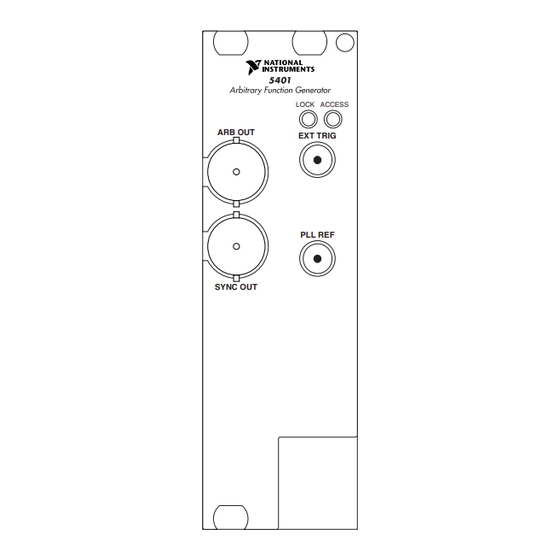
ARB on the PCI version and ARB OUT on the PXI version. LOCK ACCESS ARB OUT EXT TRIG SYNC PLL IN PLL REF SYNC OUT Figure 1-1. NI 5401 I/O Connectors © National Instruments Corporation NI 5401 User Manual... -
Page 13: Arb Connector
Chapter 1 Generating Functions with the NI 5401 ARB Connector The ARB (PCI) or ARB OUT (PXI) connector provides the waveform output. The maximum output levels on this connector depend on the type of load termination. If the output of your NI 5401 terminates into a 50 Ω... -
Page 14: Pll Ref Connector
If no external reference clock is available, the NI 5401 automatically tunes the internal clock to the highest accuracy possible. For more information on PLL operation, refer to Chapter 2, Function Generator Operation. © National Instruments Corporation NI 5401 User Manual... -
Page 15: Pattern Out Connector (Pci Only)
Chapter 1 Generating Functions with the NI 5401 Pattern Out Connector (PCI Only) This connector is used on the NI 5401 for PCI to supply the external trigger input to the board. Connector Pin Assignments Figure 1-4 shows the NI 5401 50-pin digital connector. Refer to Table 1-1 for a description of the signals. -
Page 16: Signal Descriptions
The cable connects to the digital connector on the NI 5401. Figure 1-5 shows the 68-pin connector pin assignments on the SHC50-68 cable. The SHC50-68 connector uses the same signals as the NI 5401 digital output Note connector shown in Table 1-1. © National Instruments Corporation NI 5401 User Manual... - Page 17 Chapter 1 Generating Functions with the NI 5401 DGND DGND DGND DGND DGND DGND DGND DGND DGND DGND DGND DGND DGND DGND DGND DGND DGND DGND DGND DGND DGND DGND DGND DGND DGND DGND DGND DGND DGND DGND DGND DGND DGND EXT_TRIG Figure 1-5.
-
Page 18: Software Options For Your Ni 5401
Sources Soft Front Panel player can then generate. A library of standard waveforms for creating complex waveforms is included, and you can also write equations to create arbitrary waveforms and view the waveforms in a time or frequency domain. © National Instruments Corporation NI 5401 User Manual... -
Page 19: Ni-Fgen Instrument Driver
An NI-FGEN Instrument Driver Quick Reference Guide is included in your NI 5401 kit. This reference guide helps you program your NI 5401. Additional National Instruments Development Tools The following sections describe several additional tools that you can use to develop complex applications for your NI 5401. -
Page 20: Labwindows/Cvi
ComponentWorks features instrumentation-based graphical user interface (GUI) tools, including graphs, meters, gauges, knobs, dials, and switches. Note Use the NI-FGEN instrument driver to program and control your NI 5401 using ComponentWorks. © National Instruments Corporation 1-11 NI 5401 User Manual... -
Page 21: Using The Sources Soft Front Panel To Generate Waveforms
Chapter 1 Generating Functions with the NI 5401 Using the Sources Soft Front Panel to Generate Waveforms You use the Sources Soft Front Panel to interactively control your NI 5401 just as you would a desktop function generator. Generating Standard Functions If you need to generate standard waveforms such as a sine, square, ramp, or DC signal, you can use the Sources Soft Front Panel in the operation mode as shown in Figure 1-6. - Page 22 Configuration to bring up the dialog box shown in Figures 1-7 and 1-8. Figure 1-7. Sources Soft Front Panel Output Settings Dialog Box Figure 1-8. Sources Soft Front Panel Update Clock Settings Dialog Box © National Instruments Corporation 1-13 NI 5401 User Manual...
- Page 23 Chapter 1 Generating Functions with the NI 5401 You can also load a custom waveform pattern. This waveform should be a text, binary, or sound file and should contain exactly 16,384 samples. If the defined waveform does not contain exactly 16,384 samples, the Sources Soft Front Panel either adds the necessary number of 0 values or allows you to choose a subset of the waveform or file.
-
Page 24: Waveform Editor
You can use the Waveform Editor shown in Figure 1-10 to create a custom waveform. To launch the Waveform Editor, select Start»Programs» National Instruments FGEN»Waveform Editor. You can select waveforms from the function library, write equations, or draw them manually. Each segment can have more than one waveform component in it, and you can perform a variety of math functions on each component. -
Page 25: Power-Up And Reset Conditions
Chapter 1 Generating Functions with the NI 5401 Power-Up and Reset Conditions When you power up your computer, the NI 5401 is in the following state: • The output is disabled and set to 0 V. • The trigger mode is set to continuous. •... -
Page 26: Function Generator Operation
Filter, and Sequencer Control Controls Amplifier Analog Filter Trigger SYNC Control Controls Control Level Crossing Detector Data Path PLL Ref PLL and Clocking Interface PXI/PCI Channel Figure 2-1. NI 5401 Block Diagram © National Instruments Corporation NI 5401 User Manual... -
Page 27: Generating Waveforms
Chapter 2 Function Generator Operation The NI 5401 has several main components: • A PXI or PCI bus interface that handles Plug and Play protocols for assigning resources to the device and providing drivers for the data and address bus that are local to the device. •... -
Page 28: Direct Digital Synthesis (Dds)
You can generate sine waves of up to 16 MHz with the NI 5401. Waveform generation always loops back to the beginning of the lookup memory after passing through the end of the lookup memory. © National Instruments Corporation NI 5401 User Manual... -
Page 29: Frequency Hopping And Sweeping
Chapter 2 Function Generator Operation The NI 5401 uses a lookup waveform memory for storing the waveform buffer and FIFO memory for storing the staging list, which contains multiple frequency list information. This FIFO is referred to as an instruction FIFO. Each stage is made up of two instructions: the frequency, which specifies the frequency of the waveform to be generated, and the time, which specifies the time for which the frequency is to be generated. -
Page 30: Modes Of Operation
The last stage is generated repeatedly until you stop the waveform generation. Figure 2-5 illustrates a single trigger mode of operation. © National Instruments Corporation NI 5401 User Manual... -
Page 31: Continuous Trigger Mode
Chapter 2 Function Generator Operation End of All Stages Start Trigger Last Stage Generated f1, ∆T1 f2, ∆T2 f3, ∆T3 Continuously Until Stopped Figure 2-5. Single Trigger Mode For example, assume that one cycle of a sine wave is stored in the DDS lookup memory. -
Page 32: Stepped Trigger Mode
Refer to the Output Enable section in this chapter for additional information about this relay. The output of this relay goes to a series of passive attenuators. © National Instruments Corporation NI 5401 User Manual... - Page 33 Chapter 2 Function Generator Operation The output of the attenuators goes through a selectable output impedance of 50 or 75 Ω to the I/O connector. Figure 2-8 shows the essential block diagram of analog waveform generation. Attenuators 10 dB Lowpass Attenuator (63 dB in 1 dB steps) Filter...
-
Page 34: Sync Output And Duty Cycle
= desired voltage level for the output signal = input voltage level For the NI 5401, V = ±5 V for a terminated load and ±10 V for an Note unterminated load. © National Instruments Corporation NI 5401 User Manual... -
Page 35: Output Impedance
Chapter 2 Function Generator Operation NI-FGEN calculates the value of the output attenuation chain, which you can control by changing the peak-to-peak amplitude parameter. 0 dB attenuation corresponds to an amplitude of 10 V . The maximum pk-pk attenuation of 73 dB corresponds to an amplitude of 2.24 mV pk-pk Any amplitude less then this is coerced to this value. -
Page 36: Phase-Locked Loops And Board Synchronization
(20 MHz) Source Loop Phase Filter Comp Tune PLL Ref (1 V min) pk-pk 80 MHz 20 MHz Div/4 Board Clock VCXO Figure 2-11. PLL Architecture for the NI 5401 for PCI © National Instruments Corporation 2-11 NI 5401 User Manual... -
Page 37: Analog Filter Correction
Chapter 2 Function Generator Operation 10 MHz Osc Source Loop Phase Filter Comp PLL Ref (1 V min) pk-pk 80 MHz 10 MHz Div/8 VCXO Figure 2-12. PLL Architecture for the NI 5401 for PXI You can frequency lock to an external reference clock source of 1 MHz and from 5–20 MHz in 1 MHz increments. -
Page 38: Rtsi/Pxi Trigger Lines
RTSI 3 RTSI RTSI Trigger RTSI 4 Switch RTSI 5 Board Clock RTSI 6 Master/Slave RTSI Osc RTSI Clock Figure 2-14. RTSI Trigger Lines and Routing for the NI 5401 for PCI © National Instruments Corporation 2-13 NI 5401 User Manual... - Page 39 Chapter 2 Function Generator Operation Figure 2-15 shows the PXI trigger lines and routing of NI 5401 for PXI signals to the RTSI switch. TRIG 0 SYNC TRIG 1 Start Trigger TRIG 2 TRIG 3 RTSI RTSI Trigger TRIG 4 Switch BOARD_SYNC TRIG 5...
-
Page 40: Calibration
EEPROM, calculating correction values, and writing those values to the CalDACs. National Instruments calibrates all NI 5401 devices to the levels indicated in Appendix A, Specifications. Factory calibration involves procedures such as nulling the offset and gain errors. However, since offset and gain errors may drift with time and temperature, you may need to recalibrate your device. -
Page 41: Specifications
Voltage Output Ranges ............ ±5 V into a 50 Ω load ±10 V into a high-impedance load Accuracy ..........±0.1 dB Output attenuation........0 to 73 dB Resolution ........0.001 dB steps © National Instruments Corporation NI 5401 User Manual... -
Page 42: Appendix A Specifications
Appendix A Specifications Pre-attenuation offset Range..........±2.5 V into 50 Ω Accuracy..........±5 mV Output coupling ........DC Output impedance........50 Ω or 75 Ω software selectable Load impedance........50 Ω or greater Output enable..........Software switchable Protection..........Short-circuit protected Sine Spectral Purity Harmonic products and spurs Up to 1 MHz........–60 dBc Up to 16 MHz........–35 dBc Phase noise ..........–105 dBc/Hz at 10 kHz from... - Page 43 Trigger to waveform output delay (T )........28 sample clocks + 150 ns max RTSI Trigger lines ........... 7 Clock lines..........1 Bus Interface Type ............Slave Operational Modes Type ............Single, continuous, stepped © National Instruments Corporation NI 5401 User Manual...
-
Page 44: Internal Clock
Appendix A Specifications SYNC Out Level ............TTL Duty cycle..........20% to 80%, software controllable External Clock Reference Input Frequency ..........1 MHz or 5–20 MHz in 1 MHz steps ≤ level ≤ 5 V Amplitude ..........1 V pk-pk pk-pk Internal Clock Frequency ..........40 MHz Initial accuracy ........±5 ppm Temperature stability (0 to 5 °C)....±25 ppm Aging (1 year).........±5 ppm... -
Page 45: Electromagnetic Compatibility
Select the appropriate product family, followed by your product, and a link to the DoC (in Adobe Acrobat format) appears. Click the Acrobat icon to download or read the DoC. © National Instruments Corporation NI 5401 User Manual... -
Page 46: Optional Accessories
Optional Accessories National Instruments offers a variety of products to use with your NI 5401, including probes, cables, and other accessories: • Shielded and unshielded I/O connector blocks (SCB-68, TBX-68, CB-68) • 16 MB memory module (optional) • RTSI bus cables For more specific information about these products, refer to your National Instruments catalogue or web site, or call the office nearest you. -
Page 47: Appendix B Optional Accessories
Appendix B Optional Accessories Table B-1. National Instruments Optional Cable Accessories (Continued) Product Cable Name Part Number Cable Description 50 Ω SMB male to BNC male, 1 m coaxial cable PXI-5401 SMB 110 763405-01 50 Ω SMB male to alligator clip, 1 m cable... -
Page 48: Frequency Resolution And Lookup Memory
On the NI 5401, the maximum frequency of a sine wave you can generate reliably is limited to 16 MHz. Other waveforms, such as square or triangular waves, are limited to 1 MHz. © National Instruments Corporation NI 5401 User Manual... - Page 49 Appendix C Frequency Resolution and Lookup Memory You can also synthesize arbitrary waveforms using DDS. Generating arbitrary waveforms this way will be very limited; you are restricted to a single buffer, and this buffer should be exactly equal to the size of the lookup memory (16,384 samples).
-
Page 50: Technical Support Resources
Technical Support Resources Web Support National Instruments Web support is your first stop for help in solving installation, configuration, and application problems and questions. Online problem-solving and diagnostic resources include frequently asked questions, knowledge bases, product-specific troubleshooting wizards, manuals, drivers, software updates, and more. Web support is available through the Technical Support section of ni.com... -
Page 51: Worldwide Support
Appendix D Technical Support Resources Worldwide Support National Instruments has offices located around the world to help address your support needs. You can access our branch office Web sites from the Worldwide Offices section of . Branch office Web sites provide ni.com... - Page 52 ° degree Ω +5 V +5 V output signal amperes amplification method of scaling the signal level to a higher level normal waveform output signal attenuation decreasing the amplitude of a signal © National Instruments Corporation NI 5401 User Manual...
- Page 53 Glossary bit—one binary digit, either 0 or 1 byte—eight related bits of data, an eight-bit binary number. Also used to denote the amount of memory required to store one byte of data. a type of coaxial signal connector buffer temporary storage for acquired or generated data the group of conductors that interconnect individual circuitry in a computer.
- Page 54 A/D conversion EXT_TRIG external trigger input signal © National Instruments Corporation NI 5401 User Manual...
- Page 55 Glossary FIFO first-in first-out memory buffer—the first data stored is the first data sent to the acceptor. FIFOs are often used on DAQ devices to temporarily store incoming or outgoing data until that data can be retrieved or output. For example, an analog input FIFO stores the results of A/D conversions until the data can be retrieved into system memory, a process that requires the servicing of interrupts and often the programming of the DMA controller.
- Page 56 This method of waveform generation decreases memory requirements. lowpass filter a circuit used to smooth the waveform output and removed unwanted high frequency contents form the signal © National Instruments Corporation NI 5401 User Manual...
- Page 57 Glossary meters (1) Mega, the standard metric prefix for 1 million or 10 , when used with units of measure such as volts and hertz; (2) mega, the prefix for 1,048,576, or 2 , when used with B to quantify data or computer memory master/slave locking the NI 5401 clock in frequency to an external phase locking reference clock source...
- Page 58 For example, a system has 12-bit resolution, one part in 4,096 resolution, and 0.0244 percent of full scale. RTSI bus Real-Time System Integration bus—the National Instruments timing bus that connects DAQ boards directly, by means of connectors on top of the boards, for precise synchronization of functions...
- Page 59 Glossary SCSI Small Computer System Interface (bus) sequence list See staging list. shift-keying frequency shift keying (FSK) single trigger mode when the arbitrary waveform generator goes through the staging list only once Sub Miniature Type B connector that features a snap coupling for fast connection samples per second—used to express the rate at which a DAQ board samples an analog signal...
- Page 60 See linking, looping. word The standard number of bits that a processor or memory manipulates at one time. Microprocessors typically use 8-, 16-, or 32-bit words. © National Instruments Corporation NI 5401 User Manual...
- Page 61 SYNC output and duty cycle, 2-9 DDS. See direct digital synthesis (DDS). block diagram, 2-1 DGND signal (table), 1-7 calibration, 2-15 digital connector signal descriptions (table), 1-7 direct digital synthesis (DDS), 2-3 to 2-4 © National Instruments Corporation NI 5401 User Manual...
- Page 62 Index frequency hopping and sweeping, 2-4 phase-locked loops and board mechanical specifications, A-4 synchronization, 2-11 to 2-12 RTSI/PXI trigger lines, 2-13 to 2-15 triggering, 2-4 to 2-7 continuous trigger mode, 2-6 NI 5401. See also function generator single trigger mode, 2-5 to 2-6 operation.
- Page 63 2-4 DDS output mode (figure), 1-12 timing I/O specifications, A-3 General Settings dialog box (figure), 1-13 trigger specifications generating standard digital trigger, A-3 functions, 1-12 to 1-14 RTSI, A-3 © National Instruments Corporation NI 5401 User Manual...
- Page 64 DDS memory, 1-9 using Waveform Editor, 1-15 waveform memory, lookup, 2-4 Waveform Editor waveform specifications, A-3 creating custom waveforms, 1-15 Web support from National Instruments, D-1 description, 1-9 Worldwide technical support, D-2 NI 5401 User Manual ni.com...
Need help?
Do you have a question about the PXI-5401 and is the answer not in the manual?
Questions and answers