Table of Contents
Advertisement
Quick Links
CALIBRATION PROCEDURE
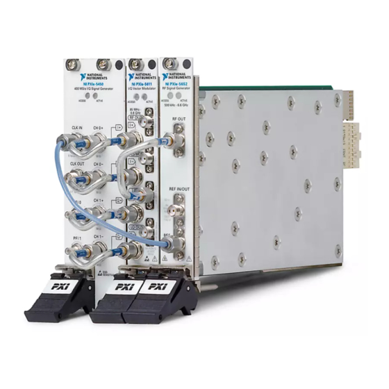
PXIe-5673E
Vector Signal Generator
This document contains the verification procedures for the PXIe-5673E Vector Signal
Generator. Refer to
ni.com/calibration
Contents
Software.................................................................................................................................... 2
Documentation.......................................................................................................................... 2
Calibration Interval................................................................................................................... 2
Test Equipment......................................................................................................................... 3
Test Conditions......................................................................................................................... 4
Initial Setup............................................................................................................................... 5
Test System Characterization ................................................................................................... 5
Characterizing the Power Splitter..................................................................................... 5
As-Found and As-Left Limits................................................................................................... 8
Verification ............................................................................................................................... 8
Verifying LO Output Power Accuracy............................................................................. 9
Verifying Modulation Impairments.................................................................................. 9
Verifying Modulation Bandwidth and Impairments ........................................................ 11
Verifying Output Power Level Accuracy ......................................................................... 14
Verifying Output Intermodulation Products..................................................................... 17
Verifying Noise Floor....................................................................................................... 20
Verifying RF Harmonics .................................................................................................. 21
Verifying Baseband Linearity-Related Spurs................................................................... 23
Verifying Single Sideband Phase Noise at 10 kHz Offset ............................................... 25
Verifying Frequency Accuracy ........................................................................................ 26
Adjustment................................................................................................................................ 27
Reverification ........................................................................................................................... 27
Updating Calibration Date........................................................................................................ 27
Worldwide Support and Services ............................................................................................. 27
for more information about calibration solutions.
Advertisement
Table of Contents

Subscribe to Our Youtube Channel
Related Manuals for National Instruments PXIe-5673E


Summary of Contents for National Instruments PXIe-5673E
-
Page 1: Table Of Contents
CALIBRATION PROCEDURE PXIe-5673E Vector Signal Generator This document contains the verification procedures for the PXIe-5673E Vector Signal Generator. Refer to for more information about calibration solutions. ni.com/calibration Contents Software............................ 2 Documentation.......................... 2 Calibration Interval........................2 Test Equipment......................... 3 Test Conditions......................... 4 Initial Setup.......................... -
Page 2: Software
The measurement accuracy requirements of your application determine how often you should calibrate your device. NI recommends that you perform a complete calibration for the PXIe-5673E at least once a year. You can shorten this calibration interval based on the accuracy demands of your application. -
Page 3: Test Equipment
Frequency range: an MA2472 diode Output power level 50 MHz to 6.6 GHz sensor accuracy Power range: -70 dBm to +10 dBm Accuracy: 0.5% SMA(m)-to-N(f) S.M. Electronics VSWR: 1.15:1 adapter SM4241 PXIe-5673E Calibration Procedure | © National Instruments | 3... -
Page 4: Test Conditions
— — 1 N · m Test Conditions The following setup and environmental conditions are required to ensure the PXIe-5673E meets published specifications. • Verify that the PXIe-5611, PXIe-5450/5451, and PXIe-5650/5651/5652 are properly connected as indicated in the PXIe-5673E Getting Started Guide before starting verification. -
Page 5: Initial Setup
Zero and calibrate the power meter sensors before each test. Initial Setup Refer to the PXIe-5673E Getting Started Guide for information about how to install the software and hardware and how to configure the device in MAX. Test System Characterization Use the following procedures to characterize the test system response. - Page 6 10. Connect the other port of the 6 dB attenuator to the spectrum analyzer RF INPUT front panel connector through the SMA(m)-to-SMA(m) cable as shown in Figure 1. 11. Configure the reference level of the spectrum analyzer to -30 dBm. The spectrum analyzer is used only for termination. 6 | ni.com | PXIe-5673E Calibration Procedure...
- Page 7 • PXIe-5650: 85 MHz to 1.3 GHz • PXIe-5651: 85 MHz to 3.3 GHz • PXIe-5652: 85 MHz to 6.6 GHz Store the resulting measurements as splitter [i] (dB). PXIe-5673E Calibration Procedure | © National Instruments | 7...
-
Page 8: As-Found And As-Left Limits
You have successfully characterized your splitter. As-Found and As-Left Limits The as-found limits are the published specifications for the PXIe-5673E. NI uses these limits to determine whether the PXIe-5673E meets the device specifications when it is received for calibration. -
Page 9: Verifying Lo Output Power Accuracy
Verifying LO Output Power Accuracy Complete the following steps to verify the LO output power accuracy of the PXIe-5673E using a power meter. Connect the PXIe-5611 LO OUT front panel connector to the power meter through the SMA(m)-to-N(f) adapter. Generate a signal with the following niRFSG property settings: •... - Page 10 Center frequency: Equivalent to the frequency in step 4 • Reference level: +5 dBm • Frequency span: 0 Hz • Resolution bandwidth: 500 Hz • Sweep time: 5 ms • Reference clock source: External 10 | ni.com | PXIe-5673E Calibration Procedure...
-
Page 11: Verifying Modulation Bandwidth And Impairments
Connect the PXIe-5611 RF OUT front panel connector to the spectrum analyzer RF INPUT front panel connector through the SMA(m)-to-SMA(m) cable. Connect the PXIe-5650/5651/5652 REF IN/OUT front panel connector to any rubidium frequency reference rear panel BNC connector through the BNC(m)-to-SMA(m) cable. PXIe-5673E Calibration Procedure | © National Instruments | 11... - Page 12 Calculate the relative modulation bandwidth flatness by subtracting the RF output power measured at 0 Hz offset from the RF output powers measured at each of the other offset frequencies. 12 | ni.com | PXIe-5673E Calibration Procedure...
- Page 13 200 MHz 1.3 GHz PXIe-5651/5652 2.4 GHz 3.3 GHz PXIe-5652 4.0 GHz 5.8 GHz If the results are within the selected test limit, the device has passed this portion of the verification. PXIe-5673E Calibration Procedure | © National Instruments | 13...
-
Page 14: Verifying Output Power Level Accuracy
Verifying Output Power Level Accuracy Complete the following steps to verify the output power level accuracy of the PXIe-5673E using a power meter, rubidium frequency standard, spectrum analyzer, power splitter, and 6 dB attenuator. Figure 2. Connecting Hardware to Verify Output Power Level Accuracy... - Page 15 Repeat steps 7 through 8 for the following frequency ranges in 20 MHz increments, including endpoints: • PXIe-5650: 85 MHz to 1.3 GHz • PXIe-5651: 85 MHz to 3.3 GHz • PXIe-5652: 85 MHz to 6.6 GHz Store the resulting measurements. PXIe-5673E Calibration Procedure | © National Instruments | 15...
- Page 16 To maintain the same measurement uncertainty as the power meter, you must Note apply the corrections found in step 12 to the measured results, as shown in the following equation: AdjustedMeasurement [i] = SpecAn [i] + Corrections [i] + Splitter Loss [i] 16 | ni.com | PXIe-5673E Calibration Procedure...
-
Page 17: Verifying Output Intermodulation Products
Complete the following steps to verify the output intermodulation (IMD) performance of an PXIe-5673E using a spectrum analyzer. Complete this test for each iteration in Table 8. Connect the PXIe-5611 RF OUT front panel connector to the spectrum analyzer RF INPUT front panel connector through the SMA(m)-to-SMA(m) cable. - Page 18 Center frequency: (Frequency in step 4) + F • • Reference level: 0 dBm • Frequency span: 0 Hz • Resolution bandwidth: 500 Hz • Sweep time: 5 ms • Reference clock source: External 18 | ni.com | PXIe-5673E Calibration Procedure...
- Page 19 CW Source LO Frequencies R3 Upper Limits (dBc) PXIe-5650/5651/5652 85 MHz to 250 MHz >250 MHz to 1.3 GHz PXIe-5651/5652 >1.3 GHz to 3.3 GHz PXIe-5652 >3.3 GHz to 6.6 GHz PXIe-5673E Calibration Procedure | © National Instruments | 19...
-
Page 20: Verifying Noise Floor
If the results are within the selected test limit, the device has passed this portion of the verification. Verifying Noise Floor Complete the following steps to verify the noise floor performance of an PXIe-5673E module using a spectrum analyzer. Connect the PXIe-5611 RF OUT front panel connector to the spectrum analyzer RF INPUT front panel connector through the SMA(m)-to-SMA(m) cable. -
Page 21: Verifying Rf Harmonics
If the results are within the selected test limit, the device has passed this portion of the verification. Verifying RF Harmonics Complete the following steps to verify the harmonic performance of an PXIe-5673E module using a spectrum analyzer. Connect the PXIe-5611 RF OUT front panel connector to the spectrum analyzer RF INPUT front panel connector through the SMA(m)-to-SMA(m) cable. - Page 22 500 MHz to 3.3 GHz in 50 MHz increments, including endpoints • PXIe-5652: 100 MHz to 500 MHz in 10 MHz increments, including endpoints, and 500 MHz to 6.6 GHz in 50 MHz increments, including endpoints. 22 | ni.com | PXIe-5673E Calibration Procedure...
-
Page 23: Verifying Baseband Linearity-Related Spurs
If the results are within the selected test limit, the device has passed this portion of the verification. Verifying Baseband Linearity-Related Spurs Complete the following steps to verify the baseband-related spur levels of the PXIe-5673E using a spectrum analyzer. Connect the PXIe-5611 RF OUT front panel connector to the spectrum analyzer RF INPUT front panel connector through the SMA(m)-to-SMA(m) cable. - Page 24 >250 MHz to 1.3 GHz PXIe-5651/5652 >1.3 GHz to 3.3 GHz PXIe-5652 >3.3 GHz to 6.6 GHz If the results are within the selected limit, the device has passed this portion of the verification. 24 | ni.com | PXIe-5673E Calibration Procedure...
-
Page 25: Verifying Single Sideband Phase Noise At 10 Khz Offset
Verifying Single Sideband Phase Noise at 10 kHz Offset Complete the following steps to verify the single sideband (SSB) phase noise of the PXIe-5673E using a spectrum analyzer. Connect the PXIe-5611 RF OUT front panel connector to the spectrum analyzer RF INPUT front panel connector through the SMA(m)-to-SMA(m) cable. -
Page 26: Verifying Frequency Accuracy
If the results are within the selected test limit, the device has passed this portion of the verification. Verifying Frequency Accuracy Complete the following steps to verify the frequency accuracy of a PXIe-5673E using a spectrum analyzer. Connect the PXIe-5611 RF OUT front panel connector to the spectrum analyzer RF INPUT front panel connector through the SMA(m)-to-SMA(m) cable. -
Page 27: Adjustment
If the results are within the selected test limit, the device has passed this portion of the verification. Adjustment To adjust the PXIe-5673E to meet published specifications, you must adjust the modules that comprise the PXIe-5673E system. To calibrate the PXIe-5650/5651/5652, PXIe-5450, and PXIe-5611 modules individually, refer to their calibration procedures at ni.com/manuals... - Page 28 For patents covering NI products/technology, refer to the appropriate location: Help»Patents in your software, the patents.txt file on your media, or the National Instruments Patents Notice at ni.com/patents. You can find information about end-user license agreements (EULAs) and third-party legal notices in the readme file for your NI product.
Need help?
Do you have a question about the PXIe-5673E and is the answer not in the manual?
Questions and answers