Table of Contents
Advertisement
Quick Links
DA14535
USB Development Kit Hardware
This document outlines the system design, configuration options, and supported features of DA14535 USB
Development Kit revA (610-12-A).
Contents
Contents ................................................................................................................................................................. 1
Figures .................................................................................................................................................................... 2
Tables ...................................................................................................................................................................... 2
1.
Terms and Definitions .................................................................................................................................... 4
2.
References ...................................................................................................................................................... 4
3.
Introduction ..................................................................................................................................................... 5
4.
System Overview ............................................................................................................................................ 5
4.1
Features .................................................................................................................................................. 5
4.2
System and Components Description (Top View) .................................................................................. 6
4.3
System and Components Description (Bottom View) ............................................................................. 7
5.
USB Kit System .............................................................................................................................................. 8
5.1
Overview.................................................................................................................................................. 8
5.2
DA14535 System .................................................................................................................................... 9
5.3
DA14535 GPIO Assignment.................................................................................................................. 10
5.4
Default Configuration ............................................................................................................................. 11
5.5
1-wire Bootable UART ........................................................................................................................... 12
5.6
Optional 2-/4-Wire UART ...................................................................................................................... 13
5.7
Crystals .................................................................................................................................................. 14
5.8
Antenna and RF Port ............................................................................................................................. 15
5.9
SPI Data Flash Memory (U2) ................................................................................................................ 16
5.10 Reset Circuit .......................................................................................................................................... 17
5.11 General-Purpose Push Button .............................................................................................................. 18
5.12 Debugging Port DIP Switch ................................................................................................................... 19
5.13 MikroBUS™ Module .............................................................................................................................. 20
5.14 User Controlled LED ............................................................................................................................. 21
5.15 GND Test Point ..................................................................................................................................... 21
5.16 Over Voltage Protection Circuit ............................................................................................................. 22
5.17 Debug Interface (U4) ............................................................................................................................. 23
5.18 Power Measurements ........................................................................................................................... 24
5.19 Operation from a Wall Adapter or Power Pack ..................................................................................... 25
5.20 Operation from a Coin Cell Battery ....................................................................................................... 26
5.21 Known Issues ........................................................................................................................................ 26
Appendix A Schematics ...................................................................................................................................... 27
Appendix B Components Placement on PCB ................................................................................................... 29
Appendix C PCB Layer Chart ............................................................................................................................. 30
June 5, 2024
CFR0012
Manual
Page 1
© 2024 Renesas Electronics
Advertisement
Table of Contents

Related Manuals for Renesas DA14535


Summary of Contents for Renesas DA14535
-
Page 1: Table Of Contents
Manual DA14535 USB Development Kit Hardware This document outlines the system design, configuration options, and supported features of DA14535 USB Development Kit revA (610-12-A). Contents Contents ................................. 1 Figures ..................................2 Tables ..................................2 Terms and Definitions ............................ 4 References ..............................4 Introduction .............................. -
Page 2: Figures
Figure 2. USB kit – top side ............................6 Figure 3. USB Kit - bottom side ..........................7 Figure 4. Block diagram of DA14535 USB development kit ..................9 Figure 5. DA14535 section schematic ........................9 Figure 6. Default DIP switch configuration ......................11 Figure 7. - Page 3 DA14535 USB Development Kit Hardware Table 6. RF Components names and values ......................15 Table 7. DIP switch configuration ........................... 19 Table 8. Information provided on PCBA label ......................31 UM-B-182 Revision 1.0 Page 3 June 5, 2024 CFR0012...
-
Page 4: Terms And Definitions
AN-B-052, DA1458x/68x Development kit J-Link Interface, Application Note, Renesas Electronics. AN-B-072, DA1453x Booting Options, Application Note, Renesas Electronics. AN-B-027, Designing Printed Antennas for Bluetooth Smart, Application Note, Renesas Electronics. Note 1 References are for the latest published version, unless otherwise indicated. -
Page 5: Introduction
DA14535 USB Development Kit Hardware 3. Introduction This document describes Renesas DA14535 USB development kit (board reference number 610-12-A). This kit offers a low-cost development board with basic functionality. The development kit is implemented on a single PCB. The block diagram, the actual board, the various sections, and settings as well as the connectivity are presented. -
Page 6: System And Components Description (Top View)
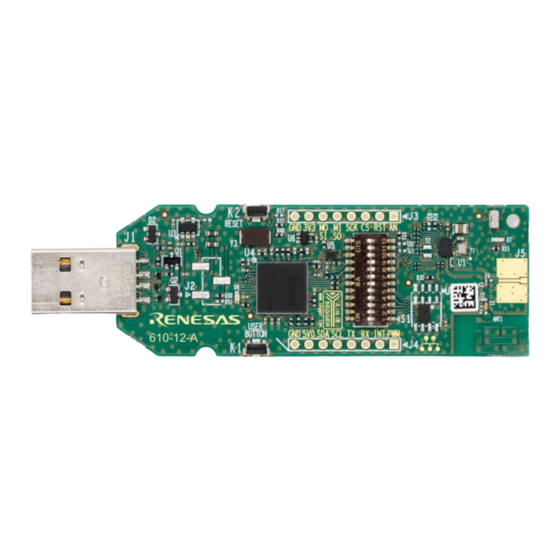
4 5 7 12 13 Figure 2. USB kit – top side This USB development kit is based on the DA14535 SoC in an FCGQFN-24 package. The marked and numbered sections of the system are (see Figure 1. Type-A USB connector (J1). -
Page 7: System And Components Description (Bottom View)
DA14535 USB Development Kit Hardware System and Components Description (Bottom View) Figure 3. USB Kit - bottom side The bottom side of the USB development kit provides information about the mikroBus™ pins assignment, the SEGGER ID, and the date code. Test points have been placed for monitoring various signal behaviors and voltage levels of the components. -
Page 8: Usb Kit System
DA14535 USB Development Kit Hardware 5. USB Kit System Overview ▪ Board name/number: • DA14535 USB development kit/610-12-A. ▪ SoC: • DA14535 in FCGQFN-24 package. ▪ Flash memory: • AT25DF021A, 2 Mbit, QSPI Flash Memory in 8-pin U-SON (2 mm × 3 mm) package. Note that it is accessed in plain SPI mode. -
Page 9: Da14535 System
DA14535 USB Development Kit Hardware DA14535 System Figure 4. Block diagram of DA14535 USB development kit Renesas DA14535 is an ultra-low power SoC integrating a 2.4 GHz Bluetooth Low Energy transceiver and an ® ® Cortex M0+ microcontroller with 48 kB RAM and 32 kB One-Time Programmable (OTP) ROM. It can be used as a standalone application processor or as a data pump in hosted systems. -
Page 10: Da14535 Gpio Assignment
Most of the available signals are utilized or extracted on the breakout connectors. Table 1 shows the pin assignment on the development kit peripheral function and the related pin name on the FCGQFN24 package of the DA14535. Table 1. DA14535 USB development kit pin assignment UART XTAL Single... -
Page 11: Default Configuration
DA14535 USB Development Kit Hardware Default Configuration Because GPIOs P0_0 to P0_6 support multiple functions, the default system is limited to a subset of the possible options. Figure 6 shows the default DIP switch configuration. Figure 6. Default DIP switch configuration This allows the system to boot from external flash or 1-wire UART and communicate through JTAG for debugging. -
Page 12: 1-Wire Bootable Uart
Since most UART communication is typically half-duplex, it is possible to use a single pin for both the Rx and the Tx channel. DA14535 has dedicated hardware that supports this function and two related boot steps predefined. An analog multiplexer shown in... -
Page 13: Optional 2-/4-Wire Uart
DA14535 USB Development Kit Hardware Optional 2-/4-Wire UART It is possible to use a 2-wire or 4-wire UART for booting or other activities, but it is not possible to boot from the SPI flash in this configuration. To enable the UART and disable SPI, it is required to modify the DIP switch as... -
Page 14: Crystals
DA14535 USB Development Kit Hardware Crystals The DA14535 SoC has two Digitally Controlled Crystal Oscillators, one at 32 MHz (XTAL32M) and the other at 32.768 kHz (XTAL32K). XTAL32K has no trimming capabilities and is used as the clock for low power sleep modes, while XTAL32M can be trimmed. -
Page 15: Antenna And Rf Port
DA14535 USB Development Kit Hardware Antenna and RF Port A printed ZOR-antenna (ANT1) is used by default as the radiating element for the DA14535 USB development kit. For more details, see Ref. [4]. To perform conducted RF measurements: 1. Remove Z5. -
Page 16: Spi Data Flash Memory (U2)
The selected flash for the DA14535 USB development kit is a 2-Mbit Renesas Semiconductor AT25DF021A- MAHN-T. The DA14535 USB development kit can also support other types of external SPI flash in USON-8 2 mm × 3 mm, SOIC-8 150 mil, and SOIC-8 208 mil packages (Figure 11). -
Page 17: Reset Circuit
DA14535 USB Development Kit Hardware 5.10 Reset Circuit The DA14535 can allocate the power-on-reset input to any GPIO using high or low polarity. This configuration is done by the application software after the boot sequence has finished. However, the only option for a hardware reset before the boot sequence has started is fixed to P0_0 with a high polarity. -
Page 18: General-Purpose Push Button
DA14535 USB Development Kit Hardware 5.11 General-Purpose Push Button P0_10 P0_11 EVP-AKE31A Figure 14. General-purpose push button The general-purpose push button SW2 is connected by default to GPIO P0_11 and can be connected to P0_10 by soldering resistor R33 (Figure 14). -
Page 19: Debugging Port Dip Switch
DA14535 USB Development Kit Hardware 5.12 Debugging Port DIP Switch V_FL V_HIGH MOSI P0_0 P0_4 P0_1 MISO P0_3 P0_3 T_CTS P0_4 T_RTS P0_1 T_RX P0_0 T_TX P0_2 SWCLK P0_10 SWDIO 1_Wire_EN P0_5 218-12LPST P0_1 alt. 416131160812 Figure 16. DIP switch configuration... -
Page 20: Mikrobus™ Module
OVP circuit. The 3.3 V pin is driven from the output of the LDO, which also feeds the debugger section and V pin on DA14535. HIGH The current measurement point (J2, see Section 5.18) allows the total current flowing from the LDO to DA14535 and any mikroBUS™ peripherals to be measured. P0_1 P0_9... -
Page 21: User Controlled Led
DA14535 USB Development Kit Hardware 5.14 User Controlled LED A general-purpose LED (D7, orange) is assigned to GPIO P0_9 (Figure 20). It can be disabled by removing resistor R15. P0_9 VLED Led_Orange TP13 VLED Figure 20. General-purpose LED 5.15 GND Test Point The ground clip of an oscilloscope can be attached to the test point TP28. -
Page 22: Over Voltage Protection Circuit
DA14535 USB Development Kit Hardware 5.16 Over Voltage Protection Circuit The DA14535 USB development kit can be used as a portable standalone device. The power supply can be a power bank or a mobile charger. Figure 22 shows the schematic of the OVP circuit. Overvoltage can be caused not only by the connection of an unsuitable charger, but also by transient voltage surge caused by insertion of a long-length cable. -
Page 23: Debug Interface (U4)
DA14535 USB Development Kit Hardware 5.17 Debug Interface (U4) Two debugging options (JTAG/UART) are available on the DA14535 SoC and both are implemented with the SAM3U2CA microprocessor (U4) (Figure 23), running the SEGGER J-Link-OB firmware. The functions served by U4 are: ▪... -
Page 24: Power Measurements
DA14535 USB Development Kit Hardware 5.18 Power Measurements If the power consumption of the DA14535 USB development kit needs to be measured accurately, a 3-pin header (for example, a Molex 0878980306) must be placed on J2 and resistor R50 must be removed. -
Page 25: Operation From A Wall Adapter Or Power Pack
DA14535 USB Development Kit Hardware 5.19 Operation from a Wall Adapter or Power Pack It is possible to power the DA14535 USB development kit from any source with a type-A female powered connector. It may be necessary to remove resistor R48... -
Page 26: Operation From A Coin Cell Battery
® It is possible to power the Bluetooth LE system and maybe a few low-power peripherals on the DA14535 USB development kit with an external battery. A CR2032 battery holder (type BLP2032SM-GTR from MPD or similar) can be soldered at the bottom of the PCB for this purpose. -
Page 27: Appendix A Schematics
DA14535 USB Development Kit Hardware Appendix A Schematics Figure 30. DA14535 SoC and peripherals UM-B-182 Revision 1.0 Page 27 June 5, 2024 CFR0012... -
Page 28: Figure 31. Debug Interface (Uart/Jtag)
DA14535 USB Development Kit Hardware Figure 31. Debug interface (UART/JTAG) UM-B-182 Revision 1.0 Page 28 June 5, 2024 CFR0012... -
Page 29: Appendix B Components Placement On Pcb
DA14535 USB Development Kit Hardware Appendix B Components Placement on PCB Figure 32. Components placement, top side on the left and bottom side on the right UM-B-182 Revision 1.0 Page 29 June 5, 2024 CFR0012... -
Page 30: Appendix C Pcb Layer Chart
DA14535 USB Development Kit Hardware Appendix C PCB Layer Chart ▪ Dimensions: 100 mm × 26.5 mm × 11 mm ▪ Number of layers: 4 ▪ PCB thickness: 1.55 mm ▪ Material: FR-4 ▪ Solder mask TOP/BOTTOM: Green ▪ Silkscreen TOP/BOTTOM: White ▪... -
Page 31: Appendix D Pcba Label
DA14535 USB Development Kit Hardware Appendix D PCBA Label There is a label stacked on every PCBA. Label provides information for PCBA Production Date and Segger license serial number as follows in Table Table 8. Information provided on PCBA label Date Code <Year>... -
Page 32: Appendix E Conformity Assessment
Directive 2014/53/EU. The full text of the EU declaration of conformity is available at the following internet address: www.renesas.com UKCA (UK) The DA14535 USB Kit has been tested and found to comply with the standards harmonized with the regulations listed below according to UKCA-Radio Equipment Regulations 2017-CHAPTER 1 6(1)(a) Health, 6(1)(b) & 6(2). The applicable standards are: ▪... -
Page 33: Weee Directive (2012/19/Eu)
RoHS Compliance Renesas Electronic's suppliers certify that its products are in compliance with the requirements of Directive 2011/65/EU of the European Parliament on the restriction of the use of certain hazardous substances in electrical and electronic equipment. RoHS certificates from our suppliers are available on request. -
Page 34: Revision History
DA14535 USB Development Kit Hardware Revision History Revision Date Description June 5, 2024 Initial version. UM-B-182 Revision 1.0 Page 34 June 5, 2024 CFR0012... - Page 35 DA14535 USB Development Kit Hardware Status Definitions Status Definition DRAFT The content of this document is under review and subject to formal approval, which may result in modifications or additions. APPROVED The content of this document has been approved for publication.
Need help?
Do you have a question about the DA14535 and is the answer not in the manual?
Questions and answers