Table of Contents
Advertisement
Quick Links
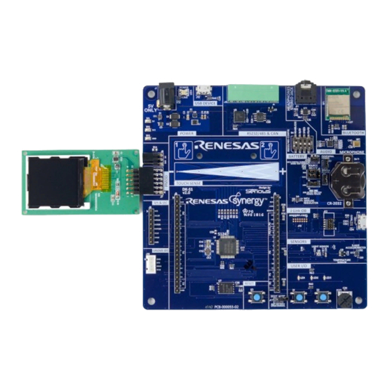
Development Kit DK-S124
v2.0
Renesas Synergy
All information contained in these materials, including products and product specifications,
represents information on the product at the time of publication and is subject to change by
Renesas Electronics Corp. without notice. Please review the latest information published by
Renesas Electronics Corp. through various means, including the Renesas Electronics Corp.
website (http://www.renesas.com).
www.renesas.com
User's Manual: Hardware
TM
Platform
Rev.1.00 Jun 2016
Advertisement
Table of Contents

Related Manuals for Renesas DK-S124


Summary of Contents for Renesas DK-S124
- Page 1 All information contained in these materials, including products and product specifications, represents information on the product at the time of publication and is subject to change by Renesas Electronics Corp. without notice. Please review the latest information published by Renesas Electronics Corp. through various means, including the Renesas Electronics Corp.
- Page 2 Renesas Electronics products are not subject to radiation resistance design. Please be sure to implement safety measures to guard them against the possibility of physical injury, and injury or damage caused by fire in the event of the failure of a Renesas Electronics product, such as safety design for hardware and software including but not limited to redundancy, fire control and malfunction prevention, appropriate treatment for aging degradation or any other appropriate measures.
- Page 3 Precautions This Renesas Synergy Development Kit is only intended for use in a laboratory environment under ambient temperature and humidity conditions. A safe separation distance should be used between this and any sensitive equipment. Its use outside the laboratory, classroom, study area or similar such area invalidates conformity with the protection requirements of the Electromagnetic Compatibility Directive and could lead to prosecution.
-
Page 4: Table Of Contents
SPI&I2C Interface ......... 31 Resources ..........10 7.1.11 PMOD Interface ........31 Chapter 2 Getting Started ........11 Human-Machine Interface....34 Powering the DK-S124 ......11 7.2.1 User Touch Buttons ......34 See the Demo ........12 7.2.2 User Touch Slider ......... 34 Chapter 3 Power Supplies ........ -
Page 5: Chapter 1 Overview
DK-S124 is primarily intended for software and hardware developers to develop firmware, experiment, and evaluate the I/O features of the S124 on the DK-S124 prior to development of their own customized hardware. The DK-S124 contains several communications ports, including Bluetooth Low Energy, CAN, RS-232/RS-485, SPI, I2C, and USB Device. -
Page 6: In The Box
SPI and/or I2C external communications interface devices for demonstrating operation of these interfaces 1.3 Environmental Characteristics The DKS124 is not designed as a production unit to be used direction in OEM equipment. Contact Renesas for a list of hardware design partners who can develop and deliver -productionready- platforms based on the ingredients used in the DK-S124 kit. -
Page 7: Physical Characteristics
Specification Minimum Typical Maximum Unit Storage Temperature Operating Temperature Humidity (Non-condensing) 1.4 Physical Characteristics The outer dimensions of the DK-S124 are approximately mm. Weight of the unit is 133.3 133.2 15.3 approximately 86 grams. R12UM0006EU0100 Rev.1.00 Page 7 of 40... -
Page 8: Block Diagram
DK-S124 User’s Manual Overview 1.5 Block diagram Figure 2: Block Diagram: Main Board RS-232 Head- Ambient RS-485 phones Sounds Bluetooth Device or Amp Device Power Jack RS-232 Stereo DC-DC RS-485 Out, Conv. Device Mic In Bluetooth Config./ J-Link Monitor Battery... -
Page 9: Hardware Features
DK-S124 User’s Manual Overview 1.6 Hardware features 1.6.1 Main Board 1.6.1.1 MCU and Board Memory • Synergy S1 MCU o 32-MHz ARM Cortex™-M0+ core o 16 kB on-chip SRAM o 64 or 128-KB on-chip code flash memory o 4-KB on-chip data flash memory o For additional peripherals, features, and configurations availability, see the S124 User’s Manual: Microcontrollers... -
Page 10: Programming And Debug Features
Provides all support circuitry to convert serial data to displayed data 1.7 Usage Models The DK-S124 is designed as a hardware design kit platform as well as software development platform for OEM applications requiring some Human Machine Interface (HMI) and communications capabilities. The platform has some direct machine-control-support GPIO available through the PMOD and Seeed Grove ports, although the platform may also be used in conjunction with an OEM’s intelligent I/O and power subsystem, possibly... -
Page 11: Chapter 2 Getting Started
Getting Started The DK-S124 includes the Main Board assembled with bumper feet and an acrylic cover over the touch region, a PMOD serial LCD daughter card, a 3-foot (91-cm) USB Type A to Micro-B adapter cable, and a Quick Start Guide. -
Page 12: See The Demo
USB port, both LED4 LEDs are lit on J-Link MCU commands making LED4 appear orange. LED4 is located in the box labeled “POWER” on the DK-S124. LED4 is not powered by the coin cell with jumpers properly installed. -
Page 13: Chapter 3 Power Supplies
The DK-S124 is delivered preloaded with a demonstration program. The demonstration program shows several features of the DK-S124 and source code is available as a programming example for developers. See the Quick Start Guide delivered with the DK-S124 for details of use of and expected board behavior when running the demonstration program. -
Page 14: V Main Power Subsystem
This switcher, using a tiny inductor, creates 3.3 V at up to 2 A to the DK-S124. It can operate with +5-V rail voltage between about 5.8 V and about 2 V. The variant of the switcher shown is internally set for FB pin voltage of 3.3 V. -
Page 15: Power Budgets
DK-S124 User’s Manual Power Supplies Therefore, LED4 orange indicates both J-Link MCU activity and 3.3-V Main Power available, and LED4 green indicates 3.3-V Main Power available, implying the availability of either 5 V from barrel jack J1 or 5 V from the J- Link USB connector J14. -
Page 16: Microcontroller Current
DK-S124 User’s Manual Power Supplies 4. USB current does NOT include additional load on MCU_VCC line during USB operations. Typical values estimated for 10% communications, Max for 4x datasheet typical at 100% communications (no max on datasheet). 5. CAN typical 10% receive, 10% transmit, 80% standby. Max 100% transmit. Power taken from +5-V bus and internal chip regulation “enhanced”... -
Page 17: Chapter 4Components
PC or other USB Host jack. The connector on the second is Micro-B for insertion into either the J10 USB Device or the J14 J-Link jack on the DK-S124 main board. If both connections are needed simultaneously, a second cable will be needed. -
Page 18: Cr2032 Lithium Battery
4.6 External Power Supply The DK-S124 is intended to be used with the USB cable providing power, but a barrel jack is also provided on the main board for an external 5V source. A wall-mounted AC-to-DC power converter may be used with the DK-S124, plugged into J1 near the upper left corner of the main board. -
Page 19: Chapter 5 Board Layout
DK-S124 User’s Manual Board Layout Chapter 5 Board Layout Figure 7: Main Board Components, Top Side R12UM0006EU0100 Rev.1.00 Page 19 of 40 Jun 8, 2016... - Page 20 DK-S124 User’s Manual Board Layout Figure 8: Main Board Components, Bottom Side R12UM0006EU0100 Rev.1.00 Page 20 of 40 Jun 8, 2016...
-
Page 21: Chapter 6 Configuration
DK-S124 User’s Manual Connectivity Chapter 6 Configuration The DK-S124 has the following configuration options: • Jumper J17 for S124 MCU boot configuration • Jumpers J2, J3, J18, J19, J20, for battery/5 V power source selection • DIP switch S4 for RS-232/485 transceiver configuration 6.1 MCU Boot Configuration Jumper... -
Page 22: Rs-232/485 Transceiver Configuration
DK-S124 User’s Manual Connectivity be chosen to have less than a 0.1-V drop at maximum expected load. With a resistor installed at R4, the jumper may be removed, since the connection will always be made. J19 will normally have a jumper installed across its pins. Removing the jumper will remove power from the light sensor, the temperature sensor, and sensor portions of the 3-axis accelerometer. - Page 23 DK-S124 User’s Manual Connectivity Table 4: RS-232/485 Configuration DIP Switches MCU Control TX/RX Status P0_2 P0_3 P4_10 J4-7 J4-8 Max Speed 232 SLW HALF RS_DEN RS_ON RXD0 (Mbps) Mode TXD0# TXD0 TXD0# TXD0 422/485 TXD0# TXD0 OFF/ 0.460/0.115 TXD0# TXD0 TXD0# TXD0 0.460...
-
Page 24: Chapter 7 Connectivity
The RS-232/485 and CAN connector header connects the ISL41387 RS-232/485 transceiver and the IFX1050 CAN transceiver to the mating screw-terminal-block adapter supplied with the DK-S124 kit. The S124 MCU interfaces with the ISL41387 RS-232/485 transceiver are shown in Table 7. - Page 25 DK-S124 User’s Manual Connectivity Table 6: RS-232/485 Transceiver ISL41387 RS-232/485 Transceiver S124 Microcontroller Logical Description Pin(s) Function Name(s) Receive Channel A P4_10 P4_10/RXD0 (NOT CONNECTED) No Connect Not Applicable Receive Enable, logically compared to RXEN No Connect Not Applicable RXEN# (Controlled by S4 FD/HD switch)
-
Page 26: Stereo Headphone Jack
DK-S124 User’s Manual Connectivity Table 8: RS-232/485 and CAN connector (J4) RS-232/485 and CAN Connector Transceiver Logical Description Pin(s) Function Name(s) CANH, CAN high CANH IFX1050, High line I/O CANL, CAN low CANL IFX1050, Low line I/O Not Connected No Connect... -
Page 27: S124 Programming And Debug
RESET# 7.1.7 J-Link JTAG Programming and Debug The Tag-Connect 14-pin connection pattern, without retainer clip holes, is a JTAG programming interface to the Renesas RX621 J-Link On-Board MCU. A Tag-Connect 14-pin adapter cable will properly mate with this pattern during programming. A friction clip may be needed to hold the cable’s spring-pin-connector... -
Page 28: Shield-Style Header Connection
DK-S124 User’s Manual Connectivity Table 12: J-Link JTAG Programming and Debug connector (J15) S124 Programming and Debug Connector J-Link OB Microcontroller Logical Description Pin(s) Function Name(s) JTCK, JTAG test clock signal (Circuit Ground) JTRST, JTGA test reset signal TRST JTEMLE, on-chip emulator enable... - Page 29 DK-S124 User’s Manual Connectivity Shield-Style Header Connectors S124 Microcontroller Logical Description Pin(s) Function Name(s) SPI communications for Bluetooth module, J5-8 P1_0 P1_0/MISOA serial flash memory, SPI&I2C connector SPI communications for Bluetooth module, J5-9 P1_1 P1_1/MOSIA serial flash memory, SPI&I2C connector...
-
Page 30: Seeed Grove I2C Interface
DK-S124 User’s Manual Connectivity Shield-Style Header Connectors S124 Microcontroller Logical Description Pin(s) Function Name(s) J6-13 PMOD interface, J7-10 (firmware defined) P4_3 (currently unassigned) J6-14 PMOD configurable interface P4_8 P4_8/RXD9 J6-15 PMOD configurable interface P4_9 P4_9/TXD9 J6-16 RS-232/485 received signal from ISL41387... -
Page 31: Spi&I2C Interface
DK-S124 User’s Manual Connectivity 7.1.10 SPI&I2C Interface The SPI&I2C interface connector is an 8-pin 2.54-mm-pitch single-column header with pin connections labelled on the PCB overlay. Table 15: SPI&I2C connector (J9) SPI&I2C Connector S124 Microcontroller Logical Description Pin(s) Function Name(s) +3V3 power bus (Config. - Page 32 DK-S124 User’s Manual Connectivity Table 16: PMOD connector (J7), Type 1 PMOD Connector, Type 2A (GPIO) S124 Microcontroller Logical Description Pin(s) Function Name(s) (Not connected) (Not connected) (Not connected) (Not connected) (Not connected) (Not connected) (Discrete firmware controlled PMOD input/output 1 (IO1)
- Page 33 1 into J7 pin 1. Firmware must properly configure all applicable pins. Always check the jumper position prior to inserting a PMOD. Applying 5 V to a 3.3-V PMOD may damage the PMOD and potentially the DK-S124. The power to this port is not fuse protected.
-
Page 34: Human-Machine Interface
DK-S124 User’s Manual Connectivity PMOD Connector, Type 4A (expanded UART) S124 Microcontroller Logical Description Pin(s) Function Name(s) (Circuit Ground) PMOD VCC, PMODA_PWR, configurable for (Depends on configuration) +5V or VPER (+3.3V) PMOD interrupt (INT) signal P1_4 P1_4/IRQ1 (Discrete firmware controlled... -
Page 35: User Push-Button Switches
DK-S124 User’s Manual Connectivity User Touch Slider S124 Microcontroller Designator Description Logical Pin(s) Function Name(s) TSL1-3 User capacitive slider segment 3 (center) P5_0 P5_0/TS27 TSL1-4 User capacitive slider segment 2 (right-center) P0_15 P0_15/TS28 TSL1-5 User capacitive slider segment 1 (rightmost) -
Page 36: User Potentiometer
DK-S124 User’s Manual Connectivity 7.2.5 User Potentiometer Immediately to the right of the user push button switches is one 10-kΩ thumbwheel potentiometer with its voltage tap fed to MCU’s ADC. Table 23: User Potentiometer User Potentiometer S124 Microcontroller Logical Designator... -
Page 37: C-Max Cmm-9301-V4.4
7.3.6 Bosch BMA250E Bosch BMA250E (U13) is a SPI or I2C (used on DK-S124) interface 3-axis accelerometer with ranges from +/- 2g to +/-16g selectable, low pass filtering selectable, a sample FIFO, extremely low power operating, and several modes to further reduce power. This chip provides two separate power buses, VDD for analog and internal sampling processes, and VDDIO for serial interface support. - Page 38 DK-S124 User’s Manual Connectivity supplied from the +3V3MCU bus, and the VDD power is supplied from the VSNS bus. This device has an I2C address of 0011000b (address byte 0x30 to OR with write bit). Table 27: 3-Axis Accelerometer (U13)
-
Page 39: Chapter 8 Glossary
DK-S124 User’s Manual Glossary Chapter 8 Glossary 8.1 Abbreviations and Acronyms ampere Inter-Integrated Circuit Serial Comms Bus Integrated Circuit Alternating Current Accel. Acceleration Input / Output Analog-to-Digital Converter IEEE Institute of Electrical and Electronics Engineers Amplifier Internet of Things Application Programming Interface... -
Page 40: Port Numbering
Farad 8.2 Port Numbering Renesas datasheets for MCUs generally refer to ports with numbers like “P001”, “P110”, and similar. This document generally refers to these ports as “P0_1” and “P1_10” respectively to add clarity. Port 5 bit 15 would be referred to in the datasheet as “P515”, in this manual as “P5_15”. The two forms should be considered identical in meaning. - Page 41 (WEEE), CE, UL, restricted substances (ROHS), FCC, FEE, and electromagnetic compatibility regulations. Renesas or its affiliates shall in no event be liable for any loss of profit, loss of data, loss of contract, loss of business, damage to reputation or goodwill, any economic loss, any reprogramming or recall costs (whether the foregoing...
- Page 42 Development Kit DK-S124 v2.0 User’s Manual: Hardware Publication Date: Rev.1.00 Jun 8, 2016 Published by: Renesas Electronics Corporation...
- Page 43 SALES OFFICES Refer to "http://www.renesas.com/" for the latest and detailed information. Renesas Electronics America Inc. 2801 Scott Boulevard Santa Clara, CA 95050-2549, U.S.A. Tel: +1-408-588-6000, Fax: +1-408-588-6130 Renesas Electronics Canada Limited 9251 Yonge Street, Suite 8309 Richmond Hill, Ontario Canada L4C 9T3...
- Page 44 Development Kit DK-S124 v2.0 User’s Manual: Hardware R12UM0006EU0100...
- Page 45 Mouser Electronics Authorized Distributor Click to View Pricing, Inventory, Delivery & Lifecycle Information: Renesas Electronics YSDKS124S20...
Need help?
Do you have a question about the DK-S124 and is the answer not in the manual?
Questions and answers