Renesas Synergy DK-S7G2 User Manual
Hide thumbs
Also See for Synergy DK-S7G2:
- User manual (74 pages) ,
- Quick start manual (16 pages) ,
- Quick start manual (5 pages)
Table of Contents
Advertisement
Quick Links
Download this manual
See also:
User Manual
Development Kit S7G2 (DK-S7G2)
Renesas Synergy™ Platform
Synergy Tools & Kits
Kits: DK-S7G2 v4.1
All information contained in these materials, including products and product specifications, represents
information on the product at the time of publication and is subject to change by Renesas Electronics
Corp. without notice. Please review the latest information published by Renesas Electronics Corp.
through various means, including the Renesas Electronics Corp. website (http://www.renesas.com).
www.renesas.com
User's Manual
Rev.1.00 Apr 2019
Advertisement
Table of Contents

Related Manuals for Renesas Synergy DK-S7G2


Summary of Contents for Renesas Synergy DK-S7G2
- Page 1 All information contained in these materials, including products and product specifications, represents information on the product at the time of publication and is subject to change by Renesas Electronics Corp. without notice. Please review the latest information published by Renesas Electronics Corp.
- Page 2 Renesas Electronics disclaims any and all liability for any damages or losses incurred by you or any third parties arising from the use of any Renesas Electronics product that is inconsistent with any Renesas Electronics data sheet, user’s manual or other Renesas Electronics document.
- Page 3 (WEEE), CE, UL, restricted substances (ROHS), FCC, FEE, and electromagnetic compatibility regulations. Renesas or its affiliates shall in no event be liable for any loss of profit, loss of data, loss of contract, loss of business, damage to reputation or goodwill, any...
-
Page 4: Table Of Contents
User’s Manual Renesas Synergy™ Platform Development Kit S7G2 (DK-S7G2) v4.1 Contents Overview ..........................2 Kit Contents ..........................5 Getting Started with Embedded Application Development on DK-S7G2 ........5 DK-S7G2 Hardware Details ..................... 6 Jumpers and DIP Switch Settings ......................6 4.1.1... -
Page 5: Overview
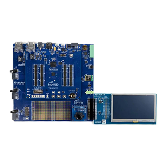
The kit includes breakout pin headers for direct access to the S7G2 microcontroller I/O pins. DIP configuration switches allow easy transition between different board configurations and ensure that the signal lines are always properly connected. • Renesas Synergy™ S7G2 Microcontroller Group R7FS7G27H2A01CBD 224-pin Ball Grid Array package ... - Page 6 Renesas Synergy™ Platform Development Kit S7G2 (DK-S7G2) v4.1 • Operating voltage External 5 V input through a 5 mm barrel jack connector supplies the on-board power regulator to power the Development Kit logic and interfaces. Button cell battery holder for on-board battery backup ...
- Page 7 Renesas Synergy™ Platform Development Kit S7G2 (DK-S7G2) v4.1 Figure 2. DK-S7G2 Bottom Side R12UM0035EU0100 Rev.1.00 Page 4 of 65 Apr.15.19...
-
Page 8: Kit Contents
Software Package and development tools are required to be installed on your computer. Step 1: Create My Renesas Account (if you do not have one already) You need a My Renesas account to download software, development tools, and application projects. Log in to or Sign up for a My Renesas account at www.update.renesas.com/SSO/login. -
Page 9: Dk-S7G2 Hardware Details
Renesas Synergy™ Platform Development Kit S7G2 (DK-S7G2) v4.1 4. DK-S7G2 Hardware Details 4.1 Jumpers and DIP Switch Settings 4.1.1 Default Board Configuration The Circuit Group for each jumper is the designation found in the board schematic. See Section 6, Electrical Schematics. -
Page 10: Hardware Layout
Renesas Synergy™ Platform Development Kit S7G2 (DK-S7G2) v4.1 5. Hardware Layout 5.1 System Block Diagram J-Link OB + Ethernet Power Jack USB Host Debug + Device ETM 20 Pin Debug USB FS USB HS ETHERC Interface Voltage/ SPI/ Power Current... -
Page 11: Power Requirements
Renesas Synergy™ Platform Development Kit S7G2 (DK-S7G2) v4.1 5.2 Power Requirements DK-S7G2 is designed for +5 V operation. A 5 V, 2.5 A wall-mounted power supply provides power through a barrel jack connector (J1) on DK-S7G2. The input power jack J1 supplies the main 5 V power to the system. -
Page 12: Measuring Current Consumption
Figure 4 for the location of J3 and J4. Figure 6. MCU Current Measurement Circuit 5.3 Main Components • Main MCU Renesas Synergy™ S7G2 MCU device, part number R7FS7G27C3A01CFB#AA0 (U1) • Main MCU • J-Link MCU Renesas Synergy™ S124 MCU device, part number R7FS124773A01CFM#AA0 (U42) •... - Page 13 Renesas Synergy™ Platform Development Kit S7G2 (DK-S7G2) v4.1 • DC-DC Buck-Boost Switching Regulator Renesas Intersil, part number ISL91107IINZ (U2) • Generates system 3.3 V from main 5 V input • LDO Regulator Texas Instruments, part number TLV70033DSE (U4) •...
-
Page 14: Connectivity And Settings
Renesas Synergy™ Platform Development Kit S7G2 (DK-S7G2) v4.1 5.4 Connectivity and Settings 5.4.1 Device USB The DEVICE USB Micro-B connection jack (J13) connects the Main MCU to an external USB Host, FS capable, allowing communications for testing and use of the Main MCU firmware. Power for the DK-S7G2 cannot be received from this connector. -
Page 15: Debug Usb
Renesas Synergy™ Platform Development Kit S7G2 (DK-S7G2) v4.1 5.4.3 Debug USB The J-Link OB USB Micro-B connection jack (J34) connects the S124 J-Link MCU to an external USB Host, FS capable, allowing re-programming and debugging of the Main MCU firmware. Power for the DK-S7G2 can NOT be received from this connector. -
Page 16: Jtag/Swd/Trace
Renesas Synergy™ Platform Development Kit S7G2 (DK-S7G2) v4.1 5.4.4 JTAG/SWD/TRACE ® A 20-pin Cortex Debug Connector is provided at J33. See Figure 8. A digital bus switch (U41) is provided to isolate the JTAG signals from the rest of the system. To enable the JTAG header (J33), set DIP Switch S7-2 to ON. -
Page 17: Switches
Renesas Synergy™ Platform Development Kit S7G2 (DK-S7G2) v4.1 LED15 Green PMOD A Enabled LED16 Green PMOD B Enabled LED17 Green QSPI Enabled LED18 Green CAN Enabled LED19 Green RS-232/485 Enabled LED20 Green SD Card Enabled LED21 Green SDRAM Enabled Figure 9. Reset Switch, User Switches, and User LEDs 5.4.6 Switches... -
Page 18: Pmod B
Renesas Synergy™ Platform Development Kit S7G2 (DK-S7G2) v4.1 Select using J20 INT (slave to master) P004 (IRQ9), U1-M11 RESET (master to slave) P911, U1-A7 Not Specified (GPIO) P912, U1-B7 Not Specified (GPIO) P913, U1-H8 Select using J20 Figure 10. PMOD A 5.4.8 PMOD B... -
Page 19: Pmod C
Renesas Synergy™ Platform Development Kit S7G2 (DK-S7G2) v4.1 Figure 11. PMOD B 5.4.9 PMOD C A 12-pin PMOD Type-2A connector is provided at PMOD C. The Main MCU acts as the SPI master, and the connected module acts as an SPI slave device. This interface may additionally be re-configured in firmware as several other PMOD types. -
Page 20: Pmod D
Renesas Synergy™ Platform Development Kit S7G2 (DK-S7G2) v4.1 5.4.10 PMOD D A 12-pin PMOD Type-2A connector is provided at PMOD D. The Main MCU acts as the SPI master, and the connected module acts as an SPI slave device. This interface may additionally be re-configured in firmware as several other PMOD types. -
Page 21: Ethernet 0
Renesas Synergy™ Platform Development Kit S7G2 (DK-S7G2) v4.1 5.4.11 Ethernet 0 The Ethernet 0 interface uses an RMII Ethernet Physical Layer Transceiver (PHY) (U23), connected to an RJ45 standard Ethernet connector (J16) with integrated magnetics and status indicators. The Ethernet clock is sourced from a precision 25 MHz clock crystal connected directly to the Ethernet PHY. -
Page 22: Ethernet 1
Renesas Synergy™ Platform Development Kit S7G2 (DK-S7G2) v4.1 5.4.12 Ethernet 1 The Ethernet 1 interface uses an RMII Ethernet Physical Layer Transceiver (PHY) (U27), connected to an RJ45 standard Ethernet connector (J17) with integrated magnetics and status indicators. The Ethernet clock is sourced from a precision 25 MHz clock crystal connected directly to the Ethernet PHY. -
Page 23: Rs232/485 Transceiver
Renesas Synergy™ Platform Development Kit S7G2 (DK-S7G2) v4.1 5.4.13 RS232/485 Transceiver DK-S7G2 includes an Intersil ISL41387 dual-protocol RS-232/485 Transceiver (U29) with loop-back mode and shutdown functions. The shutdown mode disables the receive and transmit outputs of the transceiver, disables the charge pump in RS-232 mode, and places the transceiver in low-current (35 μA) mode. -
Page 24: Can Transceiver
Renesas Synergy™ Platform Development Kit S7G2 (DK-S7G2) v4.1 5.4.14 CAN Transceiver The Infineon IFX1050GVIO CAN Transceiver (U31) supports transmission rates from 1 kbaud to 1 Mbaud. An On Semiconductor NUP2105 Bus Protector protects the CAN transceiver. The CAN transceiver is connected to CAN channel 0 on the S7G2 microcontroller and to connector J18. -
Page 25: Sdram
Renesas Synergy™ Platform Development Kit S7G2 (DK-S7G2) v4.1 5.4.16 SDRAM Included on DK-S7G2 is a Micron 256 Mb automotive grade SDR SDRAM (U8) in a 4M x 16 x 4 bank configuration (MT48LC16M16A2). Because the S7G2 MCU ports are highly multiplexed, some of the ports used for SDRAM signals are also used for PMOD C and PMOD D signals. -
Page 26: Sd Card Socket
Renesas Synergy™ Platform Development Kit S7G2 (DK-S7G2) v4.1 5.4.17 SD Card Socket Included on DK-S7G2 is an SD/MMC card socket (J12) with a four-bit data bus, plus card detect and write protect functions. The SD card socket is connected to channel 0 of the SD/MMC controller on the S7G2 MCU. -
Page 27: E.mmc
Renesas Synergy™ Platform Development Kit S7G2 (DK-S7G2) v4.1 5.4.18 e.MMC Included on DK-S7G2 is a Micron 4 GB e.MMC memory device with an eight-bit data bus (MTFC4GACAJCN-4M IT). The e.MMC memory is connected to channel 0 of the SD/MMC controller on the S7G2 MCU. -
Page 28: Camera Interface
Renesas Synergy™ Platform Development Kit S7G2 (DK-S7G2) v4.1 5.4.19 Camera Interface The DK-S7G2 Camera Module includes an Omnivision OV7670 image sensor with adjustable lens. The image sensor combines a VGA camera with an image processor and can be controlled through an I C bus interface connected to the Serial Communications Interface (SCI) peripheral on the S7G2 microcontroller. -
Page 29: Audio Jack
Renesas Synergy™ Platform Development Kit S7G2 (DK-S7G2) v4.1 5.4.20 Audio Jack DK-S7G2 contains an On Semiconductor 135 mW stereo headphone power amplifier (NCP2809BDMR2G). The output signals are generated by the Digital-to-Analog peripheral signals DA0 and DA1 on the S7G2 microcontroller. - Page 30 Renesas Synergy™ Platform Development Kit S7G2 (DK-S7G2) v4.1 Table 27. LCD Port Assignments LCD Signal LCD ZIF LCD ZIF DK-S7G2 Pi Filter Bridge Description Connector Connector Port Resistor (J28) Pin Pin Name LEDK LEDK LEDA LEDA +3.3 V DATA13 P907...
-
Page 31: External Lcd Connector
Renesas Synergy™ Platform Development Kit S7G2 (DK-S7G2) v4.1 Figure 21. On-board LCD Module 5.4.22 External LCD Connector In addition to the on-board LCD, DK-S7G2 provides an expansion connector for the use of an external LCD module. The External LCD interface supports a 16-bit LCD data bus, control signals, and I C bus to interface with a touch controller. - Page 32 Renesas Synergy™ Platform Development Kit S7G2 (DK-S7G2) v4.1 Table 28. External LCD Connector Port Assignments LCD Signal External LCD DK-S7G2 Port Description Connector (J29) Pin +3.3V LCD Present +3.3V DATA0 P804 DATA1 P803 DATA2 P802 DATA3 P606 DATA4 P607 DATA5...
-
Page 33: User Potentiometer
Renesas Synergy™ Platform Development Kit S7G2 (DK-S7G2) v4.1 5.4.23 User Potentiometer DK-S7G2 includes a 10 kΩ single-turn potentiometer (R16) connected to the Analog-to-Digital Converter (ADC) peripheral on the S7G2 MCU. This device is connected to P000 using the AN000 function assignment. -
Page 34: Configuration
Renesas Synergy™ Platform Development Kit S7G2 (DK-S7G2) v4.1 5.6 Configuration 5.6.1 Function select DIP switches Most pins of the Synergy S7G2 microcontroller support multiple functions and can therefore be connected to more than one device or connector on the DK-S7G2 board. To make it easy and safe to connect important functions, especially those with wide data bus connections, the DK-S7G2 provides banks of DIP switches S6, S7, S8, and S9. - Page 35 Renesas Synergy™ Platform Development Kit S7G2 (DK-S7G2) v4.1 Figure 26. Function Select DIP Switches S7 and S9 Figure 27. Function Selection R12UM0035EU0100 Rev.1.00 Page 32 of 65 Apr.15.19...
-
Page 36: Ethernet 0 Multiplexing
Renesas Synergy™ Platform Development Kit S7G2 (DK-S7G2) v4.1 5.6.2 Ethernet 0 Multiplexing Ethernet 0 is multiplexed with Audio Jack, SD Card, e.MMC, and Breakout Pin Headers. To enable Ethernet 0, set S6-2 to ON. The selection DIP switches for the SD Card and e.MMC do not matter when Ethernet 0 is enabled. -
Page 37: Ethernet 1 Multiplexing
Renesas Synergy™ Platform Development Kit S7G2 (DK-S7G2) v4.1 5.6.3 Ethernet 1 Multiplexing Ethernet 1 is multiplexed with the Camera Module and some ports on the Breakout Pin Headers. To enable Ethernet 1, set S6-3 to ON and S8-2 to OFF. This also enables the multiplexed ports that are routed to the Breakout Pin Headers. -
Page 38: Lcd Multiplexing
Renesas Synergy™ Platform Development Kit S7G2 (DK-S7G2) v4.1 5.6.4 LCD Multiplexing Ports used for the on-board LCD are shared with the external LCD, and some LCD ports are multiplexed with the e.MMC. These shared and multiplexed signals are always available at the Breakout Pin Headers. -
Page 39: Sdram Multiplexing
Renesas Synergy™ Platform Development Kit S7G2 (DK-S7G2) v4.1 5.6.5 SDRAM Multiplexing Ports used for the SDRAM are multiplexed with PMOD C, PMOD D, and some ports on the Breakout Pin Headers. To enable the SDRAM and disable the other multiplexed functions, set S9-2 to ON. -
Page 40: Electrical Schematics
Renesas Synergy™ Platform Development Kit S7G2 (DK-S7G2) v4.1 6. Electrical Schematics R12UM0035EU0100 Rev.1.00 Page 37 of 65 Apr.15.19... - Page 41 Renesas Synergy™ Platform Development Kit S7G2 (DK-S7G2) v4.1 R12UM0035EU0100 Rev.1.00 Page 38 of 65 Apr.15.19...
- Page 42 Renesas Synergy™ Platform Development Kit S7G2 (DK-S7G2) v4.1 R12UM0035EU0100 Rev.1.00 Page 39 of 65 Apr.15.19...
- Page 43 Renesas Synergy™ Platform Development Kit S7G2 (DK-S7G2) v4.1 R12UM0035EU0100 Rev.1.00 Page 40 of 65 Apr.15.19...
- Page 44 Renesas Synergy™ Platform Development Kit S7G2 (DK-S7G2) v4.1 R12UM0035EU0100 Rev.1.00 Page 41 of 65 Apr.15.19...
- Page 45 Renesas Synergy™ Platform Development Kit S7G2 (DK-S7G2) v4.1 R12UM0035EU0100 Rev.1.00 Page 42 of 65 Apr.15.19...
- Page 46 Renesas Synergy™ Platform Development Kit S7G2 (DK-S7G2) v4.1 R12UM0035EU0100 Rev.1.00 Page 43 of 65 Apr.15.19...
- Page 47 Renesas Synergy™ Platform Development Kit S7G2 (DK-S7G2) v4.1 R12UM0035EU0100 Rev.1.00 Page 44 of 65 Apr.15.19...
- Page 48 Renesas Synergy™ Platform Development Kit S7G2 (DK-S7G2) v4.1 R12UM0035EU0100 Rev.1.00 Page 45 of 65 Apr.15.19...
- Page 49 Renesas Synergy™ Platform Development Kit S7G2 (DK-S7G2) v4.1 R12UM0035EU0100 Rev.1.00 Page 46 of 65 Apr.15.19...
- Page 50 Renesas Synergy™ Platform Development Kit S7G2 (DK-S7G2) v4.1 R12UM0035EU0100 Rev.1.00 Page 47 of 65 Apr.15.19...
- Page 51 Renesas Synergy™ Platform Development Kit S7G2 (DK-S7G2) v4.1 R12UM0035EU0100 Rev.1.00 Page 48 of 65 Apr.15.19...
- Page 52 Renesas Synergy™ Platform Development Kit S7G2 (DK-S7G2) v4.1 R12UM0035EU0100 Rev.1.00 Page 49 of 65 Apr.15.19...
- Page 53 Renesas Synergy™ Platform Development Kit S7G2 (DK-S7G2) v4.1 R12UM0035EU0100 Rev.1.00 Page 50 of 65 Apr.15.19...
- Page 54 Renesas Synergy™ Platform Development Kit S7G2 (DK-S7G2) v4.1 R12UM0035EU0100 Rev.1.00 Page 51 of 65 Apr.15.19...
- Page 55 Renesas Synergy™ Platform Development Kit S7G2 (DK-S7G2) v4.1 R12UM0035EU0100 Rev.1.00 Page 52 of 65 Apr.15.19...
- Page 56 Renesas Synergy™ Platform Development Kit S7G2 (DK-S7G2) v4.1 R12UM0035EU0100 Rev.1.00 Page 53 of 65 Apr.15.19...
- Page 57 Renesas Synergy™ Platform Development Kit S7G2 (DK-S7G2) v4.1 R12UM0035EU0100 Rev.1.00 Page 54 of 65 Apr.15.19...
- Page 58 Renesas Synergy™ Platform Development Kit S7G2 (DK-S7G2) v4.1 R12UM0035EU0100 Rev.1.00 Page 55 of 65 Apr.15.19...
- Page 59 Renesas Synergy™ Platform Development Kit S7G2 (DK-S7G2) v4.1 R12UM0035EU0100 Rev.1.00 Page 56 of 65 Apr.15.19...
- Page 60 Renesas Synergy™ Platform Development Kit S7G2 (DK-S7G2) v4.1 R12UM0035EU0100 Rev.1.00 Page 57 of 65 Apr.15.19...
- Page 61 Renesas Synergy™ Platform Development Kit S7G2 (DK-S7G2) v4.1 R12UM0035EU0100 Rev.1.00 Page 58 of 65 Apr.15.19...
- Page 62 Renesas Synergy™ Platform Development Kit S7G2 (DK-S7G2) v4.1 R12UM0035EU0100 Rev.1.00 Page 59 of 65 Apr.15.19...
- Page 63 Renesas Synergy™ Platform Development Kit S7G2 (DK-S7G2) v4.1 R12UM0035EU0100 Rev.1.00 Page 60 of 65 Apr.15.19...
- Page 64 Renesas Synergy™ Platform Development Kit S7G2 (DK-S7G2) v4.1 R12UM0035EU0100 Rev.1.00 Page 61 of 65 Apr.15.19...
-
Page 65: Mechanical Drawing
Renesas Synergy™ Platform Development Kit S7G2 (DK-S7G2) v4.1 7. Mechanical Drawing R12UM0035EU0100 Rev.1.00 Page 62 of 65 Apr.15.19... -
Page 66: Certifications
Renesas Synergy™ Platform Development Kit S7G2 (DK-S7G2) v4.1 8. Certifications FCC Compliance This device complies with part 15 of the FCC Rules. Operation is subject to the following two conditions: (1) This device may not cause harmful interference, and (2) this device must accept any interference received, including interference that may cause undesired operation. - Page 67 Renesas Synergy™ Platform Development Kit S7G2 (DK-S7G2) v4.1 Website and Support Visit the following vanity URLs to learn about key elements of the Synergy Platform, download components and related documentation, and get support. Synergy Software www.renesas.com/synergy/software Synergy Software Package www.renesas.com/synergy/ssp Software add-ons www.renesas.com/synergy/addons...
-
Page 68: Revision History
Renesas Synergy™ Platform Development Kit S7G2 (DK-S7G2) v4.1 Revision History Description Rev. Date Page Summary 1.00 Apr.15.19 First release document R12UM0035EU0100 Rev.1.00 Page 65 of 65 Apr.15.19... - Page 69 Development Kit S7G2 (DK-S7G2) User’s Manual Publication Date: Apr.15.19 Published by: Renesas Electronics Corporation...
- Page 70 Renesas Synergy™ Platform Development Kit S7G2 (DK-S7G2) R12UM0035EU0100...
Need help?
Do you have a question about the Synergy DK-S7G2 and is the answer not in the manual?
Questions and answers