
Related Manuals for Telit Wireless Solutions ELS62


Summary of Contents for Telit Wireless Solutions ELS62
- Page 1 ELS62 Hardware Interface Description 1VV0301851 - Rev. 1 v01.100a 2023-9-27 Released Confidential Technical Documentation...
-
Page 2: Table Of Contents
2.4 Conventions ..........................9 2.5 Terms and Conditions........................ 10 2.6 Disclaimer ............................ 10 2.7 Key Features at a Glance......................11 2.8 ELS62 System Overview ......................16 2.9 Circuit Concept ..........................17 Interface Characteristics ...................... 19 3.1 Application Interface ......................... 19 3.1.1... - Page 3 4.2 Power Up/Power Down Scenarios..................69 4.2.1 Turn on ELS62........................ 69 4.2.1.1 Connecting ELS62 BATT+ Lines ............... 69 4.2.1.2 Switch on ELS62 Using ON Signal ............70 4.2.1.3 Automatic Power On .................. 71 4.2.2 Restart ELS62 ......................... 72 4.2.2.1 Restart ELS62 via AT+CFUN Command ..........72 4.2.2.2...
- Page 4 6.1.1 IEC 62368-1 Classification..................109 6.2 SAR requirements specific to portable mobiles ..............112 6.3 Reference Equipment for Type Approval................113 6.4 Compliance with FCC Rules and Regulations for ELS62-W..........114 Document Information....................... 117 7.1 Revision History ........................117 7.2 Related Documents ........................120 7.3 Terms and Abbreviations .......................120 7.4 Safety Precaution Notes......................124...
-
Page 5: Tables
Table 33: Toxic or hazardous substances or elements with defined concentration limits......................109 Table 34: IEC 62368-1 Classification.....................110 Table 35: Antenna gain limits for FCC (for ELS62-W variant only) .........114 Table 36: List of parts and accessories..................126 Table 37: Molex sales contacts (subject to change) ..............127 Table 38: ELS62 label information ....................128... -
Page 6: Figures
Figure 33: Routing to application‘s RF connector - top view ............64 Figure 34: Routing detail ........................64 Figure 35: Schematic diagram of ELS62 sample application ............. 66 Figure 36: Sample level conversion circuit ..................67 Figure 37: Sample circuit for applying power using an external µC......... 69 Figure 38: ON circuit options ...................... - Page 7 Figure 48: EMI circuits.......................... 88 Figure 49: ELS62 – top and bottom views ..................91 Figure 50: Dimensions of ELS62 (all dimensions in mm) ............92 Figure 51: Land pattern (top view)....................93 Figure 52: Recommended design for 110µm thick stencil (top view)........94 Figure 53: Recommended design for 150µm thick stencil (top view)........
-
Page 8: Applicability Table
ELS62 Hardware Interface Description Applicability Table Table 1: Applicability table Products ELS62-W v01.100a ELS62-E v01.100a ELS62-I v01.100a ELS62-BR v01.100a ELS62-C v01.100a 1VV0301851 Rev. 1 Page 8 of 129 2023-9-27... -
Page 9: Introduction
Wherever necessary, a note is made to differentiate between the product variants. Audience This document is intended for system integrators that are using the ELS62 modules in their products. Contact Information, Support For technical support and general questions, e-mail: •... -
Page 10: Terms And Conditions
ELS62 Hardware Interface Description Terms and Conditions Refer to https://www.telit.com/hardware-terms-conditions/. Disclaimer THE MATERIAL IN THIS DOCUMENT IS FOR INFORMATIONAL PURPOSES ONLY. TELIT CIN- TERION RESERVES THE RIGHT TO MAKE CHANGES TO THE PRODUCTS DESCRIBED HEREIN. THE SPECIFICATIONS IN THIS DOCUMENT ARE SUBJECT TO CHANGE AT THE DISCRETION OF TELIT CINTERION WITHOUT PRIOR NOTICE. -
Page 11: Key Features At A Glance
ELS62 Hardware Interface Description Key Features at a Glance Table 2: Key Features Feature Implementation General Frequency bands ELS62-W GSM/GPRS/EDGE bands: 850 (BdV) / 900 (BdVIII) / 1800 (BdIII) / 1900 (BdII) LTE bands: 2100 (Bd1) / 1900 (Bd2) / 1800 (Bd3) / 2100 (Bd4) - Page 12 ELS62 Hardware Interface Description Table 2: Key Features Feature Implementation Output power Class 3 for LTE 2100, LTE FDD Bd1 (according to Class 3 for LTE 1900, LTE FDD Bd2 Release 99) Class 3 for LTE 1800, LTE FDD Bd3...
- Page 13 ELS62 Hardware Interface Description Table 2: Key Features Feature Implementation Software AT commands Hayes 3GPP TS 27.007, TS 27.005, Telit Cinterion Cinterion AT commands for compatibility ® SIM Application SAT letter classes b, c, e; with BIP Toolkit Audio Support for Voice over LTE (VoLTE), i.e. Voice Service via IMS (IP-based Multimedia Subsystem) and CSFB.
- Page 14 Evaluation kit (For ordering information see Section 8.1) Evaluation module ELS62 module soldered onto a dedicated PCB that can be connected to an adapter in order to be mounted onto the DSB75 or DSB-Mini. EVAL DSB Adapter EVAL DSB Adapter for mounting the ELS62 evaluation module to the DSB75 or DSB-Mini.
- Page 15 ELS62 Hardware Interface Description Table 2: Key Features Feature Implementation LGA DevKit LGA DevKit is designed as a generic development adapter for LGA modules. With the LGA DevKit, it is no longer necessary to connect the evaluation modules to an adapter for test and development purposes.
-
Page 16: Els62 System Overview
ELS62 Hardware Interface Description ELS62 System Overview Application Module GPIO interface GPIO interface GPIOs Status Digital Audio PCM/I2S Serial modem ASC0 Interface lines Serial modem ASC1 Interface lines SIMSWITCH SIM switch Fast shutdown Fast shutdown Tuner Antenna tuner Serial modem... -
Page 17: Circuit Concept
ELS62 Hardware Interface Description Circuit Concept Figure 2 Figure 3 show block diagrams of the ELS62 module and illustrate the major functional components: VBATT_BB LDOs SIM1 SIM1 LDOs SIM2 SIM2 CCIN1/2 CCIN BUCK Buck VDDLP GPIOs GPIOs Detect ALARM VBUS... -
Page 18: Figure 3: Els62 Rf Section Block Diagram
LNA6_MHB Duplexer TRX5 LNA4_MHB Duplexer TRX3 B4/B66 LNA5_MHB Duplexer TRX4 LNA3_MHB Duplexer TRX2 LNA2_MHB Duplexer TRX1 26MHz B34/39 LNA10_LMB TRX10 Co-layout TXLB2 LB_IN TXMHB1 HB_IN Figure 3: ELS62 RF section block diagram 1VV0301851 Rev. 1 Page 18 of 129 2023-9-27... -
Page 19: Interface Characteristics
ELS62 Hardware Interface Description Interface Characteristics ELS62 is equipped with an SMT application interface that connects to the external applica- tion. The SMT application interface incorporates the various application interfaces as well as the RF antenna interface. Application Interface 3.1.1... -
Page 20: Table 3: Pad Assignments
ELS62 Hardware Interface Description Table 3: Pad assignments Signal name Signal name Signal name GPIO22/FSC USB_DN GPIO21/DIN GPIO23/BCLK BATT+ rfu (dnu) rfu (dnu) GPIO5/LED rfu (dnu) GPIO17/TXD1 GPIO6 GPIO16/RXD1 GPIO7 GPIO18/RTS1 GPIO8/SIMSWITCH V180 GPIO19/CTS1 BATT+ RXD0 EMERG_RST CTS0 GPIO12 TXD0... - Page 21 Signal pads that are not used should not be connected to an external application. Please note that the reference voltages listed in Table 4 are the values measured directly on the ELS62 module. They do not apply to the accessories connected. 1VV0301851 Rev. 1 Page 21 of 129 2023-9-27...
-
Page 22: Figure 4: Els62 Bottom View: Pad Assignments
MICN (dnu) (dnu) (dnu) (dnu) CCVCC1 GPIO13/MCLK VMIC GPIO24 RTS0 VDDLP CCRST1 CCIN1 CCIO1 rfu (dnu) BATT+ V180 RXD0 CTS0 TXD0 rfu (dnu) /RING0 (dnu) Figure 4: ELS62 bottom view: Pad assignments 1VV0301851 Rev. 1 Page 22 of 129 2023-9-27... -
Page 23: Figure 5: Els62 Top View: Pad Assignments
(dnu) (dnu) (dnu) (dnu) CCVCC1 MICN GPIO13/MCLK VMIC CCIO1 CCIN1 CCRST1 VDDLP RTS0 GPIO rfu (dnu) TXD0 CTS0 RXD0 V180 BATT+ rfu (dnu) (dnu) RING0 Figure 5: ELS62 top view: Pad assignments 1VV0301851 Rev. 1 Page 23 of 129 2023-9-27... -
Page 24: Signal Properties
ELS62 Hardware Interface Description 3.1.2 Signal Properties Table 4: Signal properties Function Signal name IO Signal form and level Comment Power BATT+ GSM and LTE Lines of BATT+ and supply BATT+ GND must be con- max = 4.5V nected in parallel for min = 3.0V during Tx burst on... - Page 25 ELS62 Hardware Interface Description Table 4: Signal properties Function Signal name IO Signal form and level Comment Ignition max = 5V tolerant This signal switches the min = 1.3V module on, and is ris- max = 0.5V ing edge sensitive trig- High level pulse width >15ms...
- Page 26 ELS62 Hardware Interface Description Table 4: Signal properties Function Signal name IO Signal form and level Comment Serial RXD0 max = 0.25V at I = 1mA If unused keep lines interface min = 1.55V at I = -1mA open. CTS0 ASC0 max = 1.85V...
- Page 27 ELS62 Hardware Interface Description Table 4: Signal properties Function Signal name IO Signal form and level Comment 3V SIM CCRST1 max = 0.45V at I = 1mA Maximum cable length card CCRST2 min = 2.35V at I = -1mA or copper track to SIM interface max = 3.10V...
- Page 28 ELS62 Hardware Interface Description Table 4: Signal properties Function Signal name IO Signal form and level Comment GPIO GPIO1 - max = 0.25V If unused keep line interface GPIO3, min = 1.55V open. max = 1.85V GPIO5 - Please note that most GPIO8, max = 0.35V...
- Page 29 ELS62 Hardware Interface Description Table 4: Signal properties Function Signal name IO Signal form and level Comment Digital BCLK max = 0.25V at I=1mA If unused keep line audio min = 1.55V at I=-1mA open. interface max = 1.85V (DAI)
-
Page 30: Absolute Maximum Ratings
Current at VCORE in normal operation VDDLP in normal operation -0.15 Current at VDDLP in normal operation 1. Positive noted current means current sourcing from ELS62. Negative noted current means current sourcing towards ELS62. 1VV0301851 Rev. 1 Page 30 of 129... -
Page 31: Usb Interface
ELS62 Hardware Interface Description 3.1.3 USB Interface ELS62 supports a USB 2.0 High Speed (480Mbit/s) device interface that is Full Speed (12Mbit/ s) compliant. The USB interface is primarily intended for use as command and data inter- face and for downloading firmware. -
Page 32: Serial Interface Asc0
4. For an illustration of the interface line’s startup behavior see Figure ELS62 is designed for use as a DCE. Based on the conventions for DCE-DTE connections it communicates with the customer application (DTE) using the following signals: • Port TXD @ application sends data to the module’s TXD0 signal line •... -
Page 33: Figure 8: Asc0 Startup Behavior
ELS62 Hardware Interface Description Note 1: The ASC0 modem control lines DTR0, DCD0, DSR0 and RING0 are originally avail- able as GPIO lines. If configured as ASC0 lines, these GPIO lines are assigned as follows: GPIO1 --> DTR0, GPIO2 --> DCD0, GPIO3 --> DSR0 and GPIO24 --> RING0. -
Page 34: Serial Interface Asc1
3.1.5 Serial Interface ASC1 Four ELS62 GPIO lines can be configured as ASC1 interface signals to provide a 4-wire un- balanced, asynchronous interface ASC1 conforming to ITU-T V.24 protocol DCE signaling. The electrical characteristics do not comply with ITU-T V.28. The significant levels are 0V (for low data bit or active state) and 1.8V (for high data bit or inactive state). -
Page 35: Uicc/Sim/Usim Interface
To take advantage of this feature, an appropriate SIM card detect switch is required on the card holder. For example, this is true for the model supplied by Molex, which has been tested to operate with ELS62 and is part of the Telit Cinterion reference equipment submit- ted for type approval. See Section 8.1... -
Page 36: Table 6: Signals Of The Sim Interface (Smt Application Interface)
SIM card during operation. Also, no guarantee can be given for properly initializing any SIM card that the user inserts after having removed the SIM card during op- eration. In this case, the application must restart ELS62. The figure below shows a circuit to connect an external SIM card holder. -
Page 37: Enhanced Esd Protection For Sim Interface
ELS62 Hardware Interface Description The total cable length between the SMT application interface pads on ELS62 and the pads of the external SIM card holder must not exceed 100mm in order to meet the specifica- tions of 3GPP TS 51.010-1 and to satisfy the requirements of EMC compliance. -
Page 38: Digital Audio Interface (Dai)
ELS62 Hardware Interface Description 3.1.7 Digital Audio Interface (DAI) ELS62 supports a digital audio interface that can be employed either as pulse code modu- lation interface (see Section 3.1.7.1) or as inter IC sound interface (see Section 3.1.7.2). 3.1.7.1 Pulse Code Modulation Interface (PCM) Four ELS62 GPIO lines can be configured as pule code modulation interface (PCM). -
Page 39: Inter Ic Sound Interface (I S)
ELS62 Hardware Interface Description Figure 13 Figure 14 shows the PCM timing for the master mode available with ELS62. 125 µs BCLK DOUT Figure 13: Long frame PCM timing, 8kHz 62.5 µs BCLK DOUT Figure 14: Short frame PCM timing, 16kHz 3.1.7.2 Inter IC Sound Interface (I... -
Page 40: Solutions For The Digital Audio Interface
ELS62 Hardware Interface Description The table below lists the available pads at the module’s digital audio interface. Table 8: Overview of DAI/I S lines Signal name Input/Output Description DOUT S data from module to external codec. S data from external codec to module. -
Page 41: Analog Audio Interface
NAUregister[7]=0x006 3.1.8 Analog Audio Interface ELS62 has an analog audio interface with a balanced analog microphone input and a bal- anced analog earpiece output. A supply voltage and an analog ground connection are pro- vided at dedicated pads. 3.1.8.1 Microphone Inputs and Supply A regulated power supply for electric microphones is available at VMIC. -
Page 42: Figure 18: Differential Microphone Connection
ELS62 Hardware Interface Description easily led away. It is recommended to use an additional RC-filter for VMIC (for example 470 Ohm and 10µF as shown in Figure 17) if a high microphone gain is necessary. Figure 18: Differential microphone connection If the microphone lines are long, use the above configuration. -
Page 43: Loudspeaker Output
ELS62 Hardware Interface Description 3.1.8.2 Loudspeaker Output ELS62 provides a differential loudspeaker output EPP/EPN. If the output is used as line out- put, the application should provide a capacitor decoupled differential input to eliminate GSM humming. A single ended connection to a speaker or a line input is strongly not rec- ommended. -
Page 44: Electrical Characteristics Of The Voiceband Part
3.1.8.3 Electrical Characteristics of the Voiceband Part Setting Audio Parameters by AT Commands The input and output volume of audio modes for ELS62 can be adjusted according to the AT command parameter listed in the table below. Each audio mode is assigned a separate set of parameters. -
Page 45: Gpio Interface
ELS62 Hardware Interface Description 3.1.9 GPIO Interface ELS62 offers a GPIO interface with 19 GPIO lines. The GPIO lines are shared with other in- terfaces or functions: Status LED (see Section 3.1.10.1), ASC0 (see Section 3.1.4), ASC1 (see Section 3.1.5), DAI interface (see Section 3.1.7), and SIM Switch. -
Page 46: Figure 23: Gpio Startup Behavior
ELS62 Hardware Interface Description The following figure shows the startup behavior of the GPIO interface. Start up Power supply active Firmware Command Interface Reset State Interface Active Initialization Initialization VCORE V180 EMERG_RST GPIO1 GPIO2 GPIO3,5,8,11-13 GPIO7 GPIO16-18 GPIO19 GPIO20-23 Figure 23: GPIO startup behavior 1VV0301851 Rev. -
Page 47: Control Signals
ELS62 Hardware Interface Description 3.1.10 Control Signals 3.1.10.1 Status LED The GPIO5 interface line can be configured to drive a status LED that indicates different op- erating modes of the module (for GPIOs see Section 3.1.9). GPIO and LED functionality are mutually exclusive. -
Page 48: Host Wakeup
ELS62 Hardware Interface Description External power supply Power indication V180 4.7k VCORE Figure 25: Power indication circuit 3.1.10.3 Host Wakeup If no call, data or message transfer is in progress, the host may shut down its own USB in- terface to save power. If a call or other request (URC’s, messages) arrives, the host can be notified of these events and be woken up again by a state transition of the ASC0 interface‘s... -
Page 49: Figure 26: Fast Shutdown Timing
ELS62 Hardware Interface Description It is recommended to keep the FST_SHDN line low until the module has shut down. A low level of the V180 signal indicates that the module has entered the Power Down mode. No shutdown URCs will be issued with a fast shutdown. Thus, it is recommended to monitor the V180 line by the external application. -
Page 50: Rf Antenna Interface
The external antenna must be matched properly to achieve best performance regarding radiated power, modulation accuracy and harmonic suppression. Antenna matching net- works are not included on the ELS62 module and should be placed in the host application if the antenna does not have an impedance of 50 Ω... -
Page 51: Antenna Interface Specifications
ELS62 Hardware Interface Description 3.2.1 Antenna Interface Specifications. Table 14: RF Antenna interface GSM/LTE (at normal temperature and voltage range) Parameter Conditions Min. Typi- Max. Unit LTE connectivity Band 1, 2, 3, 4, 5, 7, 8, 20, 28, 34, 38, 39, 40, 41, 66... - Page 52 ELS62 Hardware Interface Description Table 14: RF Antenna interface GSM/LTE (at normal temperature and voltage range) Parameter Conditions Min. Typi- Max. Unit LTE 2100 Band 66 +20.3 +23.0 +25.7 GPRS coding schemes Class 12, CS1 to CS4 EGPRS Class 12, MCS1 to MCS9...
- Page 53 ELS62 Hardware Interface Description Table 14: RF Antenna interface GSM/LTE (at normal temperature and voltage range) Parameter Conditions Min. Typi- Max. Unit EDGE, 2 TX GSM 850 26.5 E-GSM 900 26.5 DCS 1800 25.5 PCS 1900 25.5 GPRS, 3 TX GSM 850 32.7...
- Page 54 ELS62 Hardware Interface Description Table 14: RF Antenna interface GSM/LTE (at normal temperature and voltage range) Parameter Conditions Min. Typi- Max. Unit EDGE, 2 TX GSM 850 26.5 E-GSM 900 26.5 DCS 1800 25.5 PCS 1900 25.5 GPRS, 3 TX GSM 850 32.7...
- Page 55 ELS62 Hardware Interface Description Table 14: RF Antenna interface GSM/LTE (at normal temperature and voltage range) Parameter Conditions Min. Typi- Max. Unit EDGE, 2 TX GSM 850 26.5 E-GSM 900 26.5 DCS 1800 25.5 PCS 1900 25.5 GPRS, 3 TX GSM 850 30.7...
- Page 56 ELS62 Hardware Interface Description Table 14: RF Antenna interface GSM/LTE (at normal temperature and voltage range) Parameter Conditions Min. Typi- Max. Unit EDGE, 2 TX GSM 850 26.5 E-GSM 900 26.5 DCS 1800 25.5 PCS 1900 25.5 GPRS, 3 TX GSM 850 28.7...
-
Page 57: Antenna Installation
The antenna is connected by soldering the antenna pad (ANT_MAIN) and its neighboring ground pads (GND) directly to the application’s PCB. The antenna pads are the antenna ref- erence points (ARP) for ELS62. All RF data specified throughout this document is related to the ARP. -
Page 58: Figure 27: Antenna Pads (Bottom View)
For type approval purposes, the use of a 50 coaxial antenna connector (U.FL-R-SMT) Ω might be necessary. In this case the U.FL-R-SMT connector should be placed as close as possible to ELS62‘s antenna pad. 1VV0301851 Rev. 1 Page 58 of 129 2023-9-27... -
Page 59: Rf Line Routing Design
ELS62 Hardware Interface Description 3.2.3 RF Line Routing Design 3.2.3.1 Line Arrangement Examples Several dedicated tools are available to calculate line arrangements for specific applica- tions and PCB materials - for example from http://www.polarinstruments.com/ (commer- cial software) or from https://www.awr.com/awr-software/options/tx-line https:// saturnpcb.com/saturn-pcb-toolkit/ (free software). -
Page 60: Figure 29: Micro-Stripline On 1.0Mm Standard Fr4 2-Layer Pcb - Example 1
ELS62 Hardware Interface Description Micro-Stripline This section gives two line arrangement examples for micro-stripline. • Micro-Stripline on 1.0mm Standard FR4 2-Layer PCB The following two figures show examples with different values for D1 (ground strip separation). Application board Ground line... -
Page 61: Figure 30: Micro-Stripline On 1.0Mm Standard Fr4 Pcb - Example 2
ELS62 Hardware Interface Description Application board Ground line Antenna line Ground line Figure 30: Micro-Stripline on 1.0mm Standard FR4 PCB - example 2 1VV0301851 Rev. 1 Page 61 of 129 2023-9-27... -
Page 62: Figure 31: Micro-Stripline On 1.5Mm Standard Fr4 Pcb - Example 1
ELS62 Hardware Interface Description • Micro-Stripline on 1.5mm Standard FR4 2-Layer PCB The following two figures show examples with different values for D1 (ground strip separation). Application board Ground line Antenna line Ground line Figure 31: Micro-Stripline on 1.5mm Standard FR4 PCB - example 1 1VV0301851 Rev. -
Page 63: Routing Example
The sample line width of 0.26mm and the spaces of 0.2mm are only recommended for an application with a PCB layer stack resembling the one of the ELS62 evaluation board, and with layer 5 cut clear (Bottom layer reference to Layer 4). For differ- ent layer stacks the line width will have to follow line routing rules, avoiding 90 degree cor- ners and using the shortest distance to the PCB’s coaxial antenna connector. -
Page 64: Figure 33: Routing To Application's Rf Connector - Top View
ELS62 Hardware Interface Description Figure 33: Routing to application‘s RF connector - top view Figure 34: Routing detail 1VV0301851 Rev. 1 Page 64 of 129 2023-9-27... -
Page 65: Sample Application
Sample Application Figure 35 shows a typical example of how to integrate an ELS62 module with an application. Usage of the various host interfaces depends on the desired features of the application. Because of the very low power consumption design, current flowing from any other source into the module circuit must be avoided, for example reverse current from high state ex- ternal control lines. -
Page 66: Figure 35: Schematic Diagram Of Els62 Sample Application
CCVCCx SIM1/ CCIOx SIM 2 CCRSTx CCCLKx 220nF All SIM components should be close to card holder. . Keep SIM wires low capacitive . Figure 35: Schematic diagram of ELS62 sample application 1VV0301851 Rev. 1 Page 66 of 129 2023-9-27... -
Page 67: Sample Level Conversion Circuit
ELS62 Hardware Interface Description 3.3.1 Sample Level Conversion Circuit Depending on the micro controller used by an external application ELS62‘s digital input and output lines (i.e., ASC0, ASC1 and GPIO lines) may require level conversion. The following Figure 36 shows a sample circuit with recommended level shifters for an external applica- tion‘s micro controller (with VLOGIC between 3.0V...3.6V). -
Page 68: Operating Characteristics
ELS62 Hardware Interface Description Operating Characteristics Operating Modes The table below briefly summarizes the various operating modes referred to throughout the document. Table 15: Overview of operating modes Mode Function Normal GSM / GPRS / Power saving set automatically when no call is in progress... -
Page 69: Power Up/Power Down Scenarios
ELS62 Hardware Interface Description Power Up/Power Down Scenarios In general, make sure not to turn on ELS62 while it is beyond the safety limits of voltage and temperature stated in Section 3.1.2.1. ELS62 immediately switches off after having started and detected these inappropriate conditions. In extreme cases this can cause permanent damage to the module. -
Page 70: Switch On Els62 Using On Signal
ELS62 Hardware Interface Description 4.2.1.2 Switch on ELS62 Using ON Signal After the operating voltage BATT+ is applied, ELS62 can be switched on by means of the ON signal. The ON signal is an edge triggered signal and allows the input voltage level up to 5V. The module starts into normal mode on detecting the rising edge of the ON signal. -
Page 71: Automatic Power On
ELS62 Hardware Interface Description Wait for 16ms 10.5s >6s >100ms VBATT+BB VDDLP >15ms 1.5ms V180 19ms VCORE EMERG_RST FST_SHDN ^SYSSTART RXD0 Figure 39: ON timing 4.2.1.3 Automatic Power On When an automatic power on function is required for an external module application, it is... -
Page 72: Restart Els62
Furthermore, the module may get damaged permanently under some unlikely circumstances. Therefore, this procedure is intended only for use in case of emergency, e.g. if ELS62 does not respond, if reset or shutdown via AT command fails. 1VV0301851 Rev. 1... -
Page 73: Signal States After Startup
ELS62 Hardware Interface Description 4.2.3 Signal States after Startup Table 16 lists the states each interface signal passes through during reset phase and the first firmware initialization. For further firmware startup initializations the values may differ because of different GPIO line configurations. -
Page 74: Turn Off Els62
Takes effect if ELS62 board temperature or voltage levels exceed a critical limit. 4.2.4.1 Switch off ELS62 Using AT Command The best and safest approach to powering down ELS62 is to issue the appropriate AT com- mand. This procedure lets ELS62 log off from the network and allows the software to enter into a secure state and safe data before disconnecting the power supply. -
Page 75: Automatic Shutdown
Section 4.2.5.3) The automatic shutdown procedure is equivalent to the power-down initiated with an AT command, i.e. ELS62 logs off from the network and the software enters a secure state avoiding loss of data. 4.2.5.1 Thermal Shutdown Each time the board temperature goes out of range (-20°C to +85°C) or back to normal, ELS62 instantly displays an alert (if enabled). -
Page 76: Undervoltage Shutdown
Table 17 for the as- sociated URCs. Table 17: Temperature dependent behavior Sending temperature alert (2min after ELS62 start-up, otherwise only if URC presenta- tion enabled) ^SCTM_B: 1 Board close to overtemperature limit. ^SCTM_B: -1 Board close to undertemperature limit. -
Page 77: Overvoltage Shutdown
This type of URC does not need to be activated by the user. It will be output automatically when fault conditions occur. Keep in mind that several ELS62 components are directly linked to BATT+ and, therefore, the supply voltage remains applied at major parts of ELS62. Especially the power amplifier linked to BATT+ is very sensitive to high voltage and might even be destroyed. -
Page 78: Power Saving While Attached To Gsm Networks
ELS62 Hardware Interface Description 4.3.1 Power Saving while Attached to GSM Networks The power saving possibilities while attached to a GSM network depend on the paging tim- ing cycle of the base station. The duration of a power saving interval can be calculated using the following formula: t = 4.615 ms (TDMA frame duration) * 51 (number of frames) * DRX... -
Page 79: Wake-Up Via Rts0
4.3.3 Wake-up via RTS0 RTS0 can be used to wake up ELS62 from SLEEP mode configured with AT^SPOW. Asser- tion of RTS0 (i.e., toggle from inactive high to active low) serves as wake up event, thus al- lowing an external application to almost immediately terminate power saving. After RTS0 assertion, the CTS0 line signals module wake up, i.e., readiness of the AT command inter-... -
Page 80: Power Supply
ELS62 Hardware Interface Description Power Supply ELS62 needs to be connected to a power supply at the SMT application interface - 2 lines BATT+, and GND. There are two separate voltage domains for BATT+: • BATT+ with a line mainly for the baseband power supply. -
Page 81: Table 19: Current Consumption Ratings
ELS62 Hardware Interface Description Table 19: Current consumption ratings Description Conditions Typical Unit rating OFF State Power Down 29.034 μA BATT+ supply current (i.e., sum of GSM SLEEP SLEEP @ DRX=9 USB disconnected 1.736 BATT+ State supply (UART deactivated) USB suspended 1.737... - Page 82 ELS62 Hardware Interface Description Table 19: Current consumption ratings Description Conditions Typical Unit rating Average GPRS Data transfer ROPR=4 BATT+ GSM900 supply GSM900; PCL=5; (max. reduction) (i.e., sum of current 1Tx/4Rx ROPR=0 BATT+ (no reduction) BATT+ GPRS Data transfer ROPR=4 GSM900;...
- Page 83 ELS62 Hardware Interface Description Table 19: Current consumption ratings Description Conditions Typical Unit rating EDGE Data transfer ROPR=4 GSM1800; PCL=0; (max. reduction) 2Tx/3Rx ROPR=0 (no reduction) EDGE Data transfer ROPR=4 GSM1800; PCL=0; (max. reduction) 4Tx/1Rx ROPR=0 (no reduction) Average GPRS Data transfer...
- Page 84 ELS62 Hardware Interface Description Table 19: Current consumption ratings Description Conditions Typical Unit rating GPRS Data transfer GSM850; PCL=5; 1Tx/ 2.90 1Rx @total mismatch GPRS Data transfer GSM900; PCL=5; 1Tx/ 3.10 1Rx @total mismatch GPRS Data transfer GSM1800; PCL=0; 1.55 1Tx/1Rx @total mismatch GPRS Data transfer GSM1900;...
-
Page 85: Minimizing Power Losses
When designing the power supply for your application please pay specific attention to pow- er losses. Ensure that the input voltage V never drops below 3.0V on the ELS62 board, BATT+ not even in a GSM transmit burst where current consumption can rise (for peak values see... -
Page 86: Measuring The Supply Voltage (Vbatt+)
RF interface. The duration of measuring ranges from 0.5 seconds in TALK/ DATA mode to 50 seconds when ELS62 is in IDLE mode or Limited Service (deregistered). The displayed voltage (in mV) is averaged over the last measuring period before the AT^SBV command was executed. -
Page 87: Electrostatic Discharge
Chapter Blocking against RF on Interface Lines There are no general blocking measures at LGA pads on ELS62-W to the external applica- tion. In the EMERG_RST, and SIM interface lines are serial resistors, or capacitors to GND, implemented to reduce the EMI and ESD problems. All other signal lines have no EMI mea- sures on the Module. -
Page 88: Table 22: Emi Measures On The Application Interface
ELS62 Hardware Interface Description The main power supply from an external application has to be a single voltage source and has to be expanded to two sub paths (star structure). Each voltage domain must be decou- pled by application with low ESR capacitors (>100μF MLCC X5R@ BATT+BB; >(100+47)μF MLCC X5R@ BATT+RF) as close as possible to LGA pads. - Page 89 ELS62 Hardware Interface Description Table 22: EMI measures on the application interface Signal name EMI measures Remark USB_DP It is not allowed to use any external ESD or EMI components on the signal lines USB_DN of this interface. RXD0 TXD0...
-
Page 90: Reliability Characteristics
ELS62 Hardware Interface Description Reliability Characteristics The test conditions stated below are an extract of the complete test specifications. Table 23: Summary of reliability test conditions Type of test Conditions Standard Vibration Frequency range: 10-20Hz; acceleration: DIN IEC 60068-2-6 Frequency range: 20-500Hz; accelera- tion: 15g Duration: 2h per axis;... -
Page 91: Mechanical Dimensions, Mounting And Packaging
ELS62 Hardware Interface Description Mechanical Dimensions, Mounting and Packaging Mechanical Dimensions of ELS62 Figure 49 shows the top and bottom view of ELS62 and provides an overview of the board's mechanical dimensions. For further details see Figure Top view Bottom view Figure 49: ELS62 –... -
Page 92: Figure 50: Dimensions Of Els62 (All Dimensions In Mm)
ELS62 Hardware Interface Description Figure 50: Dimensions of ELS62 (all dimensions in mm) 1VV0301851 Rev. 1 Page 92 of 129 2023-9-27... -
Page 93: Mounting Els62 Onto The Application Platform
ELS62 Hardware Interface Description Mounting ELS62 onto the Application Platform This section describes how to mount ELS62 onto the PCBs, including land pattern and sten- cil design, board-level characterization, soldering conditions, durability and mechanical handling. For more information on issues related to SMT module integration see also [5]. -
Page 94: Figure 52: Recommended Design For 110Μm Thick Stencil (Top View)
ELS62 Hardware Interface Description The central ground pads are primarily intended for stabilizing purposes, and may show some more voids than the application interface pads at the module's rim. This is accept- able, since they are electrically irrelevant. Figure 52: Recommended design for 110µm thick stencil (top view) -
Page 95: Board Level Characterization
ELS62 comprises components that are susceptible to damage induced by absorbed mois- ture. The Telit Cinterion ELS62 module complies with the latest revision of the IPC/JEDEC J-STD- 020 Standard for moisture sensitive surface mount devices and is classified as MSL 4. -
Page 96: Maximum Temperature And Duration
Warning: ELS62 is specified for one soldering cycle only. Once ELS62 is removed from the application, the module will very likely be destroyed and cannot be soldered onto another application. -
Page 97: Durability And Mechanical Handling
Durability and Mechanical Handling 5.2.4.1 Storage Conditions ELS62 modules, as delivered in tape and reel carriers, must be stored in sealed, moisture barrier anti-static bags. The conditions stated below are only valid for modules in their orig- inal packed state in weather protected, non-temperature-controlled storage locations. -
Page 98: Processing Life
Figure 55. The figure also shows the proper part orientation. The tape width is 44mm and the ELS62 modules are placed on the tape with a 32-mm pitch. The reels are 330mm in diameter with a core diameter of 100mm. -
Page 99: Orientation
ELS62 Hardware Interface Description 5.3.1.1 Orientation Figure 55: Carrier tape Reel direction of the Direction into SMD machine completely equipped tape View direction Pad 1 Pad 1 330mm 44mm Figure 56: Reel direction 1VV0301851 Rev. 1 Page 99 of 129... -
Page 100: Barcode Label
ELS62 Hardware Interface Description 5.3.1.2 Barcode Label A barcode label provides detailed information on the tape and its contents. It is attached to the reel. Barcode label Figure 57: Barcode label on tape reel Figure 58: Barcode label on tape reel - layout 1VV0301851 Rev. -
Page 101: Shipping Materials
ELS62 Hardware Interface Description 5.3.2 Shipping Materials ELS62 is distributed in tape and reel carriers. The tape and reel carriers used to distribute ELS62 are packed as described below, including the following required shipping materials: • Moisture barrier bag, including desiccant and humidity indicator card •... -
Page 102: Figure 60: Moisture Sensitivity Label
ELS62 Hardware Interface Description Figure 60: Moisture Sensitivity Label MBBs contain one or more desiccant pouches to absorb moisture that may be in the bag. The humidity indicator card described below should be used to determine whether the en- closed components have absorbed an excessive amount of moisture. -
Page 103: Transportation Box
ELS62 Hardware Interface Description The desiccant pouches should not be baked or reused once removed from the MBB. The humidity indicator card is a moisture indicator and is included in the MBB to show the approximate relative humidity level within the bag. Sample humidity cards are shown in Fig- 61. -
Page 104: Table 26: Vp Box Label Information
ELS62 Hardware Interface Description Figure 62: Sample of VP box label Table 26: VP Box label information Information Cinterion logo Product name Product ordering number Package ID number of VP box (format may vary depending on the product) Package ID barcode (Code 128) -
Page 105: Trays
ELS62 Hardware Interface Description 5.3.3 Trays If small module quantities are required, e.g., for test and evaluation purposes, ELS62 may be distributed in trays (for dimensions see Figure 63). The small quantity trays are an alter- native to the single-feed tape carriers normally used. However, the trays are not designed for machine processing. -
Page 106: Regulatory And Type Approval Information
Regulatory and Type Approval Information Directives and Standards ELS62 is designed to comply with the directives and standards listed below. It is the responsibility of the application manufacturer to ensure compliance of the final product with all provisions of the applicable directives and standards as well as with the technical specifications provided in the "ELS62 Hardware Interface Description”. -
Page 107: Table 29: Standards Of European Type Approval
ELS62 Hardware Interface Description Table 29: Standards of European type approval 3GPP TS 51.010-1 Digital cellular telecommunications system (Release 7); Mobile Sta- tion (MS) conformance specification; GCF-CC V3.84 Global Certification Forum - Certification Criteria ETSI EN 301 511 Global System for Mobile communications (GSM); Mobile Stations V12.5.1... -
Page 108: Table 30: Standards (Statutory Instruments) For Uk
ELS62 Hardware Interface Description Table 30: Standards (Statutory Instruments) for UK S.I. 2017 No. 1206 The Radio Equipment Regulations 2017 Chapter 1, clause 6- Table 31: Requirements of quality IEC 60068 Environmental testing EN 62311:2020 Assessment of electronic and electrical equipment related to... -
Page 109: Iec 62368-1 Classification
ELS62 Hardware Interface Description Table 33: Toxic or hazardous substances or elements with defined concentration limits 6.1.1 IEC 62368-1 Classification With respect to the safety requirements for audio/video, information and communication technology equipment defined by the hazard based product safety standard for ICT and AV equipment - i.e., IEC-62368-1 - Cinterion... -
Page 110: Table 34: Iec 62368-1 Classification
ELS62 Hardware Interface Description stand levels according to ES-1 / PS-1 also on all ports that are initially intended for signalling or audio, e.g., USB, RS-232, GPIOs, earphone and microphone interfaces. In addition, the external application (Customer Product) must be designed in a way to dis- ®... - Page 111 ELS62 Hardware Interface Description Table 34: IEC 62368-1 Classification Source of Energy Class Limits Thermal energy source TS-2 Under normal operating conditions, abnormal operating conditions or single fault conditions the temperature does not exceed +100°C on the metal surface (shielding)
-
Page 112: Sar Requirements Specific To Portable Mobiles
This requires the Specific Absorption Rate (SAR) of portable ELS62 based applica- tions to be evaluated and approved for compliance with national and/or international reg- ulations. -
Page 113: Reference Equipment For Type Approval
ELS62 Hardware Interface Description Reference Equipment for Type Approval The Telit Cinterion reference setup submitted to type approve ELS62 (including a special approval adapter for the DSB75) is shown in the following figure LTE / GSM Base Station Main Antenna... -
Page 114: Compliance With Fcc Rules And Regulations For Els62-W
Manufacturers of mobile or fixed devices incorporating ELS62-W modules are authorized to use the FCC Grants of the ELS62 modules for their own final products according to the conditions referenced in these documents. In this case, an FCC label of the module shall be visible from the outside, or the host device shall bear a second label stating "Contains FCC... - Page 115 ELS62 Hardware Interface Description ment generates, uses and can radiate radio frequency energy and, if not installed and used in accordance with the instructions, may cause harmful interference to radio communica- tions. However, there is no guarantee that interference will not occur in a particular instal- lation.
- Page 116 ELS62 Hardware Interface Description statement set out in §15.105 Information to the user or such similar statement and place it in a prominent location of host product manual. 1VV0301851 Rev. 1 Page 116 of 129 2023-9-27...
-
Page 117: Document Information
Updated antenna gain values in Table Added FCC KDB 996369 Statement. Preceding document: "Cinterion ELS62 Hardware Interface Description" Version 01.100a ® New document: "Cinterion ELS62 Hardware Interface Description" Version 01.100a, Rev. 0 ® Chapter What is new Added Table 28 and 6.4. - Page 118 Updated GPIO6 first start up configuration, FST_SHDN reset state, and FST_SHDN first start up configuration in Table 4.4.1 Updated values in Table Preceding document: "Cinterion ELS62 Hardware Interface Description" Version 00.804 ® New document: "Cinterion ELS62 Hardware Interface Description" Version 01.000 ® Chapter What is new Removed GPIO4.
- Page 119 Updated the Vibration test value. 5.3.1.2 Added Figure 5.3.2.2 Added Figure 62 Figure Preceding document: "Cinterion ELS62 Hardware Interface Description" Version 00.001c ® New document: "Cinterion ELS62 Hardware Interface Description" Version 00.026 ® Chapter What is new Updated key features. 3.1.1 Corrected issues in Pad assignment.
-
Page 120: Related Documents
ELS62 Hardware Interface Description Related Documents [1] ELS62 AT Command Set [2] ELS62 Release Note [3] Universal Serial Bus Specification Revision 2.0, April 27, 2000 [4] Application Note 40: Thermal Solutions [5] Application Note 48: SMT Module Integration [6] Differences between Selected Cinterion Modules, Hardware Migration Guide ®... - Page 121 ELS62 Hardware Interface Description Abbrevia- Description tion DCS 1800 Digital Cellular System, also referred to as PCN Discontinuous Reception Development Support Box Digital Signal Processor Data Set Ready Data Terminal Ready Discontinuous Transmission Enhanced Full Rate EGSM Enhanced GSM EIRP...
- Page 122 ELS62 Hardware Interface Description Abbrevia- Description tion Link Power Management Mbps Mbits per second Man Machine Interface Mobile Originated Mobile Station (GSM module), also referred to as TE MSISDN Mobile Station International ISDN number Mobile Terminated Negative Temperature Coefficient Original Equipment Manufacturer...
- Page 123 ELS62 Hardware Interface Description Abbrevia- Description tion Specific Absorption Rate Surface Accoustic Wave SELV Safety Extra Low Voltage Subscriber Identification Module Surface Mount Device Short Message Service Surface Mount Technology Serial Peripheral Interface SRAM Static Random Access Memory Terminal adapter (e.g. GSM module)
-
Page 124: Safety Precaution Notes
The following safety precautions must be observed during all phases of the operation, us- age, service or repair of any cellular terminal or mobile incorporating ELS62. Manufacturers of the cellular terminal are advised to convey the following safety information to users and operating personnel and to incorporate these guidelines into all manuals supplied with the product. - Page 125 ELS62 Hardware Interface Description IMPORTANT! Cellular terminals or mobiles operate using radio signals and cellular networks. Because of this, connection cannot be guaranteed at all times under all conditions. Therefore, you should never rely solely upon any wireless device for essential communications, for example emergency calls.
-
Page 126: Appendix
ELS62 Hardware Interface Description Appendix List of Parts and Accessories Table 36: List of parts and accessories Description Supplier Ordering information ELS62-W Telit Cinterion Standard module Telit Cinterion IMEI: Packaging unit (ordering) number: L30960- N7300-A110 Module label number: S30960-S7300-A110. ELS62-E... -
Page 127: Table 37: Molex Sales Contacts (Subject To Change)
ELS62 Hardware Interface Description Table 36: List of parts and accessories Description Supplier Ordering information DSB Mini Telit Cinterion Ordering number: L30960-N0030-A100 LGA DevKit Telit Cinterion LGA DevKit consists of Cinterion LGA DevKit SM Base PCB: ® Ordering number: L30960-N0111-A100... -
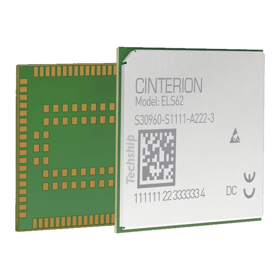
Page 128: Module Label Information
ELS62 Hardware Interface Description Module Label Information The label engraved on the top of ELS62 comprises the following information. Made in China N Model: ELS62-W FCC ID: QIPELS62-W S30960-S7300-A110 ANATEL: 12747-22-05015 11111111 222222 3 Figure 65: ELS62 Label Table 38:... - Page 129 © Telit 2023 All rights reserved. Technical Documentation...
Need help?
Do you have a question about the ELS62 and is the answer not in the manual?
Questions and answers