Table of Contents
Advertisement
Advertisement
Table of Contents

Related Manuals for Telit Wireless Solutions UE910 series


Summary of Contents for Telit Wireless Solutions UE910 series
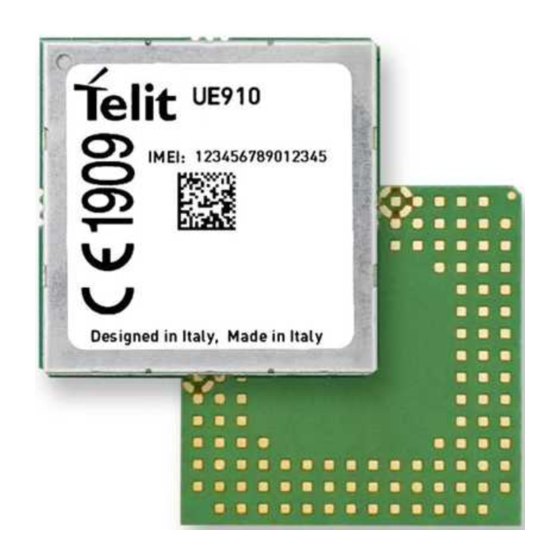
- Page 1 UE910 Hardware User Guide 1VV0301012 Rev.10.9 – 2016-12-16...
- Page 2 UE910 Hardware User Guide 1VV0301012 Rev.10.9 – 2016-12-16 Applicability Table PRODUCT UE910-EUR UE910-EUD UE910-NAR UE910-NAD UE910-GL Reproduction forbidden without Telit Communications S.p.A. written authorization - All Rights Reserved page 2 of 93...
- Page 3 DISCLAIMER The information contained in this document is the proprietary information of Telit Communications S.p.A. and its affiliates (“TELIT”). The contents are confidential and any disclosure to persons other than the officers, employees, agents or subcontractors of the owner or licensee of this document, without the prior written consent of Telit, is strictly prohibited. Telit makes every effort to ensure the quality of the information it makes available.
-
Page 4: Table Of Contents
Contents INTRODUCTION ................................. 6 1.1 S ....................................6 COPE 1.2 A ................................... 6 UDIENCE 1.3 C ............................6 ONTACT NFORMATION UPPORT 1.4 D ..............................7 OCUMENT RGANIZATION 1.5 T ................................8 ONVENTIONS 1.6 R ................................8 ELATED OCUMENTS 1.7 D ................................ - Page 5 USB HSIC ................................. 55 SERIAL PORTS ................................56 11.1 MODEM SERIAL PORT 1 (USIF0) ........................... 57 11.2 MODEM SERIAL PORT 2 (USIF1) ........................... 59 11.3 RS232 ..............................60 LEVEL TRANSLATION AUDIO SECTION OVERVIEW ............................ 62 12.1 A ..............................62 NALOG OICE NTERFACE 12.1.1 MIC connection ..............................
-
Page 6: Introduction
1 Introduction 1.1 Scope The aim of this document is the description of some hardware solutions useful for developing a product with the Telit UE910 module. 1.2 Audience This document is intended for Telit customers, who are integrators, about to implement their applications using our UE910 modules. -
Page 7: Document Organization
1.4 Document Organization This document contains the following chapters: Chapter 1: “Introduction” provides a scope for this document, target audience, contact and support information, and text conventions. Chapter 2: “Overview” provides an overview of the document. Chapter3: “UE910 Module Connections” deals with the pin out configuration and layout. Chapter 4: “Hardware Commands”... -
Page 8: Text Conventions
1.5 Text Conventions Danger – This information MUST be followed or catastrophic equipment failure or bodily injury may occur. Caution or Warning – Alerts the user to important points about integrating the module, if these points are not followed, the module and end user equipment may fail or malfunction. Tip or Information –... -
Page 9: Document History
1.7 Document History ISSUE#0 2012-09-07 Preliminary Version ISSUE#1 2013-04-10 Updated Chapters 5.2, 6.3, 6.4, 9, 11, 13.4, 15 ISSUE#2 2013-04-24 Updated Chapters 13.4, 15.2 ISSUE#3 2013-08-02 Updated Chapters 4, 5.1, 6.3, 12.4, 13.4, added Reel packaging chapter ISSUE#4 2013-08-30 Updated Chapters 3.1, 4.1, 4.2, 5.2, 7, 8.1, 10, 12.1 ISSUE#5 2013-12-20 Updated Chapters 1.4, 1.6, 3.1, updated schematics and flow charts;... -
Page 10: Overview
2 Overview The aim of this document is the description of some hardware solutions useful for developing a product with the Telit UE910 module. In this document all the basic functions of a mobile phone will be taken into account; for each one of them a proper hardware solution will be suggested and eventually the wrong solutions and common errors to be avoided will be evidenced. -
Page 11: Ue910 Module Connections
3 UE910 module connections 3.1 PIN-OUT Signal Function Type COMMENT USB HS 2.0 COMMUNICATION PORT USB_D+ USB differential Data (+) USB_D- USB differential Data (-) Power sense for the internal USB VUSB transceiver. Asynchronous Serial Port (USIF0) - Prog. / Data + HW Flow Control C103/TXD Serial data input from DTE CMOS 1.8V... - Page 12 Not available on UE910- EAR- Analog Audio Interface (EAR-) xxD/UE910-GL Not available on UE910- MIC+ Analog Audio Interface (MIC+) xxD/UE910-GL Not available on UE910- MIC- Analog Audio Interface (MIC-) xxD/UE910-GL Digital Voice Interface (DVI) DVI_WA0 Digital Audio Interface (WA0) CMOS 1.8V DVI_RX Digital Audio Interface (RX) CMOS 1.8V...
- Page 13 VBATT_PA Main power supply (Radio PA) Power VBATT_PA Main power supply (Radio PA) Power VBATT_PA Main power supply (Radio PA) Power Ground Power Ground Power Ground Power Ground Power Ground Power Ground Power Ground Power Ground Power Ground Power Ground Power Ground Power...
- Page 14 RESERVED RESERVED RESERVED RESERVED RESERVED RESERVED RESERVED RESERVED RESERVED RESERVED RESERVED RESERVED RESERVED RESERVED RESERVED RESERVED RESERVED RESERVED RESERVED RESERVED RESERVED RESERVED RESERVED RESERVED RESERVED RESERVED RESERVED RESERVED RESERVED RESERVED RESERVED RESERVED RESERVED RESERVED RESERVED RESERVED RESERVED RESERVED RESERVED RESERVED RESERVED RESERVED RESERVED...
- Page 15 RESERVED RESERVED RESERVED RESERVED RESERVED RESERVED RESERVED RESERVED RESERVED RESERVED RESERVED RESERVED RESERVED RESERVED RESERVED RESERVED RESERVED RESERVED RESERVED RESERVED RESERVED RESERVED RESERVED RESERVED RESERVED RESERVED RESERVED RESERVED RESERVED RESERVED RESERVED RESERVED WARNING: Reserved pins must not be connected. NOTE 1: The following table is listing the main Pinout differences between the UE910 variants Product Audio...
- Page 16 NOTE: If not used, almost all pins should be left disconnected. The only exceptions are the following pins: Signal Notes M1,M2,N1,N2,P1,P2 VBATT & VBATT_PA E1,G1,H1,J1,L1,A2,E2,F2,G2,H2, J2,K2,L2,R2,M3,N3,P3,R3,D4,M4, N4,P4,R4,N5,P5,R5,N6,P6,R6,P8, R8,P9,P10,R10,M12,B13,P13,E14 ON/OFF* HW_SHUTDOWN* USB_D+ If not used should be connected to a Test Point or an USB connector USB_D- If not used should be connected to a Test Point or an USB connector...
-
Page 17: Lga Pads Layout
3.1.1 LGA Pads Layout TOP VIEW VBATT_P VBATT_P ADC_IN1 VBATT VBATT_P VBATT_P SPK+ VBATT SIMVCC SPK - SIMIN MIC+ SIMIO MIC - SIMCLK DVI_RX SIMRST DVI_TX DVI_CLK GPIO_01 DVI_WA0 GPIO_02 GPIO_03 HSIC_US VAUX/PW GPIO_04 B_STRB RMON HSIC_US GPIO_06 ON_OFF* B_DATA HW_SHU VUSB GPIO_07... -
Page 18: Hardware Commands
4 Hardware Commands 4.1 Turning ON the UE910 To turn on the UE910 the pad ON_OFF* must be tied low for at least 5 seconds and then released. The maximum current that can be drained from the ON_OFF* pad is 0,1 mA. A simple circuit to do it is: NOTE: Don't use any pull up resistor on the ON_OFF* line, it is internally pulled up. - Page 19 A flow chart showing the proper turn on procedure is displayed below: Reproduction forbidden without Telit Communications S.p.A. written authorization - All Rights Reserved page 19 of 93...
- Page 20 “Modem ON Proc” START VBATT > 3.22V ? PWMON = ON ? ON_OFF* = LOW GOTO “HW SHUTDOWN Delay = 5 Sec unconditional” ON_OFF* = HIGH PWMON = ON ? Delay 1s GOTO “Start AT CMD.” “Modem ON Proc” Reproduction forbidden without Telit Communications S.p.A. written authorization - All Rights Reserved page 20 of 93...
- Page 21 A flow chart showing the AT commands managing procedure is displayed below: “Start AT CMD.” START DELAY 300msec Enter AT<CR> GOTO AT answer in “HW SHUTDOWN 1 sec ? unconditional” “Start AT CMD.” GOTO “Modem ON Proc.” Reproduction forbidden without Telit Communications S.p.A. written authorization - All Rights Reserved page 21 of 93...
- Page 22 NOTE: In order to avoid a back powering effect it is recommended to avoid having any HIGH logic level signal applied to the digital pins of the UE910 when the module is powered off or during an ON/OFF transition. For example: 1- Let's assume you need to drive the ON_OFF* pad with a totem pole output of a +3/5 V microcontroller (uP_OUT1): 2- Let's assume you need to drive the ON_OFF* pad directly with an ON/OFF button:...
- Page 23 WARNING It is recommended to set the ON_OFF* line LOW to power on the module only after VBATT is higher than 3.22V. In case this condition it is not satisfied you could use the HW_SHUTDOWN* line to recover it and then restart the power on activity using the ON_OFF * line.
- Page 24 After HW_SHUTSDOWN* is released you could again use the ON_OFF* line to power on the module. Reproduction forbidden without Telit Communications S.p.A. written authorization - All Rights Reserved page 24 of 93...
-
Page 25: Turning Off The Ue910
4.2 Turning OFF the UE910 Turning off of the device can be done in two ways: via AT command (see UE910 Software User Guide, AT#SHDN) by tying low pin ON_OFF* Either ways, the device issues a detach request to network informing that the device will not be reachable any more. - Page 26 The following flow chart shows the proper turn off procedure: Reproduction forbidden without Telit Communications S.p.A. written authorization - All Rights Reserved page 26 of 93...
- Page 27 Modem OFF Proc. START PWRMON=ON? OFF Mode ON_OFF* = LOW AT#SHDN Delay >= 3 Sec ON_OFF* = HIGH “Modem OFF Proc” PWMON = ON ? Looping for more than 15s ? GOTO “HW SHUTDOWN Unconditional” Reproduction forbidden without Telit Communications S.p.A. written authorization - All Rights Reserved page 27 of 93...
-
Page 28: Ue910 Unconditional Shutdown
4.3 UE910 Unconditional Shutdown The Unconditional Shutdown of the module could be activated using the HW_SHUTDOWN* line (pad R13). WARNING: The hardware unconditional Shutdown must not be used during normal operation of the device since it does not detach the device from the network. It shall be kept as an emergency exit procedure. - Page 29 A typical circuit is the following: example: 1- Let us assume you need to drive the HW_SHUTDOWN* pad with a totem pole output of a +3/5 V microcontroller (uP_OUT2): NOTE: In order to avoid a back powering effect it is recommended to avoid having any HIGH logic level signal applied to the digital pins of the UE910 when the module is powered off or during an ON/OFF transition.
- Page 30 “HW SHUTDOWN Unconditional” START HW_SHDN = LOW Delay 1s Delay 200ms Disconnect HW_SHDN = HIGH VBATT PWRMON = ON “HW SHUTDOWN Unconditional” Reproduction forbidden without Telit Communications S.p.A. written authorization - All Rights Reserved page 30 of 93...
-
Page 31: Power Supply
5 Power Supply The power supply circuitry and board layout are a very important part in the full product design and they strongly reflect on the product overall performances, hence read carefully the requirements and the guidelines that will follow for a proper design. 5.1 Power Supply Requirements The external power supply must be connected to VBATT &... -
Page 32: Power Consumption
5.2 Power Consumption UE910 Average Mode Mode description (mA) SWITCHED OFF Module supplied but Switched Off Switched Off 180 uA IDLE mode (WCDMA) AT+CFUN=1 12.2 Normal mode: full functionality of the module Full functionality with power saving; DRX7; AT+CFUN=5 Module registered on the network can receive incoming calls and SMS IDLE mode (GSM/EDGE) AT+CFUN=1... -
Page 33: General Design Rules
NOTE: The electrical design for the Power supply should be made ensuring it will be capable of a peak current output of at least 2 A. The UE910-EUx variants are supporting EDGE class 33; the NAx variants support EDGE class 5.3 General Design Rules The principal guidelines for the Power Supply Design embrace three different design steps: ... - Page 34 An example of linear regulator with 5V input is: 5.3.1.2 input Source Power Supply Design Guidelines The desired output for the power supply is 3.8V, hence due to the big difference between the input source and the desired output, a linear regulator is not suited and shall not be used. A switching power supply will be preferable because of its better efficiency especially with the 2A peak current load represented by the UE910.
- Page 35 Make sure the low ESR capacitor on the power supply output (usually a tantalum one) is rated at least 10V. For Car applications a spike protection diode should be inserted close to the power input, in order to clean the supply from spikes. ...
- Page 36 5.3.1.3 Battery Source Power Supply Design Guidelines The desired nominal output for the power supply is 3.8V and the maximum voltage allowed is 4.2V, hence a single 3.7V Li-Ion cell battery type is suited for supplying the power to the Telit UE910 module. WARNING: The three cells Ni/Cd or Ni/MH 3,6 V Nom.
-
Page 37: Thermal Design Guidelines
5.3.2 Thermal Design Guidelines The thermal design for the power supply heat sink should be done with the following specifications: Average current consumption during HSDPA transmission @PWR level max : 600 mA Average current during idle: 1.5 mA NOTE: The average consumption during transmissions depends on the power level at which the device is requested to transmit by the network. -
Page 38: Power Supply Pcb Layout Guidelines
5.3.3 Power Supply PCB layout Guidelines As seen on the electrical design guidelines the power supply shall have a low ESR capacitor on the output to cut the current peaks and a protection diode on the input to protect the supply from spikes and polarity inversion. - Page 39 The power supply input cables should be kept separate from noise sensitive lines such as microphone/earphone cables. The insertion of EMI filter on VBATT pins is suggested in those designs where antenna is placed close to battery or supply lines. A ferrite bead like Murata BLM18EG101TN1 or Taiyo Yuden P/N FBMH1608HM101 can be used for this purpose.
-
Page 40: Gsm/Wcdma Radio Section
6 GSM/WCDMA Radio Section 6.1 UE910 Product Variants The following table is listing the main differences between the UE910 variants: Product Supported 2G Bands Supported 3G bands UE910-EUR GSM 900, DCS1800 FDD B1, B8 UE910-EUD GSM 900, DCS1800 FDD B1, B8 UE910-NAR GSM 850, PCS 1900 FDD B2, B5... - Page 41 UE910-GL Band Power Class GSM 850, GSM 900 4 (2W) DCS 1800, PCS 1900 1 (1W) EDGE, 850/900 MHz E2 (0.5W) EDGE, 1800/1900 MHz Class E2 (0.4W) WCDMA FDD B1, B2, B4, B5, B8 Class 3 (0.25W) Reproduction forbidden without Telit Communications S.p.A. written authorization - All Rights Reserved page 41 of 93...
- Page 42 Reproduction forbidden without Telit Communications S.p.A. written authorization - All Rights Reserved page 42 of 93...
-
Page 43: Sensitivity
Sensitivity UE910-EUR and UE910-EUD Band Typical Note -109 dBm BER Class II <2.44% GSM 900 -110 dBm BER Class II <2.44% DCS1800 -111 dBm BER <0.1% WCDMA FDD B1 -110 dBm BER <0.1% WCDMA FDD B8 UE910-NAR and UE910-NAD Band Typical Note -109.5 dBm... - Page 44 (WCDMA) 80 MHz in WCDMA Band VIII 50 ohm Impedance > 33dBm(2 W) peak power in GSM Input power > 24dBm Average power in WCDMA ≤ 10:1 (limit to avoid permanent damage) VSWR absolute max ≤ 2:1 (limit to fulfil all regulatory requirements) VSWR recommended ANTENNA REQUIREMENTS (UE910-NAR and UE910-NAD) Depending by frequency band(s) provided by the network operator, the...
-
Page 45: Gsm/Wcdma - Pcb Line Guidelines
This transmission line shall fulfil the following requirements: ANTENNA LINE ON PCB REQUIREMENTS Characteristic Impedance 50 ohm Max Attenuation 0,3 dB Coupling with other signals shall be avoided Cold End (Ground Plane) of antenna shall be equipotential to the UE910 ground pins Furthermore if the device is developed for the US market and/or Canada market, it shall comply with the FCC and/or IC approval requirements: This device is to be used only for mobile and fixed application. - Page 46 The ground surrounding the antenna line on PCB has to be strictly connected to the main Ground Plane by means of via holes (once per 2mm at least), placed close to the ground edges facing line track; Place EM noisy devices as far as possible from UE910 antenna line; ...
-
Page 47: Pcb Guidelines In Case Of Fcc Certification
6.5 PCB Guidelines case certification In the case FCC certification is required for an application using UE910-NAx, according to FCC KDB 996369 for modular approval requirements, the transmission line has to be similar to that implemented on UE910 interface board and described in the following chapter. -
Page 48: Transmission Line Measurements
6.5.2 Transmission line measurements HP8753E VNA (Full-2-port calibration) has been used in this measurement session. A calibrated coaxial cable has been soldered at the pad corresponding to RF output; a SMA connector has been soldered to the board in order to characterize the losses of the transmission line including the connector itself. - Page 49 Line input impedance (in Smith Chart format, once the line has been terminated to 50 Ω load) is shown in the following figure: Insertion Loss of G-CPW line plus SMA connector is shown below: Reproduction forbidden without Telit Communications S.p.A. written authorization - All Rights Reserved page 49 of 93...
-
Page 50: Antenna - Installation Guidelines
6.6 Antenna - Installation Guidelines Install the antenna in a place covered by the GSM / WCDMA signal. If the device antenna is located farther than 20cm from the human body and there are no co-located transmitter then the Telit FCC/IC approvals can be re-used by the end product. -
Page 51: Logic Level Specifications
7 Logic level specifications The following table shows the logic level specifications used in the UE910 interface circuits: Absolute Maximum Ratings -Not Functional Parameter Input level on any digital pin (CMOS 1.8) with respect to ground -0.3V 2.1V Input level on any digital pin (CMOS 1.2) with respect to ground -0.3V 1.4V Operating Range - Interface levels (1.8V CMOS) -
Page 52: Unconditional Shutdown
7.1 Unconditional Shutdown Signal Function HW_SHUTDOWN* Unconditional Shutdown of the Module HW_SHUTDOWN* is used to unconditionally shutdown the UE910. Whenever this signal is pulled low, the UE910 is reset. When the device is reset it stops any operation. After the release of the line, the UE910 is unconditionally shut down, without doing any detach operation from the network where it is registered. -
Page 53: Usb Port
8 USB Port The UE910 includes one integrated universal serial bus (USB 2.0 HS) transceiver. 8.1 USB 2.0 HS This port is compliant with the USB 2.0 HS only. The USB FS is supported for AT interface and data communication. The following table is listing the available signals: Signal Function... -
Page 54: Spi Port
9 SPI port The UE910 Module is provided by one SPI interface. The SPI interface defines two handshake lines for flow control and mutual wake-up of the modem and the Application Processor: SRDY (slave ready) and MRDY (master ready). The AP has the master role, that is, it supplies the clock. The following table is listing the available signals: Signal Function... -
Page 55: Usb Hsic
10 USB HSIC The UE910 Module is provided by one USB HSIC interface. The USB HSIC (High Speed Inter Processor) Interface allows supporting the inter-processor communication between an application processor (AP) – the host, and the modem processor (CP) – the UE910. The following table is listing the available signals: Signal Direction... -
Page 56: Serial Ports
11 Serial Ports The UE910 module is provided with by 2 Asynchronous serial ports: MODEM SERIAL PORT 1 (Main) MODEM SERIAL PORT 2 (Auxiliary) Several configurations can be designed for the serial port on the OEM hardware, but the most common are: ... -
Page 57: Modem Serial Port 1 (Usif0)
11.1 MODEM SERIAL PORT 1 (USIF0) The serial port 1 on the UE910 is a +1.8V UART with all the 7 RS232 signals. It differs from the PC-RS232 in the signal polarity (RS232 is reversed) and levels. RS232 Signal UE910 Name Usage Pin #... - Page 58 The input line ON_OFF and RESET state can be treated as in picture below NOTE: According to V.24, some signal names are referred to the application side, therefore on the UE910 side these signal are on the opposite direction: TXD on the application side will be connected to the receive line (here named C103/TXD) RXD on the application side will be connected to the transmit line (here named C104/RXD) NOTE: For a minimum implementation, only the TXD, RXD lines can be connected, the other lines can...
-
Page 59: Modem Serial Port 2 (Usif1)
11.2 MODEM SERIAL PORT 2 (USIF1) The secondary serial port on the UE910 is a CMOS1.8V with only the RX and TX signals. The signals of the UE910 serial port are: Signal Function Type COMMENT Auxiliary UART (TX Data to SHARED WITH TX_AUX CMOS 1.8V... -
Page 60: Rs232 Level Translation
11.3 RS232 level translation In order to interface the UE910 with a PC com port or a RS232 (EIA/TIA-232) application a level translator is required. This level translator must: invert the electrical signal in both directions; Change the level from 0/1.8V to +15/-15V. Actually, the RS232 UART 16450, 16550, 16650 &... - Page 61 An example of RS232 level adaptation circuitry could be done using a MAXIM transceiver (MAX218) In this case the chipset is capable to translate directly from 1.8V to the RS232 levels (Example done on 4 signals only). The RS232 serial port lines are usually connected to a DB9 connector with the following layout: Reproduction forbidden without Telit Communications S.p.A.
-
Page 62: Audio Section Overview
12 Audio Section Overview The UE910 is provided by two main interfaces: Analog Audio Path Digital Audio Path The UE910 variants supporting the Audio are listed in the following table:: Product Audio Notes UE910-EUR Reserved Pads:,B2, B3, B4, B5 UE910-EUD UE910-NAR Reserved Pads:,B2, B3, B4, B5... -
Page 63: Mic Connection
12.1.1 MIC connection The bias for the microphone has to be as clean as possible; the first connection (single ended) is preferable since the Vmic noise and ground noise are fed into the input as common mode and then rejected. This sounds strange; usually the connection to use in order to reject the common mode is the balanced one. - Page 64 If a "balanced way" is anyway desired, much more care has to be taken to Vmic noise and ground noise; also the 33pF-100Ohm-33pF RF-filter has to be doubled (one each wire). TIP: Since the J-FET transistor inside the microphone acts as RF-detector-amplifier, ask vendor for a microphone with anti-EMI capacitor (usually a 33pF or a 10pF capacitor placed across the output terminals inside the case).
-
Page 65: Line In Connection
12.1.2 LINE IN Connection If the audio source is not a mike but a different device, the following connections can be done. Place 100nF capacitor in series with both inputs, so the DC current is blocked. Place the 33pF-100Ohm-33pF RF-filter, in order to prevent some EMI field to get into the high impedance high gain MIC inputs. -
Page 66: Ear Connection
12.1.3 EAR Connection The audio output of the UE910 is balanced, this is helpful to double the level and to reject common mode (click and pop are common mode and therefore rejected). These outputs can drive directly a small loudspeaker with electrical impedance not lower than 16 Ohm. -
Page 67: Digital Voice Interface
12.2 Digital Voice Interface The UE910 Module is provided by one DVI digital audio interface. 12.2.1 Electrical Characteristics The product is providing the Digital Voice Interface (DVI) on the following Pins: Digital Voice Interface (DVI) Signal Function Note Type Digital Voice Interface (Word Alignment / DVI_WA0 CMOS 1.8V LRCLK) -
Page 68: General Purpose I/O
13 General Purpose I/O The UE910 module is provided by a set of Digital Input / Output pins Input pads can only be read; they report the digital value (high or low) present on the pad at the read time. Output pads can only be written or queried and set the value of the pad output. -
Page 69: Gpio Logic Levels
13.1 GPIO Logic levels Where not specifically stated, all the interface circuits work at 1.8V CMOS logic levels. The following table shows the logic level specifications used in the UE910 interface circuits: Absolute Maximum Ratings -Not Functional Parameter Input level on any digital pin (CMOS 1.8) with respect -0.3V 2.1V to ground... -
Page 70: Using Agpio Pad As Input
13.2 Using a GPIO Pad as INPUT The GPIO pads, when used as inputs, can be connected to a digital output of another device and report its status, provided this device has interface levels compatible with the 1.8V CMOS levels of the GPIO. -
Page 71: Indication Of Network Service Availability
13.4 Indication network service availability The STAT_LED pin status shows information on the network service availability and Call status. The function is available as alternate function of GPIO_01 (to be enabled using the AT#GPIO=1,0,2 command). In the UE910 modules, the STAT_LED needs an external transistor to drive an external LED. Therefore, the status indicated in the following table is reversed with respect to the pin status. -
Page 72: Rtc Bypass Out
13.5 RTC Bypass out The VRTC pin brings out the Real Time Clock supply, which is separate from the rest of the digital part, allowing having only RTC going on when all the other parts of the device are off. To this power output a backup capacitor can be added in order to increase the RTC autonomy during power off of the battery. -
Page 73: Adc Converter
13.8 ADC Converter 13.8.1 Description The UE910 is provided by one AD converter. It is able to read a voltage level in the range of 0÷1.2 volts applied on the ADC pin input, store and convert it into 10 bit word. The following table is showing the ADC characteristics: Typical Max Units... -
Page 74: Mounting The Ue910 On The Application
14 Mounting UE910 application 14.1 General The UE910 modules have been designed in order to be compliant with a standard lead-free SMT process. 14.2 Module finishing & dimensions Pin B1 Bottom view Lead-free Alloy: Dimensions in mm Surface finishing Ni/Au for all solder pads Reproduction forbidden without Telit Communications S.p.A. - Page 75 Reproduction forbidden without Telit Communications S.p.A. written authorization - All Rights Reserved page 75 of 93...
-
Page 76: Recommended Foot Print For The Application
14.3 Recommended foot print application VIEW order easily rework the UE910 is suggested to consider on the application a 1.5 mm placement inhibit area around the module. It is also suggested, as common rule for an SMT component, to avoid having a mechanical part of the application in direct contact with the module. -
Page 77: Stencil
14.4 Stencil Stencil’s apertures layout can be the same of the recommended footprint (1:1), we suggest a thickness of stencil foil ≥ 120 µm. 14.5 PCB pad design Non solder mask defined (NSMD) type is recommended for the solder pads on the PCB. -
Page 78: Pcb Pad Dimensions
14.6 PCB pad dimensions The recommendation for the PCB pads dimensions are described in the following image (dimensions in mm) Solder resist openings Reproduction forbidden without Telit Communications S.p.A. written authorization - All Rights Reserved page 78 of 93... - Page 79 It is not recommended to place via or micro-via not covered by solder resist in an area of 0,3 mm around the pads unless it carries the same signal of the pad itself (see following figure). Inhibit area for micro-via Holes in pad are allowed only for blind holes and not for through holes.
-
Page 80: Solder Paste
14.7 Solder paste Lead free Sn/Ag/Cu Solder paste We recommend using only “no clean” solder paste in order to avoid the cleaning of the modules after assembly. 14.7.1 UE910 Solder reflow Recommended solder reflow profile: Reproduction forbidden without Telit Communications S.p.A. written authorization - All Rights Reserved page 80 of 93... - Page 81 Profile Feature Pb-Free Assembly Average ramp-up rate (T to T 3°C/second max Preheat – Temperature Min (Tsmin) 150°C – Temperature Max (Tsmax) 200°C – Time (min to max) (ts) 60-180 seconds Tsmax to TL – Ramp-up Rate 3°C/second max Time maintained above: –...
-
Page 82: Packing System (Tray)
14.8 Packing system (Tray) The UE910 modules are packaged on trays of 36 pieces each. These trays can be used in SMT processes for pick & place handling. Reproduction forbidden without Telit Communications S.p.A. written authorization - All Rights Reserved page 82 of 93... - Page 83 Reproduction forbidden without Telit Communications S.p.A. written authorization - All Rights Reserved page 83 of 93...
-
Page 84: Packing System (Reel)
14.9 Packing System (Reel) The UE910 can be packaged on reels of 200 pieces each. See figure for module positioning into the carrier. 14.9.1 Carrier Tape Detail Reproduction forbidden without Telit Communications S.p.A. written authorization - All Rights Reserved page 84 of 93... -
Page 85: Reel Detail
14.9.2 Reel Detail Reproduction forbidden without Telit Communications S.p.A. written authorization - All Rights Reserved page 85 of 93... -
Page 86: Packaging Detail
14.9.3 Packaging Detail 14.10 Moisture sensitivity The UE910 is a Moisture Sensitive Device level 3, in according with standard IPC/JEDEC J- STD-020, take care all the relatives requirements for using this kind of components. Moreover, the customer has to take care of the following conditions: a) Calculated shelf life in sealed bag: 12 months at <40°C and <90% relative humidity (RH). -
Page 87: Safety Recommandations
15 SAFETY RECOMMANDATIONS READ CAREFULLY Be sure the use of this product is allowed in the country and in the environment required. The use of this product may be dangerous and has to be avoided in the following areas: Where it can interfere with other electronic devices in environments such as hospitals, airports, aircrafts, etc ... -
Page 88: Conformity Assessment Issues
16 Conformity assessment issues 16.1 1999/5/EC Directive The UE910-EUR, UE910-EUD modules have been evaluated against the essential requirements of the 1999/5/EC Directive. С настоящето Telit Communications S.p.A. декларира, че 2G/3G module отговаря на Bulgarian съществените изисквания и другите приложими изисквания на Директива 1999/5/ЕС. - Page 89 Šiuo Telit Communications S.p.A. deklaruoja, kad šis 2G/3G module atitinka esminius Lithuanian reikalavimus ir kitas 1999/5/EB Direktyvos nuostatas. Maltese Hawnhekk, Telit Communications S.p.A., jiddikjara li dan 2G/3G module jikkonforma mal-ħtiġijiet essenzjali u ma provvedimenti oħrajn relevanti li hemm fid-Dirrettiva 1999/5/EC. Norwegian Telit Communications S.p.A.
- Page 90 The conformity assessment procedure referred to in Article 10 and detailed in Annex IV of Directive 1999/5/EC has been followed with the involvement of the following Notified Body: AT4 wireless, S.A. Parque Tecnologico de Andalucía C/ Severo Ochoa 2 29590 Campanillas – Málaga SPAIN Notified Body No: 1909 Thus, the following marking is included in the product:...
-
Page 91: Fcc/Ic Regulatory Notices
16.2 FCC/IC Regulatory notices Modification statement Telit has not approved any changes or modifications to this device by the user. Any changes or modifications could void the user’s authority to operate the equipment. Telit n’approuve aucune modification apportée à l’appareil par l’utilisateur, quelle qu’en soit la nature. Tout changement ou modification peuvent annuler le droit d’utilisation de l’appareil par l’utilisateur. - Page 92 Cet appareil est conforme aux limites d'exposition aux rayonnements de la IC pour un environnement non contrôlé. L'antenne doit être installé de façon à garder une distance minimale de 20 centimètres entre la source de rayonnements et votre corps. Gain de l'antenne doit être ci-dessous: Bande de fréquence UE910-NAR, UE910-NAD GSM 850/FDD V...
- Page 93 Labelling Requirements for the Host device The host device shall be properly labelled to identify the modules within the host device. The certification label of the module shall be clearly visible at all times when installed in the host device, otherwise the host device must be labelled to display the FCC ID and IC of the module, preceded by the words "Contains transmitter module", or the word "Contains", or similar wording expressing the same meaning, as follows: Contains FCC ID: RI7UE910NA...
Need help?
Do you have a question about the UE910 series and is the answer not in the manual?
Questions and answers