Table of Contents
Advertisement
Quick Links
Advertisement
Table of Contents

Related Manuals for Telit Wireless Solutions GE864 QUAD V2


Summary of Contents for Telit Wireless Solutions GE864 QUAD V2
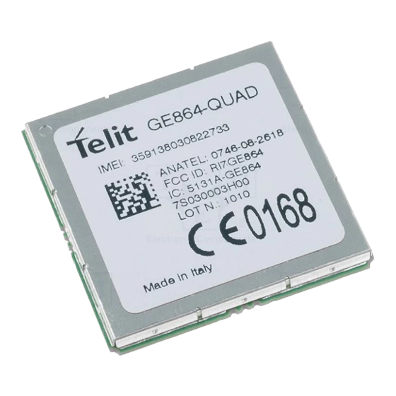
- Page 1 GE864 QUAD V2 Hardware User Guide 1vv0300841 Rev.5 – 2017-05-11...
-
Page 2: Applicability Table
GE864-QUAD V2 Hardware User Guide 1vv0300841 Rev.5 – 2017-05-11 APPLICABILITY TABLE PRODUCT GE864-QUAD V2 Reproduction forbidden without Telit Communications S.p.A. written authorization - All Rights Reserved. Page 2 of 77... - Page 3 GE864-QUAD V2 Hardware User Guide 1vv0300841 Rev.5 – 2017-05-11 DISCLAIMER The information contained in this document is the proprietary information of Telit Communications S.p.A. and its affiliates (“TELIT”). The contents are confidential and any disclosure to persons other than the officers, employees, agents or subcontractors of the owner or licensee of this document, without the prior written consent of Telit, is strictly prohibited.
-
Page 4: Table Of Contents
GE864-QUAD V2 Hardware User Guide 1vv0300841 Rev.5 – 2017-05-11 Contents APPLICABILITY TABLE .............................. 2 1. INTRODUCTION ..............6 1.1. S COPE .................................. 6 1.2. A UDIENCE ................................6 1.3. C ONTACT NFORMATION UPPORT ........................6 1.4. D OCUMENT RGANIZATION ............................ 7 1.5. - Page 5 GE864-QUAD V2 Hardware User Guide 1vv0300841 Rev.5 – 2017-05-11 10.2.2. Output Lines Characteristics ....................53 GENERAL PURPOSE I/O ............55 11.1. GPIO L OGIC EVELS ........................... 56 11.2. GPIO P INPUT ......................... 57 SING A AD AS 11.3. GPIO P OUTPUT .......................
-
Page 6: Introduction
GE864-QUAD V2 Hardware User Guide 1vv0300841 Rev.5 – 2017-05-11 Introduction 1.1. Scope The aim of this document is the description of some hardware solutions useful for developing a product with the Telit GE864-QUAD V2 module. 1.2. Audience This document is intended for Telit customers, who are integrators, about to implement their applications using our GE864-QUAD V2 module. -
Page 7: Document Organization
GE864-QUAD V2 Hardware User Guide 1vv0300841 Rev.5 – 2017-05-11 1.4. Document Organization This document contains the following chapters: Chapter 1: “Introduction” provides a scope for this document, target audience, contact and support information, and text conventions. Chapter 2: “Overview” provides an overview of the document. Chapter 3: “GE864-QUAD V2 Mechanical Dimensions”... -
Page 8: Text Conventions
GE864-QUAD V2 Hardware User Guide 1vv0300841 Rev.5 – 2017-05-11 1.5. Text Conventions Danger – This information MUST be followed or catastrophic equipment failure or bodily injury may occur. Caution or Warning – Alerts the user to important points about integrating the module, if these points are not followed, the module and end user equipment may fail or malfunction. -
Page 9: Document History
GE864-QUAD V2 Hardware User Guide 1vv0300841 Rev.5 – 2017-05-11 1.7. Document History ISSUE#0 2009-01-07 Release First ISSUE# 0 ISSUE#1 2009-07-27 Changed par. 4.1 Turning ON and par. 5.1 Power supply Requirements Changed par. 12.3 Recommended foot print…. and par.14 Conformity Assessment Issues ISSUE#2 2009-10-21... -
Page 10: Overview
GE864-QUAD V2 Hardware User Guide 1vv0300841 Rev.5 – 2017-05-11 Overview In this document all the basic functions of a mobile phone are taken into account; for each one of them a proper hardware solution is suggested and eventually the wrong solutions and common errors to be avoided are evidenced. -
Page 11: Ge864-Quad V2 Mechanical Dimensions
GE864-QUAD V2 Hardware User Guide 1vv0300841 Rev.5 – 2017-05-11 GE864-QUAD V2 Mechanical Dimensions The Telit GE864-QUAD V2 module overall dimensions are: Length: 30 mm Width: 30 mm Thickness: 2,9 mm Weight: 4.2g Reproduction forbidden without Telit Communications S.p.A. written authorization - All Rights Reserved. -
Page 12: Ge864-Quad V2 Module Connections
GE864-QUAD V2 Hardware User Guide 1vv0300841 Rev.5 – 2017-05-11 GE864-QUAD V2 Module Connections 4.1. PIN-OUT The GE864-QUAD V2 uses 11x11 array BGA technology connection Internal Ball Signal Function Type PULL UP Audio Handsfree switching 100K CMOS 2.8V Handsfree mic. input; phase +, nom. MIC_HF+ Audio level 3mVrms... - Page 13 GE864-QUAD V2 Hardware User Guide 1vv0300841 Rev.5 – 2017-05-11 Internal Ball Signal Function Type PULL UP C103/TXD Serial data input (TXD) from DTE CMOS 2.8V Output for Data set ready signal (DSR) C107/DSR CMOS 2.8V to DTE Input for Request to send signal (RTS) C105/RTS CMOS 2.8V from DTE...
- Page 14 GE864-QUAD V2 Hardware User Guide 1vv0300841 Rev.5 – 2017-05-11 Internal Ball Signal Function Type PULL UP Ground Power Ground Power Ground Power Ground Power Ground Power Ground Power Ground Power Ground Power Ground Power Ground Power Ground Power Ground Power RESERVED Reserved Reserved...
- Page 15 GE864-QUAD V2 Hardware User Guide 1vv0300841 Rev.5 – 2017-05-11 Internal Ball Signal Function Type PULL UP Reserved Reserved Reserved Reserved Reserved Reserved Reserved Reserved Reserved Reserved Reserved Reserved Reserved Reserved Reserved Reserved Reserved Reserved Reserved Reserved Reserved Reserved Reserved * Ref. to Digital Voice Interface Application Note 80000NT10004a.
- Page 16 GE864-QUAD V2 Hardware User Guide 1vv0300841 Rev.5 – 2017-05-11 Reproduction forbidden without Telit Communications S.p.A. written authorization - All Rights Reserved. Page 16 of 77...
- Page 17 GE864-QUAD V2 Hardware User Guide 1vv0300841 Rev.5 – 2017-05-11 NOTE: If not used, almost all pins must be left disconnected. The only exceptions are the following pins: Ball Signal Function J1, J2, K1, K2 VBATT Main power supply A1, A11, D6, F1, F11, H1, H2, J3, K3, K4, K5, K6, Ground L1, L2, L3, L6, L11...
-
Page 18: Bga Balls Layout
GE864-QUAD V2 Hardware User Guide 1vv0300841 Rev.5 – 2017-05-11 4.1.1. BGA Balls Layout TOP VIEW GPIO_01 VBATT VBATT RESET* GPIO_03 VRTC VBATT VBATT GPIO_04 GPIO_10 TX_DISAB / DVI_TX SIMVCC SERVICE Antenna GPIO_06 DVI_WA0 ON_OFF* / ALARM GPIO_02 C106 / C125/RING / JDR C108 / C103 /... - Page 19 GE864-QUAD V2 Hardware User Guide 1vv0300841 Rev.5 – 2017-05-11 AUDIO Signals balls SIM CARD interface balls AUX UART&SERVICE Signals balls Prog. / data + Hw Flow Control signals balls ADC signals balls MISCELLANEOUS functions signals balls TELIT GPIO balls POWER SUPPLY VBATT balls POWER SUPPLY GND balls...
-
Page 20: Hardware Commands
GE864-QUAD V2 Hardware User Guide 1vv0300841 Rev.5 – 2017-05-11 Hardware Commands 5.1. Turning ON the GE864-QUAD V2 To turn ON the GE864-QUAD V2 the pad ON# must be tied low for at least 1 second and then released. When the power supply voltage is lower than 3.4V the pad ON# must be tied low for at least 4 seconds. - Page 21 GE864-QUAD V2 Hardware User Guide 1vv0300841 Rev.5 – 2017-05-11 A flow chart showing the proper turn on procedure is displayed below: NOTE: In order to avoid a back powering effect it is recommended to avoid having any HIGH logic level signal applied to the digital pins of the module when is powered OFF or during an ON/OFF transition.
- Page 22 GE864-QUAD V2 Hardware User Guide 1vv0300841 Rev.5 – 2017-05-11 For example: 1- Let's assume you need to drive the ON# pad with a totem pole output from +1.8V up to 5V microcontroller Reproduction forbidden without Telit Communications S.p.A. written authorization - All Rights Reserved.
-
Page 23: Turning Off The Ge864-Quad V2
GE864-QUAD V2 Hardware User Guide 1vv0300841 Rev.5 – 2017-05-11 2- Let's assume you need to drive the ON# pad directly with an ON/OFF button: 5.2. Turning OFF the GE864-QUAD V2 The turning off of the device can be done in two ways: ... - Page 24 GE864-QUAD V2 Hardware User Guide 1vv0300841 Rev.5 – 2017-05-11 Either ways, when the device issues a detach request to the network informing that the device will not be reachable any more. To turn OFF the module the pad ON# must be tied low for at least 2 seconds and then released.
-
Page 25: Hardware Unconditional Restart
GE864-QUAD V2 Hardware User Guide 1vv0300841 Rev.5 – 2017-05-11 In order to avoid a back powering effect it is recommended to avoid having any HIGH logic level signal applied to the digital pins of the module when is powered OFF or during an ON/OFF transition. - Page 26 GE864-QUAD V2 Hardware User Guide 1vv0300841 Rev.5 – 2017-05-11 Do not use any pull up resistor on the RESET# line or any totem pole digital output. Using pull up resistor may bring to latch up problems on the module power regulator and improper functioning of the module.
-
Page 27: Power Supply
GE864-QUAD V2 Hardware User Guide 1vv0300841 Rev.5 – 2017-05-11 Power Supply The power supply circuitry and board layout are a very important part in the full product design and they strongly reflect on the product overall performances, hence read carefully the following requirements and guidelines for a proper design. -
Page 28: Power Consumption
GE864-QUAD V2 Hardware User Guide 1vv0300841 Rev.5 – 2017-05-11 6.2. Power Consumption The GE864-QUAD V2 power consumptions are: GE864-QUAD V2 Average Mode Mode description (mA) SWITCHED OFF Module supplied but Switched Off Switched Off <62 uA IDLE mode Normal mode: full functionality of the AT+CFUN=1 16.0 module... -
Page 29: General Design Rules
GE864-QUAD V2 Hardware User Guide 1vv0300841 Rev.5 – 2017-05-11 6.3. General Design Rules The principal guidelines for the Power Supply Design embrace three different design steps: the electrical design the thermal design the PCB layout. 6.3.1. Electrical Design Guidelines The electrical design of the power supply depends strongly from the power source where this power is drained. - Page 30 GE864-QUAD V2 Hardware User Guide 1vv0300841 Rev.5 – 2017-05-11 An example of linear regulator with 5V input is: 6.3.1.2. +12V input Source Power Supply Design Guidelines The desired output for the power supply is 3.8V, hence, due to the big difference between the input source and the desired output, a linear regulator is not suited and shall not be used.
- Page 31 GE864-QUAD V2 Hardware User Guide 1vv0300841 Rev.5 – 2017-05-11 Make sure the low ESR capacitor on the power supply output (usually a tantalum one) is rated at least 10V. As far as car applications, a spike protection diode must be inserted close to the power input, in order to clean the supply from spikes.
- Page 32 GE864-QUAD V2 Hardware User Guide 1vv0300841 Rev.5 – 2017-05-11 6.3.1.3. Battery Source Power Supply Design Guidelines The desired nominal output for the power supply is 3.8V and the maximum voltage allowed is 4.2V, hence a single 3.7V Li-Ion cell battery type is suited for supplying the power to the Telit GE864-QUAD V2 module.
-
Page 33: Thermal Design Guidelines
GE864-QUAD V2 Hardware User Guide 1vv0300841 Rev.5 – 2017-05-11 6.3.2. Thermal Design Guidelines The thermal design for the power supply heat sink must be done with the following specifications: Average current consumption during transmission @PWR level max: 500mA Average current consumption during transmission @ PWR level min: 100mA ... -
Page 34: Power Supply Pcb Layout Guidelines
GE864-QUAD V2 Hardware User Guide 1vv0300841 Rev.5 – 2017-05-11 This generated heat will be mostly conducted to the ground plane under the GE864-QUAD V2 ; you must ensure that your application can dissipate it. 6.3.3. Power Supply PCB Layout Guidelines As seen on the electrical design guidelines the power supply shall have a low ESR capacitor on the output to cut the current peaks and a protection diode on the input to protect... -
Page 35: Parameters For Atex Applications
GE864-QUAD V2 Hardware User Guide 1vv0300841 Rev.5 – 2017-05-11 This is done in order to reduce the radiated field (noise) at the switching frequency (100-500 kHz usually). The use of a good common ground plane is suggested. The placement of the power supply on the board must be done in such a way to guarantee that the high current return paths in the ground plane are not overlapped to any noise sensitive circuitry as the microphone amplifier/buffer or earphone... -
Page 36: Antenna
GE864-QUAD V2 Hardware User Guide 1vv0300841 Rev.5 – 2017-05-11 Antenna The antenna connection and board layout design are the most important part in the full product design and they strongly reflect on the product overall performances, hence read carefully and follow the requirements and the guidelines for a proper design. -
Page 37: Ntenna - Pcb Line Guidelines
GE864-QUAD V2 Hardware User Guide 1vv0300841 Rev.5 – 2017-05-11 This line of transmission shall fulfill the following requirements: ANTENNA LINE ON PCB REQUIREMENTS Impedance 50 ohm 0,3 dB Attenuation No coupling with other signals allowed Cold End (Ground Plane) of antenna shall be equipotential to the GE864-QUAD V2 ground pins Furthermore if the device is developed for the US market and/or Canada market, it shall comply to the FCC and/or IC... -
Page 38: Ntenna - Installation Guidelines
GE864-QUAD V2 Hardware User Guide 1vv0300841 Rev.5 – 2017-05-11 Keep the antenna line far away from the GE864-QUAD V2 power supply lines; If you have EM noisy devices around the PCB hosting the GE864-QUAD V2, such as fast switching ICs, take care of the shielding of the antenna line by burying it inside the layers of PCB and surround it with Ground planes, or shield it with a metal frame cover. -
Page 39: Logic Level Specifications
GE864-QUAD V2 Hardware User Guide 1vv0300841 Rev.5 – 2017-05-11 Logic Level Specifications Where not specifically stated, all the interface circuits work at 2.8V CMOS logic levels. The following table shows the logic level specifications used in the Telit GE864-QUAD V2 interface circuits: Absolute Maximum Ratings –... - Page 40 GE864-QUAD V2 Hardware User Guide 1vv0300841 Rev.5 – 2017-05-11 Level Typical Output Current Input Current Reproduction forbidden without Telit Communications S.p.A. written authorization - All Rights Reserved. Page 40 of 77...
-
Page 41: Reset Signal
GE864-QUAD V2 Hardware User Guide 1vv0300841 Rev.5 – 2017-05-11 8.1. Reset Signal Signal Function Ball Number RESET Reset RESET is used to reset the GE864-QUAD V2 modules. Whenever this signal is pulled low, the GE864-QUAD V2 is reset. When the device is reset it stops any operation. After the release of the reset GE864-QUAD V2 is unconditionally shut down, without doing any detach operation from the network where it is registered. - Page 42 GE864-QUAD V2 Hardware User Guide 1vv0300841 Rev.5 – 2017-05-11 to permit to the internal circuitry the power on reset and under voltage lockout functions. Reproduction forbidden without Telit Communications S.p.A. written authorization - All Rights Reserved. Page 42 of 77...
-
Page 43: Serial Ports
GE864-QUAD V2 Hardware User Guide 1vv0300841 Rev.5 – 2017-05-11 Serial Ports The serial port on the Telit GE864-QUAD V2 is the core of the interface between the module and OEM hardware. 2 serial ports are available on the module: MODEM SERIAL PORT (Main, ASC0) ... - Page 44 GE864-QUAD V2 Hardware User Guide 1vv0300841 Rev.5 – 2017-05-11 Output high 2.2V 3.0V level V Output low level 0.35V The table below shows the signals of the GE864-QUAD V2 serial port: RS232 Signal GE864-QUAD Name Usage V2 Pad Number Number DCD –...
-
Page 45: Evel Translation
GE864-QUAD V2 Hardware User Guide 1vv0300841 Rev.5 – 2017-05-11 In order to avoid a back powering effect it is recommended to avoid having any HIGH logic level signal applied to the digital pins of the module when is powered OFF or during an ON/OFF transition. - Page 46 GE864-QUAD V2 Hardware User Guide 1vv0300841 Rev.5 – 2017-05-11 This is because in this way the level translator IC outputs on the module side (i.e. GE864 inputs) will work at +3.8V interface levels, damaging the module inputs. NOTE: In order to be able to do in circuit reprogramming of the GE864 firmware, the serial port on the Telit GE864 shall be available translation...
- Page 47 GE864-QUAD V2 Hardware User Guide 1vv0300841 Rev.5 – 2017-05-11 The RS232 serial port lines are usually connected to a DB9 connector with the following layout: Reproduction forbidden without Telit Communications S.p.A. written authorization - All Rights Reserved. Page 47 of 77...
-
Page 48: Evel Translation
GE864-QUAD V2 Hardware User Guide 1vv0300841 Rev.5 – 2017-05-11 9.3. 5V UART Level Translation If the OEM application uses a microcontroller with a serial port (UART) that works at a voltage different from 2.8 – 3V, then a circuitry has to be provided to adapt the different levels of the two set of signals. - Page 49 GE864-QUAD V2 Hardware User Guide 1vv0300841 Rev.5 – 2017-05-11 NOTE: The UART input line TXD (rx_uart) of the GE864-QUAD V2 is NOT internally pulled up with a resistor, so there may be the need to place an external 47KΩ pull-up resistor, either the DTR (dtr_uart) and RTS (rts_uart) input lines are not pulled up internally, so an external pull-up resistor of 47KΩ...
-
Page 50: Audio Section Overview
GE864-QUAD V2 Hardware User Guide 1vv0300841 Rev.5 – 2017-05-11 Audio Section Overview The first Baseband chip was developed for the cellular phones, which needed two separated amplifiers both in RX and in TX section. A couple of amplifiers had to be used with internal audio transducers while the other couple of amplifiers had to be used with external audio transducers. - Page 51 GE864-QUAD V2 Hardware User Guide 1vv0300841 Rev.5 – 2017-05-11 Reproduction forbidden without Telit Communications S.p.A. written authorization - All Rights Reserved. Page 51 of 77...
-
Page 52: Electrical Characteristics
GE864-QUAD V2 Hardware User Guide 1vv0300841 Rev.5 – 2017-05-11 10.2. Electrical Characteristics TIP: Being the microphone circuitry the more noise sensitive, its design and layout must be done with particular care. Both microphone paths are balanced and the OEM circuitry must be balanced designed to reduce the common mode noise typically generated on the ground plane. -
Page 53: Output Lines Characteristics
GE864-QUAD V2 Hardware User Guide 1vv0300841 Rev.5 – 2017-05-11 10.2.2. Output Lines Characteristics TIP: We suggest driving the load differentially from both output drivers, thus the output swing will double and the need for the output coupling capacitor avoided. However if particular OEM application needs also a Single Ended circuitry can be implemented, but the output power will be reduced four times. - Page 54 GE864-QUAD V2 Hardware User Guide 1vv0300841 Rev.5 – 2017-05-11 “EAR_MT” Output Lines line coupling single-ended differential 0dBFS normalized gain 3,7 V differential output load ≥ 16 Ω -12dBFS resistance internal output 4Ω ( typical resistance signal bandwidth 150 - 4000 Hz 3 dB maximal full scale...
-
Page 55: General Purpose I/O
GE864-QUAD V2 Hardware User Guide 1vv0300841 Rev.5 – 2017-05-11 General Purpose I/O The general-purpose I/O pads can be configured to act in three different ways: Input Output Alternate function (internally controlled) Input pads can only be read and report the digital value (high or low) present on the pad at the read time;... -
Page 56: Gpio Logic Levels
GE864-QUAD V2 Hardware User Guide 1vv0300841 Rev.5 – 2017-05-11 Not all GPIO pads support all these three modes: GPIO2 supports all three modes and can be input, output, Jamming Detect Output (Alternate function) GPIO4 supports all three modes and can be input, output, RF Transmission Control (Alternate function) ... -
Page 57: Using Agpio Pad As Input
GE864-QUAD V2 Hardware User Guide 1vv0300841 Rev.5 – 2017-05-11 11.2. Using a GPIO Pad as INPUT The GPIO pads, when used as inputs, can be connected to a digital output of another device and report its status, provided this device has interface levels compatible with the 2.8V CMOS levels of the GPIO. -
Page 58: Using The Rftxmon Output Gpio5
GE864-QUAD V2 Hardware User Guide 1vv0300841 Rev.5 – 2017-05-11 11.5. Using the RFTXMON Output GPIO5 GPIO5 pin, when configured RFTXMON Output, controlled by the GE864-QUAD Automotive V2 module and will rise when transmitter active fall after transmitter activity is completed. There are 2 different modes for this function: 1) Active during all the calls: For example, if a call is started, the line will be HIGH... -
Page 59: Using The Buzzer Output Gpio7
GE864-QUAD V2 Hardware User Guide 1vv0300841 Rev.5 – 2017-05-11 11.7. Using the Buzzer Output GPIO7 The GPIO7 pad, when configured as Buzzer Output, is controlled by the GE864-QUAD Automotive V2 module and will drive with appropriate square waves a Buzzer driver. This permits to your application to easily implement Buzzer feature with... -
Page 60: Using The Temperature Monitor Function
GE864-QUAD V2 Hardware User Guide 1vv0300841 Rev.5 – 2017-05-11 11.8. Using the Temperature Monitor Function 11.8.1. Short Description The Temperature Monitor is a function of the module that permits to control its internal temperature and if properly set (see the #TEMPMON command on AT Interface guide) it raise to High Logic level a GPIO when the maximum temperature is reached. -
Page 61: Indication Of Network Service Availability
GE864-QUAD V2 Hardware User Guide 1vv0300841 Rev.5 – 2017-05-11 If the set command is enable the alternate function is not usable. 11.9. Indication of Network Service Availability The STAT_LED pin status shows information on the network service availability and Call status. In the GE864-QUAD V2 modules, the STAT_LED usually needs an external transistor to drive an external LED. -
Page 62: Ypass Out
GE864-QUAD V2 Hardware User Guide 1vv0300841 Rev.5 – 2017-05-11 11.10. RTC Bypass Out The VRTC pin brings out the Real Time Clock supply, which is separate from the rest of the digital part, allowing having only RTC going on when all the other parts of the device are off. -
Page 63: Dac And Adc Converter
GE864-QUAD V2 Hardware User Guide 1vv0300841 Rev.5 – 2017-05-11 DAC and ADC Converter 12.1. DAC Converter 12.1.1. Description Internal Ball Signal I/O Function Type Pull up DAC Converter DAC_OUT Digital/Analog converter output The GE864-QUAD V2 module provides one Digital to Analog Converter. -
Page 64: Enabling Dac
GE864-QUAD V2 Hardware User Guide 1vv0300841 Rev.5 – 2017-05-11 12.1.2. Enabling DAC The AT command below is available to use the DAC function: AT#DAC[=<enable>[,<value>]] <value> – scale factor of the integrated output voltage (0– 1023, with 10 bit precision), and it must be present if <enable>=1. -
Page 65: Adc Converter
GE864-QUAD V2 Hardware User Guide 1vv0300841 Rev.5 – 2017-05-11 12.2. ADC Converter 12.2.1. Description Internal Ball Signal I/O Function Type Pull up ADC Converters ADC_IN1 Analog/Digital converter input ADC_IN2 Analog/Digital converter input The GE864-QUAD V2 module provides three Analog to Digital Converter. -
Page 66: Debug Of The Ge864-Quad V2 In Production
GE864-QUAD V2 Hardware User Guide 1vv0300841 Rev.5 – 2017-05-11 12.3. Debug of the GE864-QUAD V2 in Production To test and debug the mounting of the GE864-QUAD V2, we strongly recommend to foreseen test pads on the host PCB, in order to check the connection between the GE864-QUAD V2 itself and the application and to test the performance of the module connecting it with an external computer. -
Page 67: Assembly The Ge864-Quad V2 On The Board
GE864-QUAD V2 Hardware User Guide 1vv0300841 Rev.5 – 2017-05-11 Assembly the GE864-QUAD V2 on the Board The Telit GE864-QUAD V2 have been designed in order to be compliant with the standard lead-free SMT process. Pin A1 Lead-free Alloy: Surface finishing Sn/Ag/Cu for all solder pads Reproduction forbidden without Telit Communications S.p.A. -
Page 68: Recommended Foot Print For The Application
GE864-QUAD V2 Hardware User Guide 1vv0300841 Rev.5 – 2017-05-11 13.1. Recommended foot print for the application In order to easily rework the GE864-QUAD V2 module is suggested to consider on the application a 1.5mm inhibit area around the module. It is also suggested, as common rule for a SMT component, to avoid having a mechanical part of the application in direct contact with the module. -
Page 69: Stencil
GE864-QUAD V2 Hardware User Guide 1vv0300841 Rev.5 – 2017-05-11 13.2. Stencil Stencil apertures layout can be the same of the recommended footprint (1:1), we suggest a thickness of stencil foil >120µm. 13.3. PCB pad design Non solder mask defined” (NSMD) type is recommended for the solder pads on the PCB. -
Page 70: Solder Paste
GE864-QUAD V2 Hardware User Guide 1vv0300841 Rev.5 – 2017-05-11 Holes in pad are allowed only for blind holes and not for through holes. Recommendations for PCB pad surfaces: Finish Layer thickness Properties [µm] good solder ability Electro-less 3 –7 / protection, Ni / 0.05 –... -
Page 71: Ge865 Solder Reflow
GE864-QUAD V2 Hardware User Guide 1vv0300841 Rev.5 – 2017-05-11 13.4.1. GE865 Solder reflow The following is the recommended solder reflow profile Profile Feature Pb-Free Assembly Average ramp-up rate (T 3°C/second max to T Preheat – Temperature Min (Tsmin) 150°C – Temperature Max (Tsmax) 200°C –... - Page 72 GE864-QUAD V2 Hardware User Guide 1vv0300841 Rev.5 – 2017-05-11 NOTE: All temperatures refer to topside of the package, measured on the package body surface WARNING: The GE865 module withstands one reflow process only. Reproduction forbidden without Telit Communications S.p.A. written authorization - All Rights Reserved.
-
Page 73: Packing System
GE864-QUAD V2 Hardware User Guide 1vv0300841 Rev.5 – 2017-05-11 Packing system The GE864-QUAD V2 are packaged on trays of 20 pieces each. This is especially suitable for the GE864-QUAD V2 according to SMT processes for pick & place movement requirements. Section A- The size of the tray is: 329 x 176mm. -
Page 74: Moisture Sensibility
GE864-QUAD V2 Hardware User Guide 1vv0300841 Rev.5 – 2017-05-11 WARNING: These trays can withstand at the maximum temperature of 65° C. NOTE: All temperatures refer to topside of the package, measured on the package body surface 14.1. Moisture sensibility The level of moisture sensibility of GE864-QUAD V2 is “3”, in according with standard IPC/JEDEC J-STD-020, take care all the relatives requirements for using this kind of components. -
Page 75: Ge864 Orientation On The Tray
GE864-QUAD V2 Hardware User Guide 1vv0300841 Rev.5 – 2017-05-11 14.2. GE864 orientation on the tray Reproduction forbidden without Telit Communications S.p.A. written authorization - All Rights Reserved. Page 75 of 77... -
Page 76: Safety Recommendations
GE864-QUAD V2 Hardware User Guide 1vv0300841 Rev.5 – 2017-05-11 SAFETY RECOMMENDATIONS NOTE: Read this section carefully to ensure the safe operation. Be sure the use of this product is allowed in the country and in the environment required. The use of this product may be dangerous and has to be avoided in the following areas: ... - Page 77 GE864-QUAD V2 Hardware User Guide 1vv0300841 Rev.5 – 2017-05-11 The European Community provides some Directives for the radio equipment introduced on the market. All the relevant information’s are available on the European Community website: https://ec.europa.eu/growth/single-market/european-standards/harmonised-standards/rtte_en The text of the Directive 2014/53/EU regarding radio equipment is available at: http://eur-lex.europa.eu/legal-content/EN/TXT/?qid=1429097565265&uri=CELEX:32014L0053 Reproduction forbidden without Telit Communications S.p.A.
Need help?
Do you have a question about the GE864 QUAD V2 and is the answer not in the manual?
Questions and answers