
Related Manuals for Telit Wireless Solutions LE920


Summary of Contents for Telit Wireless Solutions LE920
-
Page 2: Applicability Table
APPLICABILITY TABLE 1... - Page 3 SPECIFICATIONS SUBJECT TO CHANGE WITHOUT NOTICE Notice While reasonable efforts have been made to assure the accuracy of this document, Telit assumes no liability resulting from any inaccuracies or omissions in this document, or from use of the information obtained herein. The information in this document has been carefully checked and is believed to be entirely reliable.
- Page 4 Usage and Disclosure Restrictions License Agreements The software described in this document is the property of Telit and its licensors. It is furnished by express license agreement only and may be used only in accordance with the terms of such an agreement. Copyrighted Materials Software and documentation are copyrighted materials.
- Page 5 Contents...
- Page 9 The aim of this document is to present possible and recommended hardware solutions useful for developing a product with the Telit LE920 module. All the features and solutions detailed are applicable to all LE920, where “LE920” refers to the modules listed in the applicability table.
- Page 10 Chapter 2: “General Product Description” gives an overview of the features of the product. Chapter 3: “LE920 Module Connections” deals with the pin out configuration and layout. Chapter 4: “Hardware Commands” instructs how to control the module via hardware Chapter 5: “Power Supply”...
- Page 11 Tip or Information – Provides advice and suggestions that may be useful when integrating the module. All dates are in ISO 8601 format, i.e. YYYY-MM-DD. LE920-EUG/NAG Product Description, 80407ST10118A LE920-EUG/NAG AT command reference guide, 80407ST10116A Telit EVK2 User Guide, 1vv0300704 Telit xE920 Audio Settings Application Note, 80404NT10095A...
- Page 12 Whereas the suggested hardware configurations need not be considered mandatory, the information given should be used as a guide and a starting point for properly developing your product with the Telit LE920 module. NOTICE: The integration of the GSM/GPRS/EGPRS/WCDMA/HSPA+/LTE LE920 cellular module within user application must be done according to the design rules described in this manual.
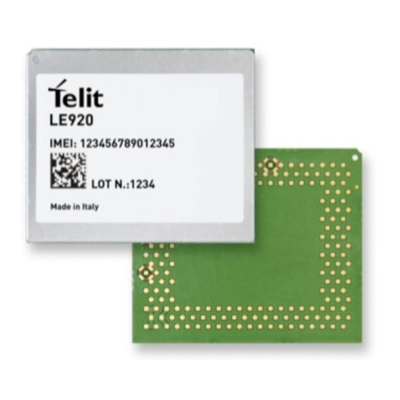
- Page 13 The Telit LE920 module overall dimensions are: • Length: 34 mm , +/- 0.15 mm Tolerance • Width: 40 mm , +/- 0.15 mm Tolerance • Thickness: 2.9 mm , +/- 0.13 mm Tolerance The module weight of LE920 is about 9.0 gram.
- Page 14 ETSI specifications. –40°C ~ +85°C Storage and non-operating Temperature Range As a part of Telit corporate policy of environmental protection, the LE920 complies with the RoHS (Restriction of Hazardous Substances) directive of the European Union (EU directive 2011/65/EU).
- Page 15 80MHz Tx: 9612 ~ 9888 WCDMA2100 – B1 1920 ~ 1980 2110 ~ 2170 190MHz Rx: 10562 ~ 10838 (LE920 NA/EU/NV) Tx: 9262 ~ 9538 WCDMA1900 – B2 1850 ~ 1910 1930 ~ 1990 80MHz Rx: 9662 ~ 9938 (LE920-NA/NV only) WCDMA1800 –...
- Page 16 Tx: 24150 ~ 24449 832 ~ 862 791 ~ 821 -41MHz (LE920-EU only) Rx: 6150 ~ 6449 LE920 maximum sensitivity levels are as follow: -113 dBm @ 2G -112 dBm @ 3G -102 dBm @ 4G (BW=5MHz)
- Page 17 Signal Function Type COMMENT USB HS 2.0 Communication Port USB_D+ I/O USB differential Data(+) USB_D- I/O USB differential Data(+) USB_VBUS AI Power sense for the internal USB transceiver Power Asynchronous UART – Prog. / data +HW Flow Control AH19 C103/TXD Serial data input (TXD) from DTE 1.8V AF19 C104/RXD...
- Page 18 Signal Function Type COMMENT I/O GPIO_03 1.8V GPIO_03 I/O GPIO_04 1.8V GPIO_04 I/O GPIO_05 1.8V GPIO_05 I/O GPIO_06 1.8V GPIO_06 I/O GPIO_07 1.8V GPIO_07 I/O GPIO_08 1.8V GPIO_08 I/O GPIO_09 1.8V GPIO_09 I/O GPIO_10 1.8V GPIO_10 RF Section Antenna I/O GSM/EDGE/UMTS/LTE Antenna (50 Ohm) ANT_DIV UMTS/LTE Antenna Diversity Input (50 Ohm) GPS Section...
- Page 19 Signal Function Type COMMENT Ground Ground Ground Ground Ground Ground Ground Ground Ground Ground Ground Ground Ground Ground Ground Ground Ground Ground Ground Ground Ground Ground Ground Ground Ground Ground Ground Ground Ground Ground Ground AK17 GND Ground AL18 GND Ground AM17 GND Ground...
- Page 20 Signal Function Type COMMENT AP11 GND Ground AP13 GND Ground AP15 GND Ground Ground Ground Ground Ground AR10 GND Ground AR12 GND Ground AR14 GND Ground AR16 GND Ground Ground Ground Ground AS11 GND Ground AS13 GND Ground AS15 GND Ground Ground Ground...
- Page 21 Signal Function Type COMMENT Reserved Reserved Reserved Reserved Reserved Reserved Reserved Reserved Reserved Reserved Reserved Reserved Reserved Reserved Reserved Reserved Reserved Reserved Reserved Reserved Reserved Reserved Reserved Reserved Reserved Reserved Reserved Reserved Reserved Reserved Reserved Reserved Reserved Reserved Reserved Reserved Reserved Reserved Reserved...
- Page 22 When the UART signals are used as the communication port between the Host and the Modem: DTR pin must be connected in order to enter LE920’s power saving mode. RI pin must be connected in order to wake the host when a call is coming during sleep mode of host.
- Page 23 AT6,AT8,AT10,AT12,AT14,AT16,AU1,AU5,AU7, AU11,AU15 ON/OFF*...
- Page 24 NOTE: The pin defined as must be considered RESERVED and not connected to any pin in the application. The related area on the application must be kept empty.
- Page 25 To turn on LE920, the pad ON# must be tied low for at least 1 second and then released. The maximum current that can be drained from the ON# pad is 0.1 mA. A simple circuit to power on the module is illustrated below: Upon turning on LE920 module, The LE920 is not activated yet because the boot sequence of LE920 is still going on internally.
- Page 26 NOTE: To check if the LE920 has powered on, the hardware line PWRMON must be monitored. When PWRMON goes high, the module has powered on. NOTE: Do not use any pull up resistor on the ON# line, it is internally pulled up. Using pull up resistor may cause latch-up problems on the LE920 power regulator and improper powering on/off of the module.
- Page 27 Turning off the device can be done in three ways: by Software command by Hardware shutdown by Hardware Unconditional Restart by Hardware Unconditional shutdown When the device is shut down by software command or by hardware shutdown, it issues to the network a detach request that informs the network that the device will not be reachable any more.
- Page 28 LE920 can be shut down by a software command. When a shut down command is sent, LE920 goes into the finalization state and finally will shut down PWRMON at the end of this state. The duration of the finalization state can differ according to the situation in which the LE920 is, so a value cannot be defined.
- Page 29 To turn OFF LE920 the pad ON/OFF# must be tied low for at least 2 seconds and then released. The same circuitry and timing for the power on must be used. When the hold time of ON/OFF# is above 2 seconds, LE920 goes into the finalization state and finally will shut down PWRMON at the end of this state.
- Page 30 To unconditionally restart LE920, the pad RESET# must be tied low for period between 500 - 2000 milliseconds and then released. A simple circuit to do it is: RESET# 500mSec < < 2000mSec RESET Unconditional Restart impulse NOTE: Do not use any pull up resistor on the RESET# line or any totem pole digital output. Using pull up resistor may cause latch-up problems on the LE920 power regulator and improper functioning of the module.
- Page 31 Let us assume you need to drive the RESET# pad with a totem pole output of a +1.8/5 V microcontroller (uP_OUT2): +1.8 / 5V To unconditionally Shutdown LE920, the pad SHDN_N must be tied low for at least 200 milliseconds and then released. A simple circuit to do it is:...
- Page 32 Do not use any pull up resistor on the SHDN_N line or any totem pole digital output. Using pull up resistor may cause latch-up problems on the LE920 power regulator and improper functioning of the module. The line SHDN_N must be connected only in open collector configuration.
- Page 33 The power supply circuitry and board layout are a very important part in the full product design and they strongly reflect on the overall product performance. Reading carefully the requirements and the guidelines that follow will ensure a good and proper design. The LE920 power requirements are: Power Supply Nominal Supply Voltage 3.8V...
- Page 34 GSM900 PL5 GPRS Sending data mode DCS1800 PL0 EDGE 4TX + 1RX GSM900 PL5 EDGE Sending data mode DCS1800 PL0 * Worst/best case depends on network configuration and is not under module control. TIP: The electrical design for the Power supply must be made ensuring that it will be capable of a peak current output of at least 2A.
- Page 35 A Bypass low ESR capacitor of adequate capacity must be provided in order to cut the current absorption peaks close to LE920, a 100μF tantalum capacitor is usually suitable. Make sure the low ESR capacitor on the power supply output (usually a tantalum one) is rated at least 10V.
- Page 36 A protection diode must be inserted close to the power input, in order to protect LE920 from power polarity inversion. This can be the same diode as for spike protection. An example of switching regulator with 12V input is in the below schematic (it is split in 2...
- Page 37 Switching regulator...
- Page 38 LE920 and damage it. NOTE: Do not use any Ni-Cd, Ni-MH, and Pb battery types directly connected with LE920. Their use can lead to overvoltage on LE920 and damage it. Use only Li-Ion battery types. ...
- Page 39 For the heat generated by the LE920, you can consider it to be during transmission 2W max during class12 GPRS upload. This generated heat will be mostly conducted to the ground plane under the LE920;...
- Page 40 If your application does not have audio interface but only uses the data feature of the Telit LE920, then this noise is not so disturbing and power supply layout design can be more forgiving.
- Page 41 The power supply input cables must be kept separate from noise sensitive lines such as microphone/earphone cables.
- Page 42 LE920 antenna pad (AD1) by means of a transmission line implemented on the PCB. In the case that the antenna is not directly connected to the antenna pad of the LE920, then a PCB line is required in order to connect with it or with its connector.
- Page 43 End-Users must be provided with transmitter operation conditions for satisfying RF exposure compliance. OEM integrators must ensure that the end user has no manual instructions to remove or install the LE920 module. Antennas used for this OEM module must not exceed 3dBi gain for mobile and fixed operating configurations.
-
Page 44: Antenna Requirements
50Ω Impedance VSWR recommended ≤ 2:1 When using the Telit LE920, since there’s no antenna connector on the module, the antenna must be connected to the LE920 antenna pad (AU9) by means of a transmission line implemented on the PCB. - Page 45 In the case that the antenna is not directly connected at the antenna pad of the LE920, then a PCB line is required in order to connect with it or with its connector. The second Rx antenna should not be located in the close vicinity of the main antenna. In...
- Page 46 When using the Telit LE920, since there’s no antenna connector on the module, the antenna must be connected to the LE920 through the PCB to the antenna pad. In the case that the antenna is not directly connected at the antenna pad of the LE920, then a PCB line is required.
- Page 47 Ground planes; or shield it with a metal frame cover. If you do not have EM-noisy devices around the PCB of LE920, use a Micro strip line on the surface copper layer for the antenna line. The line attenuation will be lower than a buried one.
- Page 48 The following table shows the logic level specifications used in the Telit LE920 interface circuits: NOTE: Do not connect LE920’s digital logic signal directly to OEM’s digital logic signal with a level higher than 2.7V for 1.8V CMOS signals. For 1.8V CMOS signals:...
- Page 49 USB and not possible via UART. The reason is that Telit consider it impractical to transfer firmware binaries exceeding 100Mb via UART. The USB port on the Telit LE920 is typically the main interface between the module and OEM hardware.
- Page 50 The only configuration that does not need a level translation is the 1.8V UART. The serial port 1 on LE920 is a +1.8V UART with all the 7 RS232 signals. It differs from the PC-RS232 in signal polarity (RS232 is reversed) and levels.
- Page 51 According to V.24, RX/TX signal names are referred to the application side, therefore on the LE920 side these signal are in the opposite direction: TXD on the application side will be connected to the receive line (here named TXD/ rx_uart ) of the LE920 serial port and vice versa for RX.
- Page 52 Serial port 2 on the LE920 is a +1.8V UART with only the RX and TX signals. The signals of the LE920 serial port are: Signal Function Type COMMENT TXD_AUX O Auxiliary UART (TX Data to DTE) 1.8V AB19 RXD_AUX I Auxiliary UART (RX Data to DTE) 1.8V...
- Page 53 An example of RS232 level adaption circuitry could be accomplished using a MAXIM transceiver (MAX218). In this case the chipset is capable of translating directly from 1.8V to the RS232 levels (Example on 4 signals only). NOTE: In this case the length of the lines on the application must be taken into account to avoid problems in the case of High-speed rates on RS232.
- Page 54 WARNING: LE920 Analog audio implementation uses an internal CODEC. LE920 internal codec uses the same external LE920 digital Audio interface signals Therefore, applications that are using analog audio, must make sure that the digital audio interface shall be either not connected, or Hi-Z, or ‘input’ to Host application.
- Page 56 Input pads can only be read and report the digital value (high or low) present on the pad at the read time; output pads can only be written or queried and set the value of the pad output; an alternate function pad is internally controlled by the LE920 firmware and acts depending on the function implemented.
- Page 57 Where not specifically stated, all the interface circuits work at 1.8V CMOS logic levels. The following table shows the logic level specifications used in the LE920 interface circuits: For 1,8V signals: Absolute Maximum Ratings -Not Functional LE920 Parameter Input level on any -0.3V...
- Page 58 The GPIO pads, when used as outputs, can drive 1.8V CMOS digital devices or compatible hardware. When set as outputs, the pads have a push-pull output and therefore the pull-up resistor may be omitted. The Temperature Monitor is a function of the module that permits to control its internal temperature and if properly set (see the #TEMPMON command on AT Interface guide) it raises to High Logic level a GPIO when the maximum temperature is reached.
- Page 59 The STAT_LED pin status shows information on the network service availability and call status. In the LE920 modules, the STAT_LED usually needs an external transistor to drive an external LED. Because of the above, the status indicated in the following table is reversed...
- Page 60 The VRTC pin brings out the Real Time Clock supply, which is separate from the rest of the digital part, allowing having only the RTC operating when all the other parts of the device are off. To this power output a backup capacitor can be added in order to increase the RTC autonomy during power off of the battery.
- Page 61 Resolution < 6.6 The LE920 module provides 3 Analog to Digital Converters. An AT command is available to use the ADC function. The command is AT#ADC=1,2. The read value is expressed in mV Refer to SW User Guide or AT Commands Reference Guide for the full description of this...
- Page 62 The LE920 modules have been designed to be compliant with a standard lead-free SMT process.
- Page 63 In order to easily rework the LE920 it is suggested to consider that the application has a 1.5 mm placement inhibit area around the module. It is also suggested, as a common rule for an SMT component, to avoid having a mechanical part of the application in direct contact with the module.
- Page 64 Stencil’s apertures layout can be the same as the recommended footprint (1:1). A suggested thickness of stencil foil is greater than 120 µm. Non solder mask defined (NSMD) type is recommended for the solder pads on the PCB.
- Page 65 It is not recommended to place via or micro-via not covered by solder resist in an area of 0,3 mm around the pads unless it carries the same signal of the pad itself (see following figure). Holes in pad are allowed only for blind holes and not for through holes. Recommendations for PCB Pad Surfaces: Finish Layer thickness (um)
- Page 66 Solder Paste Lead free Sn/Ag/Cu We recommend using only “no clean” solder paste in order to avoid the cleaning of the modules after assembly. Recommended solder reflow profile:...
- Page 67 10-30 seconds Temperature (tp) Ramp-down Rate 6°C/second max. Time 25°C to Peak Temperature 8 minutes max. NOTE: All temperatures refer to topside of the package, measured on the package body surface. WARNING: The LE920 module withstands one reflow process only.
- Page 68 To test and debug the mounting of LE920, we strongly recommend foreseeing test pads on the host PCB, in order to check the connection between the LE920 itself and the application and to test the performance of the module by connecting it with an external computer.
- Page 69 When a sudden voltage is asserted to or cut from the power supplies, the steep transition makes some reactions such as overshoot and undershoot. This abrupt voltage transition can affect the device causing it to not work or make it malfunction.
- Page 70 LE920-EU/NA/NV contains an internal pull-up resistor on SIMIO. However, the un-mounted option in the application design can be recommended in order to tune R1 if necessary. The following Table lists the values of C1 to be adopted with the LE920 product: Product P/N C1 range (nF)
- Page 71 All LE920 signals are provided with some EMC protection. Nevertheless the accepted level differs according to which pin. The characteristics are described in the following Table: Signal Function Contact Power Supply AP17,AP19, AR18,AS17, VBATT_PA Main power supply ± 8KV ± 15KV...
- Page 72 One of the following options should be chosen in the design of host system in order to download or upgrade the Telit software and debug LE920 when LE920 is already mounted on a host system. Users who use both UART and USB interfaces to communicate with LE920...
- Page 73 The Telit LE920 is packaged on trays. Each tray contains 20 pieces as shown in the following picture:...
- Page 75 WARNING: These trays can withstand a maximum temperature of 65℃.
- Page 76 The LE920 is a Moisture Sensitive Device level 3, in accordance with standard IPC/JEDEC J- STD-020. Observe all of the requirements for using this kind of components. Calculated shelf life in sealed bag: 4 months at <40°C and <90% relative humidity (RH).
-
Page 77: Read Carefully
READ CAREFULLY Be sure that the use of this product is allowed in your country and in the environment required. The use of this product may be dangerous and must be avoided in the following areas: Where it can interfere with other electronic devices in environments such as hospitals, airports, aircrafts, etc. - Page 78 - Section 8, remove USB Low speed support - Section 10, adding Analog Audio support. - Section 14.4, update table Initial ‘official’ Release 2014-02-04 - Added LE920-NV support - Added VRTC support - Added Section 2.6, sensitivity - Section 8, added note - Section 13.3, update figure - Section 14.3, update description...
Need help?
Do you have a question about the LE920 and is the answer not in the manual?
Questions and answers