
Related Manuals for Telit Wireless Solutions LE910C1-NAD


Summary of Contents for Telit Wireless Solutions LE910C1-NAD
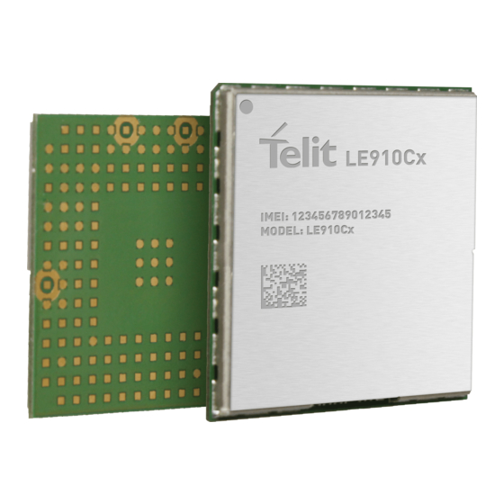
- Page 1 LE910Cx Hardware Design Guide 1VV0301298 Rev. 40 – 2023-03-16 Telit Technical Documentation...
-
Page 2: Applicability Table
APPLICABILITY TABLE This documentation applies to the following products: PRODUCTS DESCRIPTION LE910C1-NA North America – AT&T with global roaming LE910C1-NAD North America – AT&T with global roaming and Data only LE910C1-NS North America - Sprint variant LE910C1-AP APAC variant CAT1 variant... - Page 3 LE910Cx Hardware Design Guide Note: ‘X’ means ThreadX OS in LE910C1-EUX, LE910C1-SAX(D), LE910C1-SVX , LE910Cx-WWX(D) and LE910C1-APX. The other models which don’t have the letter ‘X’ are Linux OS. Note: Data only variants share the same HW of related voice variants and the voice features are disabled by SW.
-
Page 4: Table Of Contents
LE910Cx Hardware Design Guide CONTENTS APPLICABILITY TABLE CONTENTS INTRODUCTION Scope Audience Contact Information, Support Symbol Conventions Related Documents GENERAL PRODUCT DESCRIPTION Overview Applications General Functionality and Main Features Block Diagram Environmental Requirements 2.5.1. Temperature Range 2.5.2. RoHS Compliance Operating Frequency Bands 2.6.1. - Page 5 LE910Cx Hardware Design Guide Absolute Maximum Ratings – Not Operational Recommended Operating Conditions Logic Level Specifications 4.3.1. 1.8V Pads - Absolute Maximum Ratings 4.3.2. 1.8V Standard GPIOs 4.3.3. 1.8V SD Card Pads 4.3.4. 1.8V SIM Card Pads 4.3.5. Dual Voltage Pads - Absolute Maximum Ratings 4.3.6.
- Page 6 LE910Cx Hardware Design Guide GSM/WCDMA/TD-SCDMA/LTE Antenna – PCB Line Guidelines 64 GSM/WCDMA/LTE Antenna – Installation Guidelines Antenna Diversity Requirements GNSS Antenna Requirements 7.5.1. Combined GNSS Antenna 7.5.2. Linear and Patch GNSS Antenna 7.5.3. Front End Design Considerations 7.5.4. GNSS Antenna – PCB Line Guidelines 7.5.5.
- Page 7 LE910Cx Hardware Design Guide Indication of Software Ready RTC – Real Time Clock VAUX Power Output ADC Converter 9.5.1. Description 9.5.2. Using the ADC Converter Using the Temperature Monitor Function GNSS Characteristics MOUNTING THE MODULE ON YOUR BOARD General Finishing & Dimensions Recommended Footprint for the Application Stencil PCB Pad Design...
- Page 8 LE910Cx Hardware Design Guide APAC Approvals 13.2.1. Australia RCM 13.2.2. Japan JRL/JTBL Regulatory Notices 13.2.3. Taiwan NCC Regulatory Notices EMEA Approvals 13.3.1. EU RED Declaration of Conformity 13.3.1.1. RED Antennas 13.3.2. UK UKCA Declaration of Conformity Americas Approvals 13.4.1. USA FCC Approval 13.4.1.1.
- Page 9 LE910Cx Hardware Design Guide 14.2.6. Waiver of Liability Safety Recommendations GLOSSARY DOCUMENT HISTORY 1VV0301298 Rev.37 Page 9 of 149 2023-03-16 Not Subject to NDA...
-
Page 10: Introduction
LE910Cx Hardware Design Guide 1. INTRODUCTION Scope This document introduces the Telit LE910Cx module and presents possible and recommended hardware solutions for the development of a product based on this module. All the features and solutions described in this document are applicable to all LE910Cx variants listed in the applicability table. -
Page 11: Symbol Conventions
LE910Cx Hardware Design Guide Alternatively, use: https://www.telit.com/support For detailed information about where you can buy the Telit modules or for recommendations on accessories and components visit: https://www.telit.com To register for product news and announcements or for product questions contact Telit’s Technical Support Center (TTSC). - Page 12 LE910Cx Hardware Design Guide LE910Cx Interface Board HW User Guide 1VV0301323 LE910/LE920 Digital Voice Interface Application Note 80000NT11246A Telit_LE920A4_LE910Cx_Wi-Fi_Interface_Application_Note_r1 80490NT11511A Antenna Detection Application Note 80000NT10002A High-Speed Inter-Chip USB Electrical Specification, version 1.0 (a supplement to the USB 2.0 specification, Section 3.8.2) ETH_Expansion_board_Application Note 80490NT11622A ...
-
Page 13: General Product Description
LE910Cx Hardware Design Guide 2. GENERAL PRODUCT DESCRIPTION Overview LE910Cx is Telit’s new LTE series for IoT applications. In its most basic use case, the LE910Cx can be applied as a wireless communication front-end for telematics products, offering GNSS and mobile communication features to an external host CPU through its rich interfaces. -
Page 14: Applications
LE910Cx Hardware Design Guide The information presented in this document is believed to be accurate and reliable. However, no responsibility is assumed by Telit Communications S.p.A. for its use, nor any infringement of patents or other rights of third parties which may result from its use. No license is granted implicitly or in any other way under any patent rights of Telit Communications S.p.A. - Page 15 LE910Cx Hardware Design Guide Function Features Application processor Application processor to run customer application code 32-bit ARM Cortex-A7 up to 1.3 GHz running the Linux operating system Flash + DDR are large enough to allow for customer’s own software applications Interfaces Rich set of interfaces, including: SD/MMC Card Interface supporting SD3.0 standard...
-
Page 16: Block Diagram
LE910Cx Hardware Design Guide Note: The following interfaces are unique to the LE910Cx and may not be supported on other (former or future) xE910 family. Special care must be paid when designing the application board if future compatibility is required: - SGMII for Ethernet connectivity - SDIO for WIFI connectivity - SD/MMC for SD Card connectivity... - Page 17 LE910Cx Hardware Design Guide Application processor, Modem subsystem and Location processing with their external interfaces. These three functions are contained in a single SOC. RF front end and antenna ports. Digital Audio interface for external codec. Rich IO interfaces. Depending on the LE910Cx software features enabled, some of ...
-
Page 18: Environmental Requirements
LE910Cx Hardware Design Guide Environmental Requirements 2.5.1. Temperature Range Mode Temperature Note Operating temperature range -40 ~ +85°C Ambient. Ambient Temperatures outside of the range –20°C ÷ +55°C might slightly deviate from ETSI specifications. The module is fully functional, able to make and receive voice calls, data calls, SMS and GPRS traffic. - Page 19 HSPA+ LTE FDD SCDMA LE910C1-NA 2, 3, 5, 8 1, 2, 4, 5, 8 2, 4, 12 LE910C1-NAD 2, 3, 5, 8 1, 2, 4, 5, 8 2, 4, 12 LE910C1-NS 2, 4, 5, 12, 25, 26 LE910C1-AP 1, 5, 6, 8, 19...
-
Page 20: Reference Table Of Rf Bands Characteristics
LE910Cx Hardware Design Guide 2.6.2. Reference Table of RF Bands Characteristics Mode Freq. Tx (MHz) Freq. Rx (MHz) Channels Tx-Rx Offset PCS 1900 1850.2 ~ 1909.8 1930.2 ~ 1989.8 512 ~ 810 80 MHz DCS 1800 1710 ~ 1785 1805 ~ 1880 512 ~ 885 95 MHz GSM 850... - Page 21 LE910Cx Hardware Design Guide Mode Freq. Tx (MHz) Freq. Rx (MHz) Channels Tx-Rx Offset Tx: 19950 ~ 20399 LTE AWS – B4 1710 ~ 1755 2110 ~ 2155 400 MHz Rx: 1950 ~ 2399 Tx: 20400 ~ 20649 LTE 850 – B5 824 ~ 849 869 ~ 894 45 MHz...
- Page 22 LE910Cx Hardware Design Guide Mode Freq. Tx (MHz) Freq. Rx (MHz) Channels Tx-Rx Offset Tx: 37750 ~ 38250 LTE TDD 2600 – B38 2570 ~ 2620 2570 ~ 2620 0 MHz Rx: 37750 ~ 38250 Tx: 38250 ~ 38650 LTE TDD 1900 – B39 1880 ~ 1920 1880 ~ 1920 0 MHz...
-
Page 23: Rf Parameters
LE910Cx Hardware Design Guide RF Parameters 2.7.1. Sensitivity Typical sensitivity levels are as follows: Mode Primary Diversity SIMO 3GPP PCS 1900 -107.5 -102 DCS 1800 -107.0 -102 GSM 850 -108.5 -102 EGSM 900 -107.5 -102 WCDMA 2100 – B1 -109.0 -110.0 -111.5 -106.7... -
Page 24: Output Power
LE910Cx Hardware Design Guide Mode Primary Diversity SIMO 3GPP LTE 700PS – B14 -98.0 -99.5 -100.5 -93.3 LTE 700b – B18 -99.0 -100.0 -101.5 -96.3 LTE 800 – B19 -99.0 -99.5 -101.5 -96.3 LTE 800 – B20 -99.0 -99.0 -101.5 -93.3 LTE 1900+ –... -
Page 25: Mechanical Specifications
LE910Cx Hardware Design Guide Mechanical Specifications 2.8.1. Dimensions The module’s overall dimensions are: Length: 28.2 mm, +/- 0.15 mm tolerance Width: 28.2 mm, +/- 0.15 mm tolerance Thickness: 2.2 mm, +/- 0.15 mm tolerance and The LE910Cx-WWX module’s overall dimensions are: Length: 29.4 mm, +/- 0.15 mm tolerance ... -
Page 26: Module Connections
LE910Cx Hardware Design Guide 3. MODULE CONNECTIONS Pin-out Signal Function Type Comment USB HS 2.0 Communication Port USB_D+ USB differential Data (+) USB_D- USB differential Data (-) Power sense for the internal USB USB_VBUS Power transceiver USB_ID USB ID See note below Asynchronous UART C103/TXD Serial data input (TXD) from DTE... - Page 27 LE910Cx Hardware Design Guide Signal Function Type Comment SD/MMC_DATA2 SD Serial Data 2 1.8/2.95V SD/MMC_DATA3 SD Serial Data 3 1.8/2.95V SD/MMC_CD SD card detect input 1.8V Active Low Power supply for MMC card pull-up VMMC 1.8/2.95V resistors WiFi (SDIO) Interface WiFi_SD_CMD Wi-Fi SD Command 1.8V...
- Page 28 LE910Cx Hardware Design Guide Signal Function Type Comment External SIM 2 signal – Power SIMVCC2 1.8/2.85V supply for SIM 2 Digital Voice Interface (DVI) Digital Voice interface (WAO DVI_WAO 1.8V master output) DVI_RX Digital Voice interface (Rx) 1.8V DVI_TX Digital Voice interface (Tx) 1.8V Digital Voice interface (CLK master DVI_CLK...
- Page 29 LE910Cx Hardware Design Guide Signal Function Type Comment Enables the external regulator for GPS_LNA_EN 1.8V GPS LNA GPS sync signal for Dead GPS_SYNC 1.8V Reckoning Miscellaneous Functions ON_OFF_N Power ON / Power OFF input Active low HW_SHUTDOWN_N Unconditional Shutdown input Active low Supply output for external VAUX/PWRMON...
- Page 30 LE910Cx Hardware Design Guide Signal Function Type Comment VBATT_PA Main Power Supply (RF Section) Power VBATT_PA Main Power Supply (RF Section) Power Ground Ground Ground Ground Ground Ground Ground Ground Ground Ground Ground Ground Ground Ground Ground Ground Ground Ground Ground Ground Ground...
- Page 31 LE910Cx Hardware Design Guide Signal Function Type Comment Ground Ground Ground Ground Ground Ground Ground Ground Ground Ground Ground Ground Ground Ground Ground Ground Reserved Reserved Reserved Reserved Reserved Reserved Reserved Reserved Reserved Reserved Reserved Reserved Reserved Reserved Reserved Reserved Reserved Reserved Reserved...
- Page 32 LE910Cx Hardware Design Guide Signal Function Type Comment Reserved Reserved Reserved Reserved Reserved Reserved Reserved Reserved Reserved Reserved Reserved Reserved Reserved Reserved Reserved Reserved Reserved Reserved Reserved Reserved Reserved Reserved Reserved Reserved Reserved Reserved Reserved Reserved Reserved Reserved Reserved Reserved Reserved Reserved Reserved...
- Page 33 LE910Cx Hardware Design Guide Signal Function Type Comment Reserved Reserved Reserved for future use Reserved for future use. Not Can be tied to connected internally Table 7: Pin-out Note: When the UART signals are used as the communication port between the host and the modem, the RTS must be connected to GND (on the module side) if flow control is not used.
-
Page 34: Signals That Must Be Connected
LE910Cx Hardware Design Guide Signals That Must Be Connected Table 8 lists the LE910Cx signals that must be connected even if not used by the end application: Signal Notes VBATT & M1, M2, N1, N2, P1, P2 VBATT_PA A2, B13, D4, E1, E2, E14, F2, G1, G2, G7, G8, G9, H1, H2, H7, H8, H9, J1, J2, J7, J8, J9, K2, L1, L2, M3, M4, M12, N3,... -
Page 35: Lga Pads Layout
LE910Cx Hardware Design Guide LGA Pads Layout Figure 2: LGA Pads Layout ( Top View) Backward Compatibility to xE910 Family The LE910Cx is a new series in the xE910 form factor The LE910Cx is fully backward compatible with the previous xE910 in terms of: Mechanical dimensions ... - Page 36 LE910Cx Hardware Design Guide In this case, the new LE910Cx can be safely mounted on existing carrier boards designed for the previous xE910. The additional pins of the LE910Cx are shown in Figure 3 (marked Green) Figure 3: LE910Cx vs. LE910 Pin-out Comparison (top view) 1VV0301298 Rev.40 Page 36 of 149 2023-03-16...
-
Page 37: Electrical Specifications
LE910Cx Hardware Design Guide 4. ELECTRICAL SPECIFICATIONS Absolute Maximum Ratings – Not Operational Warning: A deviation from the value ranges listed below may harm the LE910Cx module. Symbol Parameter Unit VBATT Battery supply -0.5 +6.0 voltage on pin VBATT VBATT TRANSIENT Transient voltage on -0.5 +7.0... -
Page 38: Logic Level Specifications
LE910Cx Hardware Design Guide Logic Level Specifications Unless otherwise specified, all LE910Cx interface circuits are 1.8V CMOS logic. Only few specific interfaces (such as MAC, USIM and SD Card) are capable of dual voltage I/O. The following tables show the specifications of the logic level used in the LE910Cx interface circuits. -
Page 39: Sd Card Pads
LE910Cx Hardware Design Guide Note: Pull-Up and Pull-Down resistance of GPIO3, GPIO7 and GPIO8 is different from the one mentioned above. GPIO3 pull resistance is specified as 10KΩ to 50KΩ 4.3.3. 1.8V SD Card Pads Parameter Unit Comment Input high level 1.27V Input low level -0.3V... -
Page 40: Dual Voltage Pads - Absolute Maximum Ratings
LE910Cx Hardware Design Guide Parameter Unit Comment Pull-down [kΩ] resistance Input [pF] capacitance Table 14: Operating Range – SIM Pads Working at 1.8V 4.3.5. Dual Voltage Pads - Absolute Maximum Ratings Parameter Input level on any digital pin when on -0.3V +3.6V Input voltage on analog pins when on... - Page 41 LE910Cx Hardware Design Guide Parameter Unit Comment Output high 2.25V 3.1V level Output low level 0.4V Low-level input [uA] No pull-up leakage current High-level input [uA] No pull-down leakage current Pull-up [kΩ] resistance Pull-down [kΩ] resistance Input [pF] capacitance Table 17: Operating Range – For SIM Pads Operating at 2.95V 1VV0301298 Rev.40 Page 41 of 149 2023-03-16...
-
Page 42: Hardware Commands
LE910Cx Hardware Design Guide 5. HARDWARE COMMANDS Turning on the LE910Cx Module To turn on the LE910Cx module, the ON_OFF_N pad must be asserted low for at least 1 second and then released. The maximum current that can be drained from the ON/OFF # pad is 0.1 mA. This pin is pulled up internally;... - Page 43 LE910Cx Hardware Design Guide Figure 5: LE910Cx Initialization and Activation A flow chart showing the proper turn on procedure is displayed below: Figure 6: Turn-on Procedure Timing of VAUX/PWRMON and SW_RDY 1VV0301298 Rev.40 Page 43 of 149 2023-03-16 Not Subject to NDA...
- Page 44 LE910Cx Hardware Design Guide Models ON ↔ VAUX/PWRMON ON ↔ SW_RDY LE910C1-NA LE910C1-NAD LE910C4-NS LE910C1-AP LE910C4-AP LE910C1-EU LE910C4-EU Typ. 21 sec Typ. 28 Sec LE910C1-NF LE910C1-NFD LE910C4-NF LE910C4-NFD LE910C1-LA LE910C4-LA LE910C4-CN LE910C1-SA LE910C1-SAD Typ. 13 Sec Typ. 16 Sec LE910C1-ST...
- Page 45 LE910Cx Hardware Design Guide Note: To check whether the LE910Cx has completely powered on, monitor the SW_RDY hardware line. When SW_RDY becomes high, the module is completely powered on and is ready to accept AT commands. Note: During the SW initialization of the LE910Cx, the SW configures all pads and interfaces to the desired mode.
-
Page 46: Turning Off The Le910Cx Module
LE910Cx Hardware Design Guide Figure 7: AT commands managing procedure Note: Waiting time for the AT commands answer can vary between different LE910Cx variants, between 2-6 sec. Turning off the LE910Cx Module Turning off the device can be done in the following different ways: Shutdown by software using the AT#SHDN software command ... -
Page 47: Shutdown By Software Command
LE910Cx Hardware Design Guide Note: To avoid a back-powering effect, it is recommended to prevent any HIGH logic level signal from being applied to the module’s digital pins when it is powered OFF or during an ON/OFF transition. 5.3.1. Shutdown by Software Command The LE910Cx module can be shut down by a software command. -
Page 48: Unconditional Hardware Shutdown
LE910Cx Hardware Design Guide Usually, it will take more than 15 seconds from sending a shutdown command until a complete shutdown is achieved. The DTE host should monitor the status of PWRMON/SW_RDY to observe the actual power-off. Figure 9: Hardware Shutdown Note: To check whether the device has powered off, monitor the PWRMON/SW_RDY hardware line. -
Page 49: Powering Off The Module
LE910Cx Hardware Design Guide VBATT 200mS Sec < T_Hold SHDN_N T_RDY ~0 Sec SW_RDY T_PWRMON ~0 Sec V_AUX PWRMON Active State OFF State Figure 11: Power down timing using HW_SHUTDOWN_N Note: Recommended values are as follows: R2 = 47kΩ, R1 = 10kΩ. Note: Do not use any pull-up resistor on the HW_SHUTDOWN_N line or any totem pole digital output. -
Page 50: Fast Power Down
LE910Cx Hardware Design Guide Warning: Carefully follow the recommended procedure for shut down and power off. Failure to follow the recommended shut-down and power off procedures might damage the device and consequently void the warranty. Fast Power Down The gentle power down procedure is described in chapter 5.3.1 and 5.3.2. It normally takes more than 15 seconds to de-attach network and make LE910Cx internal filesystem properly closed. - Page 51 LE910Cx Hardware Design Guide Figure 12: Example for Fast Shut Down circuit Note: Consider the voltage drop under max current conditions when defining the voltage detector threshold in order to avoid unwanted shutdown. 1VV0301298 Rev.40 Page 51 of 149 2023-03-16 Not Subject to NDA...
- Page 52 LE910Cx Hardware Design Guide Figure 13: Example of Timing diagram for Fast Shut Down The most important thing is that a system should give enough energy. The LE910Cx turns off safely for 30ms after the Fast Shut Down is triggered. Otherwise, unwanted memory corruption may occur.
-
Page 53: Fast Shut Down By Software
LE910Cx Hardware Design Guide Warning: associated with low ESR requires current limiting feature tank in the DCDC converter to avoid inrush current side effects. 5.5.2. Fast Shut Down by Software The Fast Power Down can be triggered directly by the AT command. 1VV0301298 Rev.40 Page 53 of 149 2023-03-16... -
Page 54: Power Supply
LE910Cx Hardware Design Guide 6. POWER SUPPLY The power supply circuitry and board layout are very important parts of the full product design, with a critical impact on the overall performance of the product. Please read the following requirements and guidelines carefully to ensure a good and proper design. Power Supply Requirements The LE910Cx power requirements are as follows: Power Supply... - Page 55 LE910Cx Hardware Design Guide Mode Average (Typ.) Mode Description 2.1mA Paging cycle #256 frames (2.56 sec DRx cycle) Single Variant / ThreadX 2.1mA Paging cycle #128 frames (1.28 sec DRx cycle) AT+CFUN=5 1.8mA Paging cycle #256 frames (2.56 sec DRx cycle) Operative Mode (LTE) LTE CAT 1/CAT 4 channel BW 10 MHz, RB=12, Tx = Max 860mA...
-
Page 56: General Design Rules
LE910Cx Hardware Design Guide * The above currents in idle are measured when Status LED, which is controlled by AT#SLED, is turned off. See the AT Command User Guide for details about the AT#SLED section. Note: The current consumption of CFUN=0 mode could be 300uA higher than CFUN=5 mode to support the wake-up by RTS pin. -
Page 57: Electrical Design Guidelines
LE910Cx Hardware Design Guide 6.3.1. Electrical Design Guidelines The electrical design of the power supply strongly depends on the power source where this power is drained. Power sources can be divided into three categories: +5V input (typically PC internal regulator output) ... -
Page 58: Input Source Power Supply - Design Guidelines
LE910Cx Hardware Design Guide Figure 14: Example of Linear Regulator with 5V Input 6.3.1.2. + 12V Input Source Power Supply – Design Guidelines The desired output for the power supply is 3.8V. Due to the huge difference between the input source and the desired output, a linear regulator is unsuitable and must not be used. -
Page 59: Battery Source Power Supply - Design Guidelines
LE910Cx Hardware Design Guide A protection diode must be inserted close to the power input to protect the LE910Cx module from power polarity inversion. This can be the same diode as for spike protection. Figure 15: Example of Switching Regulator with 12V Input 6.3.1.3. -
Page 60: Thermal Design Guidelines
LE910Cx Hardware Design Guide Note: Do not use any Ni-Cd, Ni-MH, and Pb battery pack types directly connected to the LE910Cx module. Their use can lead to overvoltage on the LE910Cx and damage it. A bypass low ESR capacitor of adequate capacity helps to cut the current ... -
Page 61: Power Supply Pcb Layout Guidelines
LE910Cx Hardware Design Guide Considering the very low current during Idle, especially if the Power Saving function is enabled, it is possible to consider from the thermal point of view that the device absorbs significant current only during an Active Call or Data session. For the heat generated by the LE910Cx module, consider it to be 2W max during transmission at Class10 GPRS upload. - Page 62 LE910Cx Hardware Design Guide Note that this is not done in order to avoid RF power loss but to avoid voltage drops on the power line at the current peaks frequency of 216 Hz that will reflect on all the components connected to this supply (also introducing the noise floor at the burst base frequency) For this reason, while a voltage drop of 300-400 mV may be acceptable from the...
-
Page 63: Antenna(S)
LE910Cx Hardware Design Guide 7. ANTENNA(S) Antenna connection and board layout design are the most important parts in the full product design, and they have a strong influence on the overall performance of the product. Read carefully and follow the requirements and guidelines for a good and proper design. -
Page 64: Gsm/Wcdma/Td-Scdma/Lte Antenna - Pcb Line Guidelines
LE910Cx Hardware Design Guide Furthermore, if the device is developed for the US and/or Canadian market, it must comply with FCC and/or IC approval requirements: This device is to be used only for mobile and fixed application. The antenna(s) used for this transmitter must be installed to provide a separation distance of at least 20 cm from all people and must not be co-located or operating in conjunction with any other antennas or transmitter. -
Page 65: Gsm/Wcdma/Lte Antenna - Installation Guidelines
LE910Cx Hardware Design Guide If EM-noisy devices are not present around the line, geometries like Micro strip or Grounded Coplanar Waveguide are preferred because they typically ensure less attenuation if compared to a Strip line of the same length. GSM/WCDMA/LTE Antenna –... -
Page 66: Gnss Antenna Requirements
LE910Cx Hardware Design Guide Note: If Rx Diversity is not used/connected, perfectly disable the Diversity functionality using the AT#RXDIV command (refer to Ref 1: LE910Cx AT Command User Guide) and connect the Diversity pad F1 to a 50 Ohm termination or floating GNSS Antenna Requirements LE910Cx supports an active antenna. -
Page 67: Combined Gnss Antenna
LE910Cx Hardware Design Guide Note: It is recommended to add PI matching network near the GPS connector on the application board in case that RF matching is needed. 7.5.1. Combined GNSS Antenna The use of a combined RF/GNSS antenna is NOT recommended. This solution can generate extremely poor GNSS reception. -
Page 68: Gnss Antenna - Pcb Line Guidelines
LE910Cx Hardware Design Guide 7.5.4. GNSS Antenna – PCB Line Guidelines Ensure that the antenna line impedance is 50 Ohm. Keep the line on the PCB as short as possible to reduce the loss. The antenna line must have uniform characteristics, constant cross section, ... -
Page 69: Hardware Interfaces
LE910Cx Hardware Design Guide 8. HARDWARE INTERFACES Table 25 summarizes all the hardware interfaces of the LE910Cx module. Interface LE910Cx SGMII For Ethernet support x1 (Optional) HSIC SD/MMC x1 dual voltage interface for supporting SD/MMC card SDIO For WIFI support (1.8V only) USB2.0, OTG support on LE910C1-LA, LE910C4-LA and LE910C4-CN Master only, up to 50 MHz... - Page 70 LE910Cx Hardware Design Guide Table 26 lists the USB interface signals. Signal Pad No. Usage USB_VBUS Power and cable detection for the internal USB transceiver. Acceptable input voltage range 2.5V – 5.5V @ max 5 mA consumption USB_D- Minus (-) line of the differential, bi- directional USB signal to/from the peripheral device USB_D+...
-
Page 71: Hsic Interface (Optional)
LE910Cx Hardware Design Guide HSIC Interface (Optional) The application processor exposes a High-Speed Inter-Chip (HSIC). HSIC eliminates the analog transceiver from a USB interface for lower voltage operation and reduced power dissipation. Further details will be provided in a future release of this document. SGMII Interface The SOC includes an integrated Ethernet MAC with an SGMII interface, with the following key features:... -
Page 72: Serial Ports
LE910Cx Hardware Design Guide Note: ETH_INT_N is a 1.8V input. It has an internal pull up to 1.8V inside the module thus it should be connected to an open drain interrupt pin of the Ethernet PHY. In case the PHY does not support 1.8V I/O, proper level shifter needs to be used. - Page 73 LE910Cx Hardware Design Guide RS232 Pin# Signal Pad No. Name Usage Receive line *see Input receive line of TXD -RX_UART Note LE910Cx UART Input to LE910Cx Data Terminal that controls the DTR - DTR_UART Ready DTE READY condition A2, B13, D4… Ground Ground Output from...
-
Page 74: Modem Serial Port 2
LE910Cx Hardware Design Guide Note: According to V.24, Rx/Tx signal names refer to the application side; therefore, on the LE910Cx side, these signal are in the opposite direction: TXD on the application side will be connected to the receive line (here named TXD/ RX_UART) of the LE910Cx serial port and vice versa for Rx. -
Page 75: Rs232 Level Translation
LE910Cx Hardware Design Guide 8.4.3. RS232 Level Translation To interface the LE910Cx with a PC COM port or an RS232 (EIA/TIA-232) application, a level translator is required. This level translator must perform the following actions: Invert the electrical signal in both directions ... -
Page 76: Peripheral Ports
LE910Cx Hardware Design Guide Figure 16: RS232 Level Adaption Circuitry Example Note: In this case, the length of the lines on the application must be taken into account to avoid problems in the case of high-speed rates on RS232. The RS232 serial port lines are usually connected to a DB9 connector as shown in Figure 17. -
Page 77: I2C - Inter-Integrated Circuit
LE910Cx Hardware Design Guide 1.8V CMOS level Up to 50 MHz clock rate Note: The LE910Cx module supports Master mode only and cannot be configured as Slave mode. Signal Function Type Comment SPI_CLK SPI clock output 1.8V SPI_MISO SPI data Master 1.8V Shared with... -
Page 78: Sd/Mmc Card Interface
LE910Cx Hardware Design Guide Note: SW emulated I2C on GPIO lines is only supported from the modem side. For more information, refer to Ref 1: LE910Cx AT Command User Guide for command settings. Note: To keep backward compatibility with previous LE910 products, it is recommended to keep using the SW emulated I2C available on GPIO’s 1-10. -
Page 79: Wifi Sdio Interface
LE910Cx Hardware Design Guide Signal Function Type Comments VMMC Power supply for 1.8/2.95V Max Current is MMC card pull-up 50mA resistors Table 31: SD Card Signals Figure 19 shows the recommended connection diagram of the SD interface. VMMC External PS 3V LE910Cx C=100nF SD/MMC Interface... -
Page 80: Audio Interface
LE910Cx Hardware Design Guide Note: Qualcomm QCA9377 WiFi chipset may be supported on some of the LE910Cx variants. Please contact your Telit representative for more details. The LE910Cx SDIO port supports the SDIO 3.0 specification at 1.8V CMOS only, so it cannot be used as an external SD/MMC card connection. - Page 81 LE910Cx Hardware Design Guide Signal Function Type Comments PCM_SYNC DVI_WA0 Digital Audio Interface (WA0) B-PD 1.8V I2S_WS PCM_DIN DVI_RX Digital Audio Interface (RX) B-PD 1.8V I2S_DIN PCM_DOUT DVI_TX Digital Audio Interface (TX) B-PD 1.8V I2S_DOUT PCM_CLK DVI_CLK Digital Audio Interface (CLK) B-PD 1.8V I2S_CLK REF_CLK...
-
Page 82: Short Frame Timing Diagrams
LE910Cx Hardware Design Guide Sample rates of 8 kHz and 16 kHz Master mode Sample rate 8KHz, 16KHz Sample-width is 16bit only. Supported I2S standard only - Phillips I2S Bus Specifications revised June 5, 1996 In addition to the DVI port, the LE910Cx module provides a master clock signal (REF_CLK on Pin B12) which can either provide a reference clock to an external codec or form an PCM/I2S interface together with the DVI port where the REF_CLK acts as the MCLK. -
Page 83: Long Frame Timing Diagrams
LE910Cx Hardware Design Guide Parameter Comments Unit t(sync) PCM_SYNC cycle time µs t(synca) PCM_SYNC asserted time t(syncd) PCM_SYNC de-asserted time 124.5 µs t(clk) PCM_CLK cycle time t(clkh) PCM_CLK high time t(clkl) PCM_CLK low time PCM_SYNC offset time to t(sync_offset) PCM_CLK falling PCM_DIN setup time to t(sudin) PCM_CLK falling... - Page 84 LE910Cx Hardware Design Guide Figure 21: Auxiliary PCM Timing Parameter Comments Unit t(auxsync) AUX_PCM__SYNC cycle time µs t(auxsynca) AUX_PCM_SYNC asserted time 62.4 62.5 µs t(auxsyncd) AUX_PCM_SYNC de-asserted time 62.4 62.5 µs t(auxclk) AUX_PCM_CLK cycle time µs t(auxclkh) AUX_PCM_CLK high time µs t(auxclkl) AUX_PCM_CLK low time...
-
Page 85: I2S Digital Audio Diagram
LE910Cx Hardware Design Guide Parameter Comments Unit AUX_PCM_DIN setup time to t(suauxdin) AUX_PCM_CLK falling AUX_ PCM_DIN hold time after t(hauxdin) AUX_PCM_CLK falling Delay from AUX_PCM_CLK to t(pauxdout) AUX_PCM_DOUT valid Table 35: AUX_PCM_CODEC Timing Parameters 8.6.1.3. I2S Digital Audio Diagram 1VV0301298 Rev.40 Page 85 of 149 2023-03-16 Not Subject to NDA... -
Page 86: General Purpose I/O
LE910Cx Hardware Design Guide Figure 22: I2S timing diagram Note LE910Cx family supports both PCM/I2S. Parameter Comments Unit Using internal SCK Frequency 12.288 Clock period 81.380 t(HC) Clock high 0.45*T 0.55*T t(LC) Clock low 0.45*T 0.55*T t(sr) SD and WS input setup time 16.276 t(hr) SD and WS input hold time... - Page 87 LE910Cx Hardware Design Guide The Input pads can only be read, reporting the digital values (high / low) present on the pad at the time of reading. The Output pads can only be written or queried and set values on the pad output. Pads with alternative function can be internally controlled by the LE910Cx firmware and act according to the implementation.
-
Page 88: Using A Gpio Pad As Input
LE910Cx Hardware Design Guide Signal Initial Function Alternate Function Type Note GPIO_31 UART_RI Configurable GPIO CMOS 1.8V GPIO_32 UART_DSR Configurable GPIO CMOS 1.8V GPIO_33 UART_DCD Configurable GPIO CMOS 1.8V GPIO_34 UART_DTR Configurable GPIO CMOS 1.8V GPIO_35 SPI_CLK Configurable GPIO CMOS 1.8V GPIO_36 SPI_MISO Configurable GPIO... -
Page 89: Using A Gpio Pad As An Interrupt / Wakeup Source
LE910Cx Hardware Design Guide 8.7.2. Using a GPIO Pad as an interrupt / Wakeup source GPIO pads used as inputs can also be used as an interrupt source for software. In general, all GPIO pads can also be used as an interrupt. However, not all GPIO’s can be used as a wakeup source of the module (wakeup from sleep). -
Page 90: Miscellaneous Functions
LE910Cx Hardware Design Guide 9. MISCELLANEOUS FUNCTIONS Indication of Network Service Availability The STAT_LED pin status shows information on the network service availability and call status. In the LE910Cx module, the STAT_LED usually needs an external transistor to drive an external LED. The STAT_LED does not have a dedicated pin. -
Page 91: Indication Of Software Ready
LE910Cx Hardware Design Guide Indication of Software Ready The SW_RDY signal provides indication on the module’s ability to receive commands. As long as the SW_RDY is asserted low, it indicates that the LE910Cx has not finished booting yet. Once the SW_RDY is asserted high, it indicates that the LE910Cx is ready to receive commands. -
Page 92: Using The Adc Converter
LE910Cx Hardware Design Guide Item Units Input voltage range Volt AD conversion bits Resolution < 6.6 Table 41: ADC Parameters 9.5.2. Using the ADC Converter An AT command is available to use the ADC function. The command is AT#ADC=1,2. The read value is expressed in mV. Refer to Ref 1: LE910Cx AT Command User Guide for the full description of this function. - Page 93 LE910Cx Hardware Design Guide Table 42: GNSS Characteristics Note: The sensitivity level has a deviation about +/- <2dB each model and device 1VV0301298 Rev.40 Page 93 of 149 2023-03-16 Not Subject to NDA...
-
Page 94: Mounting The Module On Your Board
LE910Cx Hardware Design Guide 10. MOUNTING THE MODULE ON YOUR BOARD General The LE910Cx module is designed to be compliant with a standard lead-free soldering process. Finishing & Dimensions The below figure shows the mechanical dimensions of the LE910Cx module. Lead-free Alloy: Surface finishing Ni/Au for all solder pads Figure 25: LE910Cx Mechanical Dimensions (Bottom View) except for LE910Cx-WWX... - Page 95 LE910Cx Hardware Design Guide Figure 26-1: LE910Cx-WWX Mechanical Dimensions (Bottom View) Note: LE910Cx-WWX mechanical dimension is bigger than other LE910Cx variants Please, refer to 10.3 section for detail information. 1VV0301298 Rev.40 Page 95 of 149 2023-03-16 Not Subject to NDA...
- Page 96 LE910Cx Hardware Design Guide Figure 26: LE910Cx Mechanical Dimensions (Top view) with two kinds of shield design except for LE910Cx-WWX 1VV0301298 Rev.40 Page 96 of 149 2023-03-16 Not Subject to NDA...
- Page 97 LE910Cx Hardware Design Guide Note: LE910Cx-AP/APX/NA/NA/NS/EU/NF/NF/ST/SA has two shield designs and LE910Cx-SV/SVX/LA/CN/EUX/SAX/WWX has one shield design. Figure 27: LE910C1-APX Mechanical Dimensions (Top view) with frame and cover shield design 1VV0301298 Rev.40 Page 97 of 149 2023-03-16 Not Subject to NDA...
- Page 98 LE910Cx Hardware Design Guide Figure 27: LE910Cx-WWX Mechanical Dimensions (Top view) Figure 28: LE910Cx Mechanical Dimensions (Side view) except for LE910C1-SV and -SVX 1VV0301298 Rev.40 Page 98 of 149 2023-03-16 Not Subject to NDA...
- Page 99 LE910Cx Hardware Design Guide Figure 29: LE910C1-SV and SVX Mechanical Dimensions (Side view) Figure 30: LE910C1-APX Mechanical Dimensions (Side view) 1VV0301298 Rev.40 Page 99 of 149 2023-03-16 Not Subject to NDA...
-
Page 100: Recommended Footprint For The Application
LE910Cx Hardware Design Guide Recommended Footprint for the Application Figure 30 and 32-1 shows the recommended footprint for the application board (dimensions are in mm). To facilitate the replacement of the LE910Cx module if necessary, it is suggested to design the application board with a 1.5 mm placement inhibit area around the module. It is also suggested, as a common rule for an SMT component, to avoid having a mechanical part of the application board in direct contact with the module. - Page 101 LE910Cx Hardware Design Guide Figure 31-1: Recommended Footprint, Copper pattern - Top View, 181 pads for LE910Cx-WWX only (dimensions in mm) Note: LE910Cx-WWX footprint is same as LE910Cx variants but PCB size is differenct others. Please, refer to above dimension for LE910Cx-WWX. 1VV0301298 Rev.40 Page 101 of 149 2023-03-16...
- Page 102 LE910Cx Hardware Design Guide INHIBIT WIRING AREAS (Top vew, dimensions in mm) nhibit Wiring Area Figure 32:: I 1VV0301298 Rev.40 Page 102 of 149 2023-03-16 Not Subject to NDA...
- Page 103 LE910Cx Hardware Design Guide Solder Resist pattern Figure 33: Recommended Footprint, Solder Resist pattern - Top View, 181 pads for LE910Cx variants except for LE910Cx-WWX (dimensions in mm) Recommended Footprint, Solder Resist pattern - Top View, 181 pads for LE910Cx-WWX only (dimensions in mm) 1VV0301298 Rev.40 Page 103 of 149...
-
Page 104: Stencil
LE910Cx Hardware Design Guide Stencil The layout of the stencil openings can be the same as the recommended footprint (1:1). The suggested thickness of stencil foil is greater than 120 µm. PCB Pad Design The solder pads on the PCB are recommended to be of the Non-Solder Mask Defined (NSMD) type. -
Page 105: Solder Paste
LE910Cx Hardware Design Guide It is not recommended to place a via or micro-via not covered by solder resist around the pads in an area of 0.15 mm unless it carries the same signal as the pad itself. Micro vias inside the pads are allowed. -
Page 106: Cleaning
LE910Cx Hardware Design Guide Warning: The above solder reflow profile represents the typical SAC reflow limits and does not guarantee adequate adherence of the module to the customer application throughout the temperature range. Customer must optimize the reflow profile depending on the overall system taking into account such factors as thermal mass and warpage Profile Feature... - Page 107 LE910Cx Hardware Design Guide Cleaning with water or any organic solvent can lead to capillary effects where the cleaning solvent is absorbed into the gap between the module and the host board or even leaks inside the module (due to the gap between the module shield and PCB).
-
Page 108: Application Guide
LE910Cx Hardware Design Guide 11. APPLICATION GUIDE Debug of the LE910Cx Module in Production To test and debug the mounting of the LE910Cx module, we strongly recommend adding several test pads on the application board design for the following purposes: ... -
Page 109: Sim Interface
LE910Cx Hardware Design Guide Bypass capacitors are needed to alleviate this behaviour. The behaviour can appear differently depending on the various applications. Customers need to pay special attention to this issue when designing their application board. The length and width of the power lines must be carefully considered, and the capacitance of the capacitors must be selected accordingly. -
Page 110: Emc Recommendations
LE910Cx Hardware Design Guide Note: The resistor value on SIMIO pulled up to SIMVCC must be defined to be compliant with the 3GPP specification for USIM electrical testing. The LE910Cx module contains an internal pull-up resistor of 10K Ω on SIMIO. However, the un-mounted R1 option in the application can be used to tune SIMIO timing if necessary. -
Page 111: Recovery Boot Mode
LE910Cx Hardware Design Guide Users who use a UART interface only to communicate with the LE910Cx module must arrange for a UART port in the host system to debug or upgrade the LE910Cx when it is mounted. 11.5.1. Recovery Boot Mode Emergency boot download mode is used in case of corrupted boot image has been flashed into the device or in case all other recovery modes failed to work The emergency download mode is triggered by WCI_RX signal (PAD M9). -
Page 112: Packing System
LE910Cx Hardware Design Guide 12. PACKING SYSTEM Packing System – Tray The LE910Cx modules are packaged on trays of 36 pieces each as shown in Figure 38. These trays can be used in SMT processes for pick & place handling. Figure 38: Packing 1VV0301298 Rev.40 Page 112 of 149... - Page 113 LE910Cx Hardware Design Guide Figure 39: Tray Drawing In case of LE910Cx-WWX (D) modules are packaged on trays of 27 pieces each as shown in Figure 3840 1VV0301298 Rev.40 Page 113 of 149 2023-03-16 Not Subject to NDA...
- Page 114 LE910Cx Hardware Design Guide Figure 40: Packing 1VV0301298 Rev.40 Page 114 of 149 2023-03-16 Not Subject to NDA...
-
Page 115: Tape & Reel
LE910Cx Hardware Design Guide Figure 41: LE910Cx-WWX(D) Tray Drawing Tape & Reel The LE910Cx can be packaged on reels of 200 pieces each. See figure for module positioning into the carrier. 1VV0301298 Rev.40 Page 115 of 149 2023-03-16 Not Subject to NDA... - Page 116 LE910Cx Hardware Design Guide Figure 42: Module Positioning into the Carrier Figure 43: Carrier Tape Detail 1VV0301298 Rev.40 Page 116 of 149 2023-03-16 Not Subject to NDA...
- Page 117 LE910Cx Hardware Design Guide Figure 44: Reel Detail Figure 45: Detail Figure 46: Reel Box Detail 1VV0301298 Rev.40 Page 117 of 149 2023-03-16 Not Subject to NDA...
- Page 118 LE910Cx Hardware Design Guide The LE910Cx-WWX(D) can be packaged on reels of 4 00 pieces each. See figure for module positioning into the carrier. Figure 47: Module Positioning into the Carrier Figure 48: WWX Carrier Tape Detail 1VV0301298 Rev.40 Page 118 of 149 2023-03-16 Not Subject to NDA...
- Page 119 LE910Cx Hardware Design Guide Figure 49: LE910Cx-WWX(D) Carrier Tape Detail Figure 50: LE910Cx-WWX(D) Reel Box Detail 1VV0301298 Rev.40 Page 119 of 149 2023-03-16 Not Subject to NDA...
-
Page 120: Moisture Sensitivity
LE910Cx Hardware Design Guide Moisture Sensitivity The LE910Cx module is a Moisture Sensitive Device Level 3, in accordance with standard IPC/JEDEC J-STD-020. Comply with all the requirements for using this kind of components. 1VV0301298 Rev.40 Page 120 of 149 2023-03-16 Not Subject to NDA... -
Page 121: Conformity Assessment Issues
LE910Cx Hardware Design Guide 13. CONFORMITY ASSESSMENT ISSUES Approvals Compliance Summary APAC Region Country & Type Approval JRL / JTBL IMDA LE910C1-EU LE910C4-EU LE910C1-AP LE910C4-AP LE910C1-APX LE910C4-CN LE910C1-WWX LE910C1-WWXD LE910C4-WWX LE910C4-WWXD Table 46: APAC Compliance Summary EMEA Region Country & Type Approval UKCA ICASA... - Page 122 LE910Cx Hardware Design Guide Americas Region Country & ARCOTEL CONATEL Type Approval ENACOM ANATEL ISED IFETEL LE910C1-NA LE910C1-NAD LE910C1-NS LE910C1-NF LE910C1-NFD LE910C4-NF LE910C4-NFD LE910C1-SV LE910C1-LA LE910C4-LA LE910C1-SA LE910C1-SAD LE910C1-SAX LE910C1-SAXD LE910C1-ST LE910C1-WWX LE910C1-WWXD LE910C4-WWX LE910C4-WWXD LE910C1-AP Table 48: Americas Compliance Summary...
-
Page 123: Apac Approvals
LE910Cx Hardware Design Guide APAC Approvals 13.2.1. Australia RCM In accordance with the above Approval Compliance Summary table, where applicable (green ball), hereby, Telit Communications S.p.A declares that the equipment is in compliance with Regulatory Compliance Mark (RCM) of Australia. NOTE: The equipment listed may not work when main power fails. -
Page 124: Emea Approvals
LE910Cx Hardware Design Guide Model LE910C1-AP LE910C1-WWX LE910C1-WWXD LE910C4-WWX LE910C4-WWXD “減少電磁波影 “減少電磁波影 “減少電磁波影 “減少電磁波影 “減少電磁波影 NCC safety 響,請妥適使用 響,請妥適使用 響,請妥適使用 響,請妥適使用 響,請妥適使用 warning statmement ” ” ” ” ” Table 49: Taiwan NCC labeling requirements EMEA Approvals 13.3.1. EU RED Declaration of Conformity In accordance with the above Approval Compliance Summary table, where applicable (green ball), hereby, Telit Communications S.p.A declares that the equipment is in compliance with the Directive 2014/53/EU. -
Page 125: Ukca Declaration Of Conformity
LE910Cx Hardware Design Guide Max Gain for RED (dBi) Band LE910C4-EU LE910C4-WWX LE910C1-EU LE910C1-WWX LE910C1-EUX LE910C4-WWXD LE910C1-WWXD GSM 900 5.96 6.00 DCS 1800 11.33 11.80 WCDMA Band VIII 5.96 8.90 WCDMA Band III 11.33 WCDMA Band I 11.83 12.30 LTE FDD 1 11.83 12.80 LTE FDD 3... -
Page 126: Applicable Fcc Rules
Applicable FCC rules LE910C1-LA Title 47 CFR Part 22H, Part 24E, Part 27 LE910C4-LA LE910C1-NA Title 47 CFR Part 22H, Part 24E, Part 27 LE910C1-NAD LE910C1-NF LE910C1-NFD Title 47 CFR Part 22H, Part 24E, Part 27 and Part 90 LE910C4-NF LE910C4-NFD... - Page 127 LE910Cx Hardware Design Guide This device complies with FCC radiation exposure limits set forth for an uncontrolled environment and meets the FCC radio frequency (RF) Exposure Guidelines. This transmitter must not be co-located or operate in conjunction with any other antenna or transmitter.
-
Page 128: Fcc Antenna Info
LE910Cx Hardware Design Guide The module has been evaluated in mobile stand-alone conditions. For operational conditions other than a stand-alone modular transmitter in a host (multiple, simultaneously transmitting modules or other transmitters in a host), additional testing may be required (collocation, retesting…). If this module is intended for use in a portable device, you are responsible for separate approval to satisfy the SAR requirements of FCC Part 2.1093. - Page 129 "Contains transmitter module", or the word "Contains", or similar wording expressing the same meaning, as in the below table. Model / HVIN Host device FCC label LE910C1-NA Contains FCC ID: RI7LE910C1NA LE910C1-NAD* LE910C1-NS Contains FCC ID: RI7LE910C1NS LE910C1-NF LE910C4-NF Contains FCC ID: RI7LE910CXNF LE910C1-NFD* LE910C4-NFD*...
-
Page 130: Canada Ised Approval
Applicable FCC rules LE910C1-LA Not applicable LE910C4-LA LE910C1-NA RSS-130 Issue 2, RSS-132 Issue 3, RSS-133 Issue 6, RSS-139 Issue 3 LE910C1-NAD LE910C1-NF RSS-130 Issue 2, RSS-132 Issue 3, LE910C1-NFD RSS-133 Issue 6, RSS-139 Issue 3, LE910C4-NF RSS-140 Issue 1 LE910C4-NFD 1VV0301298 Rev.40... -
Page 131: Ised Regulatory Notices
LE910Cx Hardware Design Guide Model Applicable FCC rules RSS-130 Issue 1, RSS-132 Issue 3, LE910C1-NS RSS-133 Issue 6, RSS-139 Issue 3, LE910C1-SA RSS-130 Issue 2, RSS-133 Issue 6, RSS-139 Issue 3, RSS-140 Issue 1 LE910C1-SAD LE910C1-SAX RSS-130 Issue 2, RSS-133 Issue 6, LE910C1-SAXD RSS-139 Issue 3 LE910C1-ST... - Page 132 LE910Cx Hardware Design Guide Avis d'exposition radio Radio Exposure Notice / This device complies with ISED radiation exposure limits set forth for an uncontrolled environment and meets the RSS‐102 of the ISED radio frequency (RF) Exposure rules. Antenna gain must be less than the values reported in the table below: Le présent appareil est conforme à...
- Page 133 LE910Cx Hardware Design Guide Informations sur les Information on test modes and additional testing requirement / modes de test et exigences de test supplémentaires The module has been evaluated in mobile stand-alone conditions. For operational conditions other than a stand-alone modular transmitter in a host (multiple, simultaneously transmitting modules or other transmitters in a host), additional testing may be required (collocation, retesting…) If this module is intended for use in a portable device, you are responsible for separate approval to satisfy the SAR requirements IC RSS-...
- Page 134 LE910Cx Hardware Design Guide Model / HVIN Host device IC label LE910C1-NAD* LE910C1-NS Contains IC: 5131A-LE910C1NS LE910C1-NF LE910C4-NF Contains IC: 5131A-LE910CXNF LE910C1-NFD* LE910C4-NFD* LE910C1-SV LE910C1-SA Contains IC: 5131A-LE910C1SA LE910C1-SAD* LE910C1-SAX Contains IC: 5131A-LE910CXSAX LE910C1-SAXD* LE910C1-ST Contains IC: 5131A-LE910C1ST LE910C1-LA Contains IC: 5131A-LE910CXLA...
-
Page 135: Brazil Anatel Regulatory Notices
LE910Cx Hardware Design Guide Brazil ANATEL Regulatory Notices Agência Nacional de Telecomunicações (ANATEL) of Brazil "Este equipamento não tem direito à proteção contra interferência prejudicial e não pode causar interferência em sistemas devidamente autorizados" "This equipment is not entitled to protection against harmful interference and must not cause interference in duly authorized systems"... -
Page 136: Paraguay Conatel Regulatory Notices
LE910Cx Hardware Design Guide Paraguay CONATEL Regulatory Notices In accordance with CONATEL rules the product is marked as below evidenced: LE910C1-WWX Registration Number: NR: XXXX-XX-X-XXXX Notice for Telit customers: For equipment imported in Paraguay, label must be inserted before to enter in Paraguay and include also the following information: ... - Page 137 LE910Cx Hardware Design Guide The “CONTIENE” inscription must be printed in Arial font with a minimum height of 5 points. Those main devices containing one or more modules subject to homologation and/or coding must include in their identification the registration numbers issued for each module.
-
Page 138: Product And Safety Information
LE910Cx Hardware Design Guide PRODUCT AND SAFETY INFORMATION Copyrights and Other Notices SPECIFICATIONS ARE SUBJECT TO CHANGE WITHOUT NOTICE Although reasonable efforts have been made to ensure the accuracy of this document, Telit assumes no liability resulting from any inaccuracies or omissions in this document, or from the use of the information contained herein. -
Page 139: Usage And Disclosure Restrictions
LE910Cx Hardware Design Guide copyrighted products. Accordingly, any copyrighted computer programs contained in Telit’s products described in this instruction manual shall not be copied (reverse engineered) or reproduced in any manner without the express written permission of the copyright owner, being Telit or the 3rd Party software supplier. Furthermore, the purchase of Telit products shall not be deemed to grant either directly or by implication, estoppel, or in any other way, any license under the copyrights, patents or patent applications of Telit or other 3... -
Page 140: 3Rd Party Rights
LE910Cx Hardware Design Guide 14.2.5. 3rd Party Rights The software may include 3rd Party’s software Rights. In this case the user agrees to comply with all terms and conditions imposed in respect of such separate software rights. In addition to 3rd Party Terms, the disclaimer of warranty and limitation of liability provisions in this License, shall apply to the 3rd Party Rights software as well. - Page 141 LE910Cx Hardware Design Guide it can interfere with other electronic devices, particularly in environments such as hospitals, airports, aircrafts, etc. there is a risk of explosion such as gasoline stations, oil refineries, etc. It is the responsibility of the user to enforce the country regulation and the specific environment regulation.
- Page 142 LE910Cx Hardware Design Guide 15. GLOSSARY Analog-to-digital converter Application-enabled CABC Content Adaptive Backlight Control Digital-to-analog converter Data Terminal Equipment Frequency division duplex GLONASS Global orbiting navigation satellite system GNSS Global navigation satellite system GPIO General-purpose input/output GPRS General packet radio services Global positioning system Global system for mobile communications HSIC...
- Page 143 Updated 11.5.1 Fast Boot Mode and Recovery Mode 2022-06-24 Updated Section 10.3 Recommended Footprint for the Application 2022-04-08 Updated HUG with DOM variants (LE910C1-NAD / LE910C1-SAD / LE910C1-SAXD / LE910C1/C4-NFD) Updated chapter 13. CONFORMITY ASSESSMENT ISSUES Updated Section 10.3 Recommended Footprint for the Application...
- Page 144 LE910Cx Hardware Design Guide Revision Date Changes Section 10-3 - Recommended Footprint for the Application updated for LE910Cx-WWX Table 20: LE910Cx Current Consumption updated Section 10.x – Dimension and Mechanical design updated 2021-03-23 Section 5.3.3 – Fixed Typo in Note of Section. Section 8.6 –...
- Page 145 LE910Cx Hardware Design Guide Revision Date Changes 2020-04-20 Section 6.2 – Power Consumption updated 2020-04-02 Section 7.4 – Diversity ANT PAD changed 2020-03-30 Section 2.8.2 – Weight updated 2020-01-23 Section 3.1 – WOW pin updated Section 3.2 – Table updated Section 3.3 –...
- Page 146 LE910Cx Hardware Design Guide Revision Date Changes Section 10.2 – Picture added for Cx-SV/LA variants Section 14.2 – Japan Radio Law comment added 2019-03-06 Table 1 and 4 Variants updated Section 2.7 - RF Parameters updated Section 3.2 – Note added for C1 bis variants Section 6.2 –...
- Page 147 LE910Cx Hardware Design Guide Revision Date Changes Section 8.5.4 – Removed note related to WIFI_SDRST Section 9.7 - Updated GNSS characteristics 1.12 2018-03-18 Replaced LE910C1 with LE910Cx throughout the document Section 2.6.1 and Table 1 - Added LE910C1-EU and LE910C4-NF variants Section 8.7 –...
- Page 148 LE910Cx Hardware Design Guide Revision Date Changes Section 14.1: Added LE910C1 NS Max antenna gain. Added LE910C1 NS FCC ID & IC number. 1.02 2017-04-03 Section 14.1 – updated column “Band” to “Frequency Band” in Wireless notice table Section 8.4.1 - Added note regarding DTR 1.01 2017-02-16 Adding Section 14: FCC/ISED Regulatory notices...
Need help?
Do you have a question about the LE910C1-NAD and is the answer not in the manual?
Questions and answers