Table of Contents
Advertisement
Quick Links
Advertisement
Table of Contents

Related Manuals for Telit Wireless Solutions G30


Summary of Contents for Telit Wireless Solutions G30
- Page 1 G30 Hardware User Guide 1VV0300919 Rev.0 – 2011-05-04...
- Page 2 G30 Hardware User Guide 1VV0300919 Rev.0 – 2011-05-04 APPLICABILITY TABLE PRODUCT Reproduction forbidden without written authorization from Telit Communications S.p.A. - All Rights Reserved. Page 2 of 104...
- Page 3 G30 Hardware User Guide 1VV0300919 Rev.0 – 2011-05-04 SPECIFICATIONS SUBJECT TO CHANGE WITHOUT NOTICE Notice While reasonable efforts have been made to assure the accuracy of this document, Telit assumes no liability resulting from any inaccuracies or omissions in this document, or from use of the information obtained herein.
-
Page 4: Vv0300919 Rev.0 – 2011
G30 Hardware User Guide 1VV0300919 Rev.0 – 2011-05-04 Usage and Disclosure Restrictions License Agreements The software described in this document is the property of Telit and its licensors. It is furnished by express license agreement only and may be used only in accordance with the terms of such an agreement. -
Page 5: Table Of Contents
G30 Hardware User Guide 1VV0300919 Rev.0 – 2011-05-04 Contents 1. Introduction ......................12 1.1. Scope .......................... 12 1.2. Audience ........................12 1.3. Contact Information, Support ..................12 1.3.1. Required Query Information ..................13 1.4. Testing a Standalone Unit ..................14 1.4.1. - Page 6 Power On/Off Operation ..................... 35 3.4.1. Turning the G30 On ......................35 3.4.2. Power Supply Turn-on ....................36 3.4.3. Turning the G30 On Using PWR_ON ................36 3.4.4. Turning the G30 Off ......................36 3.4.5. Turning the G30 Off Using PWR_ON ................37 3.4.6.
- Page 7 G30 Hardware User Guide 1VV0300919 Rev.0 – 2011-05-04 3.8.1. External SIM Card ......................48 3.8.2. Embedded SIM ....................... 49 3.8.3. eSIM Connection ......................49 3.9. Audio Interface ......................50 3.9.1. Handset Microphone Port ....................50 3.9.2. Headset Microphone Port ....................51 3.9.3.
- Page 8 G30 Hardware User Guide 1VV0300919 Rev.0 – 2011-05-04 5. Mechanical Specifications ..................92 5.1. Board Dimensions ..................... 92 5.2. LGA Tape & Reel Specification .................. 94 5.3. Interface Connector Specifications ................95 5.3.1. Mating Connector ......................96 5.4. U.FL Connector Specifications .................. 96 5.4.1.
- Page 9 Table 4-7: Audio Transmit Path Characteristics ....................78 Table 4-8: Microphone Supply Characteristics ....................78 Table 4-9: G30 Low Power Single-ended Audio Receive Path Characteristics ..........79 Table 4-10: G30 High Power Differential Audio Receive Path Characteristics ..........80 Table 4-11: Input Characteristics ........................81 Table 4-12: Environmental Ratings ........................
- Page 10 Figure 3-23: WKUPO Operation ........................67 Figure 4-1: G30 - 70 Pin Connector Quick Integration Connections ..............83 Figure 4-2: G30 - 81 Pin LGA Interface Quick Integration Connections ............84 Figure 5-1: G30 Mechanical Characteristics - 81 Pin LGA Interface..............92 Figure 5-2: G30 Mechanical Characteristics - B2B Connector (70 Pin) ............
- Page 11 G30 Hardware User Guide 1VV0300919 Rev.0 – 2011-05-04 Reproduction forbidden without written authorization from Telit Communications S.p.A. - All Rights Reserved. Page 11 of 104...
-
Page 12: Introduction
This manual gives a complete set of hardware features and functions that may be provided by G30. The availability of any feature or function, which is described in this manual, depends on the hardware revision and software version of a specific G30 model. -
Page 13: Required Query Information
G30 Hardware User Guide 1VV0300919 Rev.0 – 2011-05-04 For detailed information about where you can buy the Telit modules or for recommendations on accessories and components visit: http://www.telit.com To register for product news and announcements or for product questions contact Telit Technical Support Center (TTSC). -
Page 14: Testing A Standalone Unit
Verify that the computer you intend to use for the test is equipped with a working line modem You can use a second G30 unit instead of the line modem. When doing so, you must repeat the setup procedure that follows for the additional G30. -
Page 15: Test Procedure
The G30 will reply G30 OEM Module. • ati8 — prompts the G30 software version Make a CSD call from the G30 to the line modem or the reverse using the atd and ata commands in the appropriate window Verify that a connection between the two modems is established Select any file to transfer between the two modems The file can be any existing file, or a new file created specifically for the test. -
Page 16: Document Organization
1.5. Document Organization This manual contains the following chapters: • Chapter 1 — introduces the G30 unit and provides important safety instructions, support and contact information. • Chapter 2 — provides a detailed hardware description of the blocks and components comprising the G30. -
Page 17: Regulatory Statement (Safety)
Telit assumes no liability for customer failure to comply with these precautions. • G30 module must be powered by a Limited Power Source (LPS - as defined by EN- 60950-1:2006 section 2.5) • G30 module should not be assembled when voltage is supplied (applicable for 70 pin connector model only) •... -
Page 18: Precautions
Interface connector and some of the module circuits are not shielded. Be sure to take appropriate precautionary measures in order to avoid ESD while handling the module. ESD can damage the G30 modules. Integrators need to design ESD protection on all external interfaces. -
Page 19: Section 15.203 - Antenna Requirements
G30 Hardware User Guide 1VV0300919 Rev.0 – 2011-05-04 • Combined cable loss and antenna gain R&TTE requirements • 900 MHz GSM band: The combined cable loss and antenna gain must not exceed • 4.08 dBi 1800 MHz DCS band: The combined cable loss and antenna gain must not exceed •... -
Page 20: General Safety
East, Englewood, Colorado 80112-5704 USA 303-792-2181 800-624-3974. ETSI Standard PCS - 11.10-1. GSM 02.30 Supplementary services. GSM 03.90 USSD stage 2. GSM 11.14 SIM toolkit. ITU-T V.25ter G30 AT Command Reference Guide, ETSI standard SMG31. GSM 05.02. ETSI 07.60. ETSI 0.7.07 Ver. 7.5.0. 1.14. -
Page 21: Keep Away From Live Circuits
G30 Hardware User Guide 1VV0300919 Rev.0 – 2011-05-04 1.14.5. Keep away from live circuits Operating personnel must: • not remove equipment covers. Only Factory Authorized Service Personnel or other qualified maintenance personnel may remove equipment covers for internal subassembly, or component replacement, or any internal adjustment •... -
Page 22: Turkey
G30 Hardware User Guide 1VV0300919 Rev.0 – 2011-05-04 regulations. 1.15.3. Turkey 1.15.3.1. Limitation of Liability The Products are not designed, intended, or authorized for use as components in systems intended for surgical implant into the body; in other applications intended to support or sustain life;... -
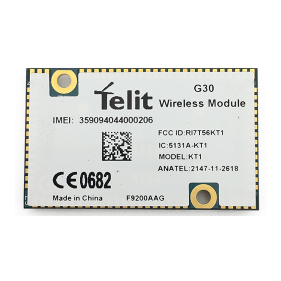
Page 23: General Product Description
The G30 series was designed for Zero time, Zero effort integration, getting you to market faster than ever. The G30 features both an 81 pin LGA interface form factor and an optional 70-pin B2B connector for various design possibilities. The optional connectorized platform maintains the same mounting design as the award winning G24 module, so you can leverage the G30’s rich feature set but remain with your connectorized design. - Page 24 G30 Hardware User Guide 1VV0300919 Rev.0 – 2011-05-04 NOTE: Telit reserves the right to change the specifications without prior notice. Product Features Operating systems: GSM 850/GSM 900 DCS 1800/PCS 1900 Physical Characteristics Size (with 3 mm connector): 24.4x40x.3.5mm Ø Mounting: SMT (LGA module) or two 2.4 mm holes (70 pin connector...
- Page 25 G30 Hardware User Guide 1VV0300919 Rev.0 – 2011-05-04 Connectivity: UART: BR from 2400 bps to 230400 bps Auto BR up to 230400 bps C (Master, M2M Zone only): I2S or SPI (Master data logging only, AT command selection) RTC supply:...
- Page 26 G30 Hardware User Guide 1VV0300919 Rev.0 – 2011-05-04 DTMF support Audio control: Echo canceller, noise reduction, side tone and gain control, Tx / Rx digital filter control GSM Supplementary Service Call Hold/Resume (CH) Call Waiting (CW) Multi-Party (MTPY) Call Forwarding (CF)
-
Page 27: Regulatory And Approvals
UCS2 coded, the rest of commands or responses, remains in IRA alphabet AT Command Set GSM 07.05 GSM 07.07 Legacy Motorola proprietary AT commands Table 2-1: G30 Product Specifications 2.2. Regulatory and Approvals • R&TTE • GCF • FCC/IC • PTCRB •... -
Page 28: European Union Directives Conformance Statement
The above gives an example of a typical Product Approval Number. IMPORTANT: The following paragraphs must be addressed by the integrator to ensure their host is in compliance to the G30 FCC grant and/or the FCC grant of the host device. 2.2.2. CFR 47 Part 15.19 specifies label requirements The following text may be on the product, user's manual, or container. - Page 29 G30 Hardware User Guide 1VV0300919 Rev.0 – 2011-05-04 turning the equipment off and on, the user is encouraged to try to correct the interference by one or more of the following measures: - Reorient or relocate the receiving antenna. - Increase the separation between the equipment and receiver.
-
Page 30: Hardware Interface Description
G30 module. 3.1. Architecture Overview The figure below illustrates the primary functional components of the G30. Figure 3-1: G30 Block Diagram Reproduction forbidden without written authorization from Telit Communications S.p.A. - All Rights Reserved. Page 30 of 104... -
Page 31: Baseband
70 pin connector interface. 3.1.2. RF Block The G30 RF section is designed with minimum discrete parts, making it more reliable. The RF block consists of: • RF Transceiver/Receiver block in the same single chip IC as the MCU • 2 Rx Filters •... -
Page 32: Table 3-1: G30 Operating Modes
Any signals connected to the interface connector must be set tri-state. RTC Mode Valid VRTC supply. The G30 Interfaces are Off. Only the internal VCC supply is disconnected. RTC timer is operating. Any signals connected to the interface connector must be set tri-stated. -
Page 33: Power Supply
3.3. Power Supply The G30 power supply must be a single external DC voltage source of 3.3V to 4.2V. The power supply must be able to sustain the voltage level during a GSM transmit burst current surge, which may reach 2.0A. -
Page 34: Power Consumption
To minimize the losses and transients on the power supply lines, it is recommended to follow these guidelines: • Use a 1000 uF, or greater, low ESR capacitor on the G30 supply inputs. The capacitor should be located as near to the G30 interface connector as possible. -
Page 35: Power On/Off Operation
RESET_IN, and the output signal CTS. The RESET_IN is usually an input signal to the G30, and its main function is to initiate HW reset to the G30. However, this signal can also serve as "live indication" signal, and indicate whether G30 is powered on or off. -
Page 36: Power Supply Turn-On
Asserting the PWR_ON signal low for a minimum of 600 milliseconds (0.6 seconds) and a maximum of 1.5 seconds will cause the G30 to turn-on. Asserting the PWR_ON signal low for more than 1.5 seconds may cause the G30 to interpret the signal as a power-off command, and turn off immediately after turning on. -
Page 37: Turning The G30 Off Using Pwr_On
3.5.1. Activating Low Power Mode By default, the G30 powers on in Idle mode. In this mode the G30 interfaces and features are functional and the module is fully active. Low power mode is activated by the ATS24 command. The value set by this command determines the inactive state duration required by G30, in seconds, after which G30 will enter sleep mode. -
Page 38: Serial Interface During Low Power Mode
Figure 3-6: ATS24 Operation IMPORTANT: G30 will not enter low power mode in any case when there is data present on the serial interface or incoming from the GSM network or an internal system task is running. Only when processing of any external or internal system task has completed, and G30 is inactive for the duration of ATS24, it will enter low power mode. -
Page 39: Terminating Low Power Mode
G30 from low power mode and switch to Idle mode. G30 will remain in Idle mode, awake and fully active, as long as WKUPI signal remains low. When this signal is disabled and set high again, G30 will return to Sleep mode automatically, according to the ATS24 settings (see the following figure). -
Page 40: Figure 3-9: Serial Interface Data
It provides the application full control of the G30 operating mode and guarantees that data on the serial interface will not be lost or misinterpreted. The WKUPI signal must be used to wake up G30 from low power mode if the serial interface has been disabled by the AT+MSCTS command. -
Page 41: Real Time Clock
When the power supply is disconnected from G30 and no voltage is supplied to the VRTC pin, the RTC timer will reset and the current time and date will be lost. On the next G30 power-up the time and date will need to be set again automatically or manually. -
Page 42: Figure 3-10: Uart Interface Signals
IMPORTANT: The G30 UART will not send data over the serial interface in case the DTR and/or RTS input signals are disabled (set high). Therefore, regardless of the handshake method, it is still required to enable these signals for proper operation, by asserting them low. -
Page 43: Serial Peripheral Interface (Spi)
Serial Peripheral Interface (SPI) The G30 provides a synchronous SPI-compatible serial interface, used for data logging only, implemented with the synchronous serial controller hardware block of the G30. The SPI is a master-slave protocol: the module runs as a SPI master device. -
Page 44: Flashing And Data Logging
In the event of logging or reflashing the module SW, the host must provide access to several I/O lines especially when using the 81 pin LGA interface version. The G30 SPI interface is used for data logging, and therefore, it is recommended that the host application will have the ability to support it. - Page 45 G30 Hardware User Guide 1VV0300919 Rev.0 – 2011-05-04 header connector that will contain all required signals with additional SPI indication, VCC and GND signals. NOTE: When a header can’t be implemented due to engineering constrains (lack of place), the host application should support sufficient soldering pads or test points for wire-up.
-
Page 46: I 2 C Bus Interface
The module provides an I C bus interface which includes a serial data line and a clock line on the board to board pins. The G30 I C acts as master only. The I C bus interface is available to the user only with M2M Zone Platform. -
Page 47: Sim Interface
Both 1.8 V and 3 V SIM types are supported; activation and deactivation with automatic voltage switch from 1.8 V to 3 V is implemented. G30 is designed to support two SIM card options with the same SIM signals: External SIM card, or an on board Embedded SIM (eSIM), depending on the G30 model. -
Page 48: 1Vv0300919 Rev.0 - 2011-05-04
SIM. G30 supports dynamic detection of the SIM card, through a dedicated SIM detection signal. G30 will detect a SIM card insertion or removal upon power up or during operation by the transitions on the SIM_PD_N signal. -
Page 49: Embedded Sim
The eSIM main advantage is it robustness, making it an ideal solution for the M2M, and automotive application. Since an eSIM is actually an IC soldered on the G30, it can withstand wider temperature range than a regular external SIM card that is usually made of plastic, and gets twisted and bowed at high temperature, causing disconnection inside the SIM tray. -
Page 50: Audio Interface
3.9.1. Handset Microphone Port The handset microphone port is the G30 power-up default active audio input for voice calls. It is located on pin 51 at the G30 81 pin LGA interface, named MIC. It is designed as a single-ended input and should be referenced to the G30 analog ground. -
Page 51: Headset Microphone Port
The headset microphone port is designed for use with, but not limited to, a headset audio device. It is located at pin 53 on the G30 81 pin LGA interface, named MIC_HDST. Reproduction forbidden without written authorization from Telit Communications S.p.A. - All Rights Reserved. Page 51 of 104... -
Page 52: Table 3-10: Headset Microphone Port Specifications
G30 Hardware User Guide 1VV0300919 Rev.0 – 2011-05-04 It is designed as a single-ended input and should be referenced to the G30 analog ground. The microphone input includes all the necessary circuitry to support a direct connection to a headset microphone device. It incorporates an internal bias voltage of 2.0V through a 3.0kΩ... -
Page 53: Differential Speaker (Handset) Port
Differential Speaker (Handset) Port The analog differential speaker port is the G30 power-up default active output for voice calls and DTMF tones. It is located at pins 48 and 49 on the G30 81 pin LGA interface, named SPKR_N and SPKR_P respectively. -
Page 54: Mono Speaker (Headset) Port
The mono speaker port can be used for voice calls and DTMF tones. It is located at pin 47 on the G30 81 pin LGA interface, named HDST_SPK. It is designed as a single-ended output with 32Ω impedance, referenced to the G30 analog ground. -
Page 55: Headset Detection
3.9.5. Headset Detection The G30 operates by default in the basic audio mode with the differential speaker (handset) audio path, for DTMF tones, speech, rings, and alert tones active. The headset (mono speaker) path is an alternate audio path in basic mode. It is designed for, but not limited to, a personal hands-free audio device, a headset, using the headset microphone input device and the headset speaker output device. -
Page 56: Digital Audio Interface
2's compliment coding. G30 is the PCM bus master, supplying the clock and sync signals to the application. The G30 digital interface is a 4 signal PCM bus, which includes a bit clock output signal for the bus timing, a frame sync output signal for audio sampling timing, and serial data input and output signals. -
Page 57: Operating Modes
Figure 3-21: Voiceband Mode PCM Bus Coding Format 3.9.8. Operating Modes The G30 audio interface includes 2 modes of operation. Each operating mode defines the audio input and output devices to be used for each audio sound type and their programmable settings. -
Page 58: Table 3-14: Basic Mode Audio Paths
3.9.8.2. Advanced Mode Advanced audio mode utilizes G30's unique set of AT commands for advanced audio programming. The expanded AT command set enables to define a specific audio path and setting, which are not part of the default configuration, for each type of audio sound (speech, DTMF tones, rings and alerts). -
Page 59: Audio Programming Interface
Table 3-15: Advanced Mode Commands 3.9.9. Audio Programming Interface The G30 incorporates a unique audio programming interface, through AT commands, which controls the following audio features: • Audio Path - Defines the input and output devices for speech, DTMF tones, rings and alerts. -
Page 60: Audio Design
G30 Hardware User Guide 1VV0300919 Rev.0 – 2011-05-04 The G30 also supports full rate (FR), half rate (HR), enhanced full rate (EFR) and adaptive multi-rate (AMR) speech coding algorithms, which are used by the GSM network. These algorithms are configured and operated by the GSM network provider. -
Page 61: A/D Interface
The G30 includes 3 Analog to Digital Converter (ADC) signals with 12-bit resolution, for environmental and electrical measurements. The ADC signals measure an analog DC voltage level on their inputs which is converted to a 12-bit digital value for further processing by G30 or the user application. -
Page 62: Power Supply A/D
In case the defined periodical measurement rate is equal to, or shorter than, the defined sleep mode delay settings (ATS24), G30 will not enter low power mode. Applying voltage to ADC lines before power up is forbidden and may cause G30 power up issues. -
Page 63: Controls And Indicators Interface
Table 3-19: GPAD Specifications 3.11. Controls and Indicators Interface The G30 incorporates several interface signals for controlling and monitoring the module's operation. The following paragraphs describes these signals and their operation. The following table gives a description of the controls and indicators signals. - Page 64 G30 Hardware User Guide 1VV0300919 Rev.0 – 2011-05-04 Pin # Pin # (81 pin (70 pin Function Remarks connector Signal Name interface) interface) Wake-Up Out voltage domain. Output driver class F. PU/PD class B. WKUPI Interrupt Generic digital interfaces voltage domain.
-
Page 65: Reset
3.11.2. VREF Reference Regulator The G30 incorporates a regulated voltage output, VREF. The regulator provides a 2.85V output for use by the customer application. This regulator can source up to 30 mA of current to power any external digital circuits. -
Page 66: Vrtc
3.11.3. VRTC The G30 incorporates a real time block and is operated by the VRTC power located on pin 62 of the 81-pin LGA interface, or pin 60 of the 70-pin connector interface. For detailed explanation, refer to “Real Time Clock”. -
Page 67: Antenna Detection
Figure 3-23: WKUPO Operation The following guidelines apply to the wakeup-out mechanism: • G30 will set the WKUPO signal low to indicate that in has data to send through the serial interface. • G30 will start sending the data to the application after the delay defined by ATS102. -
Page 68: Gprs Detection
3.11.7. General Purpose I/O The G30 incorporates 9 general purpose IO signals in the 81 pin LGA interface, or 8 general purpose IO signals in the 70 pin connector interface for the user application. Each GPIO signal may be configured and controlled by AT command. These signals may be used to control or set external application circuits, or to receive indications from the external application. -
Page 69: Specifications
G30 Hardware User Guide 1VV0300919 Rev.0 – 2011-05-04 65,67 RF isolated Ground Route Ground according “RF Recommendation” on page 80 RF Antenna (U.FL 50Ω nominal impedance. connector) (Applicable for G30 with U.FL connector model) CAUTION: A RF keepout area exists near the RF ANT pad of the LGA interface. Verify this area is left in-routed. -
Page 70: Table 3-22: Antenna Interface Specifications
Table 3-22: Antenna Interface Specifications It is the Integrator's responsibility to design the antenna or antenna assembly used with the G30. This will highly affect the RF performance of the G30 (dropped calls, battery consumption etc.). The following guidelines should be followed: •... -
Page 71: Electrical And Environmental Specifications
1VV0300919 Rev.0 – 2011-05-04 Electrical and Environmental Specifications 4.1. Absolute Maximum Ratings The following table gives the maximum electrical characteristics of the G30 interface signals. CAUTION: Exceeding the values may result in permanent damage to the module. Limit Values Description... -
Page 72: Operating Parameters
G30 Hardware User Guide 1VV0300919 Rev.0 – 2011-05-04 4.2. Operating Parameters 4.2.1. Supply/power Pins Limit Values Supply Description Name Module Supply 3.3 V 3.8 V 4.2 V RTC Supply VRTC 1.86 V 2.0 V 2.14 V Table 4-2: Input Characteristics... -
Page 73: Digital Pins
G30 Hardware User Guide 1VV0300919 Rev.0 – 2011-05-04 4.2.2. Digital Pins Limit Values Voltage Domain Parameter Unit Remarks Voltage Domain = L-level input -0.20 0.55 VIO = 2.85 V Generic digital interfaces Voltage Domain = H-level input 2.05 3.30 VIO = 2.85 V... - Page 74 G30 Hardware User Guide 1VV0300919 Rev.0 – 2011-05-04 Limit Values Voltage Domain Parameter Unit Remarks L-level output for output 0.00 0.80 = +15.0 mA driver class B slow L-level output for output 0.00 0.35 = +5.0 mA driver class B...
-
Page 75: Table 4-5: Output Characteristics
G30 Hardware User Guide 1VV0300919 Rev.0 – 2011-05-04 Voltage Domain Parameter Unit Remarks Limit Values H-level output for output 2.05 2.85 = -1.5 mA driver class E and F C interface L-level output 0.00 0.40 = +3.0 mA VSIM = 1.80 V 0.00... -
Page 76: Table 4-6: Pad Pull-Up And Pull-Down Characteristics
G30 Hardware User Guide 1VV0300919 Rev.0 – 2011-05-04 Limit Values Voltage Domain Parameter Unit Remarks Pull-up input current for pull -450 class A Pull-up input current for pull -100 class B Pull-up input current for pull class C Generic digital... -
Page 77: Audio Pins
G30 Hardware User Guide 1VV0300919 Rev.0 – 2011-05-04 4.2.3. Audio Pins Limit Values Parameter Unit Remarks Differential input voltage 1.03 Differential input impedance kΩ Input capacitance Signal to distortion Gain stage = +12dB Bandwidth = 300-3900Hz (GSM mode) Signal-to-noise ratio... -
Page 78: Table 4-7: Audio Transmit Path Characteristics
G30 Hardware User Guide 1VV0300919 Rev.0 – 2011-05-04 Parameter Unit Remarks Limit Values Cut-off frequency of anti-alias filter Variation due to change in Absolute gain drift ±2 supply, temperature and life time. Table 4-7: Audio Transmit Path Characteristics Limit Values... -
Page 79: Table 4-9: G30 Low Power Single-Ended Audio Receive Path Characteristics
Variation due to change in Absolute gain drift ±2 supply, temperature and life time. Table 4-9: G30 Low Power Single-ended Audio Receive Path Characteristics Reproduction forbidden without written authorization from Telit Communications S.p.A. - All Rights Reserved. Page 79 of 104... -
Page 80: Adc Pins
Signal to noise Input signal = 0dBFS, Code 0, A-weighted Signal to distortion Load = 8Ω, 350mW Power supply rejection 1kHz Table 4-10: G30 High Power Differential Audio Receive Path Characteristics 4.2.4. ADC Pins Limit Values Parameter Unit Remarks Resolution... -
Page 81: Environmental Specifications
Input leakage current Table 4-11: Input Characteristics 4.3. Environmental Specifications The following table gives the environmental operating conditions of the G30 module. Reproduction forbidden without written authorization from Telit Communications S.p.A. - All Rights Reserved. Page 81 of 104... -
Page 82: Application Interface Specifications
IMPORTANT: Interface signals that are not used by the customer application must be left unconnected. G30 incorporates the necessary internal circuitry to keep unconnected signal in their default state. Do not connect any components to, or apply any voltage on, signals that are not used by the application. -
Page 83: Figure 4-1: G30 - 70 Pin Connector Quick Integration Connections
G30 Hardware User Guide 1VV0300919 Rev.0 – 2011-05-04 Figure 4-1: G30 - 70 Pin Connector Quick Integration Connections Reproduction forbidden without written authorization from Telit Communications S.p.A. - All Rights Reserved. Page 83 of 104... -
Page 84: Figure 4-2: G30 - 81 Pin Lga Interface Quick Integration Connections
G30 Hardware User Guide 1VV0300919 Rev.0 – 2011-05-04 Figure 4-2: G30 - 81 Pin LGA Interface Quick Integration Connections Refer to “Interface Connector Specifications” on page Note: Pin No. (81 pin @70 Pin Value @ Characteristics Name Function Conn. Reset... - Page 85 G30 Hardware User Guide 1VV0300919 Rev.0 – 2011-05-04 Pin No. (81 pin @70 Pin Value @ Characteristics Name Function Conn. Reset (Operating Parameters) interface) Generic digital interfaces (Typ. 2.85V) voltage domain. GPIO7 GPIO Output driver class F. 100K PU PU/PD class B.
- Page 86 G30 Hardware User Guide 1VV0300919 Rev.0 – 2011-05-04 Pin No. (81 pin @70 Pin Value @ Characteristics Name Function Conn. Reset (Operating Parameters) interface) L - Valid GPRS connectio GPRS H - No GPRS connectio Not Connected RTC interface. (2.0V typ.)
- Page 87 G30 Hardware User Guide 1VV0300919 Rev.0 – 2011-05-04 Pin No. (81 pin @70 Pin Value @ Characteristics Name Function Conn. Reset (Operating Parameters) interface) Not Connected External reset signal RESET_IN External reset input voltage domain. Use OC circuit only 19K PU...
- Page 88 G30 Hardware User Guide 1VV0300919 Rev.0 – 2011-05-04 Pin No. (81 pin @70 Pin Value @ Characteristics Name Function Conn. Reset (Operating Parameters) interface) Generic digital interfaces (Typ. 2.85V) voltage domain. Data Set Ready Output driver class B slow. PU/PD class A.
- Page 89 G30 Hardware User Guide 1VV0300919 Rev.0 – 2011-05-04 Pin No. (81 pin @70 Pin Value @ Characteristics Name Function Conn. Reset (Operating Parameters) interface) High power 65,69 Used in ring tones or SPKR_P differential in hands free mode analog audio output Generic digital interfaces (Typ.
- Page 90 G30 Hardware User Guide 1VV0300919 Rev.0 – 2011-05-04 Pin No. (81 pin @70 Pin Value @ Characteristics Name Function Conn. Reset (Operating Parameters) interface) SIM interface voltage domain. SIM_PD_n SIM present detect OD/L Output driver class E. PU/PD class B.
-
Page 91: Table 4-13: Interface Specifications
G30 Hardware User Guide 1VV0300919 Rev.0 – 2011-05-04 Pin No. (81 pin @70 Pin Value @ Characteristics Name Function Conn. Reset (Operating Parameters) interface) 1,2,3,4 GND pins are internally Ground shorted between them. 1,2,3,4 GND pins are internally Ground shorted between them. -
Page 92: Mechanical Specifications
Mechanical Specifications 5.1. Board Dimensions The following pictures describe the G30 mechanical characteristics. Figure 5-1: G30 Mechanical Characteristics - 81 Pin LGA Interface Reproduction forbidden without written authorization from Telit Communications S.p.A. - All Rights Reserved. Page 92 of 104... -
Page 93: Figure 5-2: G30 Mechanical Characteristics - B2B Connector (70 Pin)
G30 Hardware User Guide 1VV0300919 Rev.0 – 2011-05-04 Figure 5-2: G30 Mechanical Characteristics - B2B Connector (70 Pin) Reproduction forbidden without written authorization from Telit Communications S.p.A. - All Rights Reserved. Page 93 of 104... -
Page 94: Lga Tape & Reel Specification
G30 Hardware User Guide 1VV0300919 Rev.0 – 2011-05-04 5.2. LGA Tape & Reel Specification The following picture shows LGA Tape & Reel specification. Each reel contains 500 units. Figure 5-3: LGA Tape & Reel Specification Reproduction forbidden without written authorization from Telit Communications S.p.A. - All Rights Reserved. Page 94 of 104... -
Page 95: Interface Connector Specifications
G30 Hardware User Guide 1VV0300919 Rev.0 – 2011-05-04 5.3. Interface Connector Specifications The G30 uses a single 70-pin, 0.5 mm pitch, board to board connector for the application interface. G30 interface connector option G30 Connector Mating Connector Stacking Height Molex 53748-0708 Molex 52991-0708 3.0 mm... -
Page 96: Mating Connector
G30 interface connectors, which are described in table 5-1. The following figure provides a reference drawing of the mating connectors mechanical dimensions. Figure 5-4: Mating Connector Dimensions For more information on the G30 mating connector, please refer to the Molex web site at http://www.molex.com/molex/index.jsp. 5.4. U.FL Connector Specifications The G30 uses a standard U.FL receptacle connector for the radio interface. -
Page 97: Figure 5-5: U.fl Connector Dimensions
G30 Hardware User Guide 1VV0300919 Rev.0 – 2011-05-04 Figure 5-5: U.FL Connector Dimensions The following table describes the U.FL connector characteristics. Parameter Specifications Characteristic Impedance 50 Ohms Frequency Range DC to 6 GHz 1.30 max DC to 3 GHz VSWR (mated pair) 1.40 max 3 to 6 GHz (cable dependent) -
Page 98: Mating Connector
The RF mating connector should be a standard U.FL plug connector or cable assembly, which corresponds to the G30 U.FL connector specifications. Only Hirose U.FL mating cable may be mated with G30. A family of Hirose mating cables are available. -
Page 99: Layout Recommendation
The following picture depicts the G30 mounting area. Figure 5-7: G30 Mounting Area The holes are used for mechanical mounting of G30 to the application board but also for grounding support. Using conductive elements to install G30, significantly improves the overall grounding of the module and therefore improves the G30 performance and stability. -
Page 100: Soldering Footprint
G30 Hardware User Guide 1VV0300919 Rev.0 – 2011-05-04 5.6.1. Soldering Footprint The following figure gives a layout recommendation for the G30. Figure 5-8: G30 Soldering Footprint (Top View) Routing signals other then GND (Ground) within inner soldering footprint area of •... -
Page 101: Soldering Re-Flow
Cover all Pads area with inner GND Layer below the 0.45mm routing clearance. • 5.7. Soldering Re-flow G30 LGA recommended soldering re-flow process is given in thefollowing table and picture. Classification of regular Pb-Free Assembly Re-flow Profile Preheat and Soak Temperature minimum (Tsmin) 150°C... - Page 102 G30 Hardware User Guide 1VV0300919 Rev.0 – 2011-05-04 NOTE: Any G30 LGA removal must be performed according to IPC-7711 standard "Rework of Electronic Assemblies" chap 3.9.1 or 3.9.2 regarding “BGA/CSP Removal”. The IPC- 7711 can be found at www.ipc.org. Reproduction forbidden without written authorization from Telit Communications S.p.A. - All Rights Reserved. Page 102 of 104...
-
Page 103: Acronyms And Abbreviations
G30 Hardware User Guide 1VV0300919 Rev.0 – 2011-05-04 Acronyms and abbreviations Adaptive Multi Rate Advice of Charge Board to Board Baud Rate Bits Per Second Circuit Switched Data Clear to Send Data Carrier Detect Data Communication Equipment (such as modems) -
Page 104: Document History
G30 Hardware User Guide 1VV0300919 Rev.0 – 2011-05-04 Mobile Terminated Original Equipment Manufacturer Printed Circuit Board Power Class Level Pulse Code Modulation Personal Communication System (also known as GSM 1900) Pull Down Personal Data Assistant Packet Data Unit Phase-locked Loop...
Need help?
Do you have a question about the G30 and is the answer not in the manual?
Questions and answers