Table of Contents
Advertisement
Quick Links
www.ti.com
EVM User's Guide: DLPLCRC410EVM, DLPLCR65NEVM,
DLPLCR70EVM, DLPLCR70UVEVM, DLPLCR95EVM,
DLPLCR95UVEVM
®
DLP
Discovery™ 4100 Development Platform
Description
The DLPLCRC410EVM, paired with one of five
other DMD-based EVMs, is an evaluation platform
exhibiting advanced light control for applications like
lithography, 3D Printing (SLS and SLA), Machine
Vision, and Marking and Coding. This EVM enables
evaluations of new customer illumination sources,
optics, algorithm, and exposure processes to quicken
potential evaluation of DLP technology, customer
learning cycles, and times to market.
DLPU040C – OCTOBER 2016 – REVISED JULY 2024
Submit Document Feedback
Features
•
Light control of one of 5 different DMDs
•
Binary pattern rates up to 32kHz
•
Grayscale patterns rates up to 1.9kHz
•
2xLVDS DDR input data interface at 400Mhz clock
rate
•
Supports random row addressing of DMD rows
DLPLCRC410EVM
Copyright © 2024 Texas Instruments Incorporated
®
DLP
Discovery™ 4100 Development Platform
Description
1
Advertisement
Table of Contents

Related Manuals for Texas Instruments DLPLCRC410EVM


Summary of Contents for Texas Instruments DLPLCRC410EVM
-
Page 1: Description
DLPLCR70EVM, DLPLCR70UVEVM, DLPLCR95EVM, DLPLCR95UVEVM ® Discovery™ 4100 Development Platform Description Features The DLPLCRC410EVM, paired with one of five • Light control of one of 5 different DMDs other DMD-based EVMs, is an evaluation platform • Binary pattern rates up to 32kHz exhibiting advanced light control for applications like •... -
Page 2: Table Of Contents
List of Figures Figure 1-1. D4100 Platform Diagram............................6 Figure 1-2. DLPLCRC410EVM connected to DLPLCR95EVM....................Figure 2-1. DLPLCRC410EVM Controller Board Key Components.................... Figure 2-2. DLPLCRC410EVM Controller Connectors (Top View).................... Figure 2-3. DLPLCRC410EVM Controller Connectors (Bottom View)..................Figure 2-4. DLPLCRC410EVM Controller Configuration Jumpers.................... - Page 3 Table 2-18. Shared USB Signal Enable/Disable........................26 Table 2-19. DLPA200 B Output Enable............................26 Table 2-20. SW1 Dip Switch Assignments..........................27 Table 2-21. DLPLCRC410EVM Test Point Net Names......................29 Table 3-1. DMD Characteristics..............................Table 3-2. SW1 Dip Switch Assignments...........................54 ® DLPU040C – OCTOBER 2016 – REVISED JULY 2024 Discovery™...
-
Page 4: Evaluation Module Overview
DLPLCRC410EVM controller board. The DLPLCRC410EVM board includes the DLPC410, DLPR410, DLPA200, digital receiver, flash, power management circuits, and supporting digital logic. To give designers scalability to port the DLP design work across multiple DMD devices, the DLPLCRC410EVM operates with any of the following five DMD EVMs: •... -
Page 5: Table 1-1. D4100 Platform Evms And Dmd
Evaluation Module Overview When the DLPLCRC410EVM is connected to any of the DMD EVMs, the DLPC410, Applications FPGA, and Software GUI recognizes and provides the proper signals and timing to the attached DMD. Out of the box, the DLPLCRC410EVM delivers a small set of scrolling test patterns, which allow customers to evaluate the optical designs for related optical performance. -
Page 6: Figure 1-1. D4100 Platform Diagram
64 Bit SODIMM Connector * DLPLCR95(UV)EVMs only Figure 1-1. D4100 Platform Diagram The DLP Discovery 4100 EVM Controller Board of the DLPLCRC410EVM contains: • DLPC410 DLP Digital Controller – Provides input high speed 16/32/64 bit 2xLVDS data and control user interface. - Page 7 – Mictor test connectors for logic analyzer connection. – JTAG headers for device programming. – GPIO connectors for general purpose digital I/O. ® DLPU040C – OCTOBER 2016 – REVISED JULY 2024 Discovery™ 4100 Development Platform Submit Document Feedback Copyright © 2024 Texas Instruments Incorporated...
-
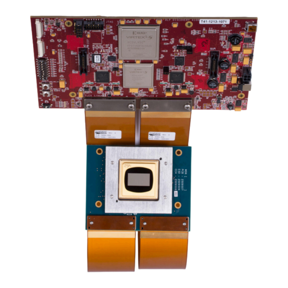
Page 8: Figure 1-2. Dlplcrc410Evm Connected To Dlplcr95Evm
Figure 1-2. Other DMD EVMs connect to the DLPLCRC410EVM in a similar fashion and look very similar, except the DLPLCRC410EVM only uses a single flex cable (Flex 1) for connection between the Controller Board and the DMD Board. Figure 1-2. DLPLCRC410EVM connected to DLPLCR95EVM ®... -
Page 9: Hardware
Mictor Mictor Battery Figure 2-1. DLPLCRC410EVM Controller Board Key Components 2.1.1 Xilinx Virtex 5 APPSFPGA The APPSFPGA (Xilinx Virtex 5 LX50) is used for development of interface and control designs for the DMD. The APPSFPGA is connected to a number of I/O connectors, interface controllers, and memory for use in prototyping a custom control design prior to developing a custom board designs. - Page 10 2.1.12.1 J12 Power Connector The J12 power connector is the input power supply connector for the DLPLCRC410EVM controller board. For proper operation, this power connector must be connected to a 5 VDC power supply capable of providing 30 W of input power.
-
Page 11: Hardware Overview And Setup
The following steps must be followed in starting board operation using the default APPSFPGA code installed at the factory: 1. Connect the desired DMD EVM to the DLPLCRC410EVM using the provided flex cables. A single flex cable connects J13 to either the DLPLCR70EVM, DLPLCR70UVEVM, or the DLPLCR65NEVM. Two flex cables attached to J13 and J14 are used for the DLPLCR95EVM and DLPLCR95UVEVM. -
Page 12: Figure 2-2. Dlplcrc410Evm Controller Connectors (Top View)
J12, J18 Input Power Connectors DLPC410 Mictor Connector J13, J14 DMD Flex Connectors Figure 2-2. DLPLCRC410EVM Controller Connectors (Top View) J16 EXP1 J17 EXP2 J15 DDR2 SODIMM Figure 2-3. DLPLCRC410EVM Controller Connectors (Bottom View) ® Discovery™ 4100 Development Platform DLPU040C – OCTOBER 2016 – REVISED JULY 2024 Submit Document Feedback Copyright ©... -
Page 13: Table 2-1. J12 Input Power Pinout
Pin Name 3.3V USB_GPIO B3 USB_GPIO B7 USB_GPIO B2 USB_GPIO B6 USB_GPIO B1 USB_GPIO B5 USB_GPIO B0 USB_GPIO B4 ® DLPU040C – OCTOBER 2016 – REVISED JULY 2024 Discovery™ 4100 Development Platform Submit Document Feedback Copyright © 2024 Texas Instruments Incorporated... -
Page 14: Table 2-5. J6 Gpio_A Connector
AF12 ECP2_M_TP24 ECP2_M_TP13 AE11 ECP2_M_TP23 ECP2_M_TP14 ECP2_M_TP22 ECP2_M_TP15 AF11 ECP2_M_TP21 ECP2_M_TP16 AB12 ECP2_M_TP20 ECP2_M_TP17 AA16 ECP2_M_TP19 ECP2_M_TP18 AD13 ® Discovery™ 4100 Development Platform DLPU040C – OCTOBER 2016 – REVISED JULY 2024 Submit Document Feedback Copyright © 2024 Texas Instruments Incorporated... -
Page 15: Table 2-7. J9 Usb/Appsfpga Mictor Connector
USB_FD11/ USB_CTRL2/ TST_HDR_BY1_3 TST_HDR_BY3_3 USB_FD12/ USB_CTRL3/ TST_HDR_BY1_4 TST_HDR_BY3_4 USB_FD13/ USB_FPGA_RESET/ TST_HDR_BY1_5 TST_HDR_BY3_5 USB_FD14/ USB_INT5/ TST_HDR_BY1_6 TST_HDR_BY3_6 USB_FD15/ TST_HDR_BY1_7 ® DLPU040C – OCTOBER 2016 – REVISED JULY 2024 Discovery™ 4100 Development Platform Submit Document Feedback Copyright © 2024 Texas Instruments Incorporated... - Page 16 DDC_DOUT_A0_DPP DDC_DOUT_A0_DPN SCPDI DMD_A_RESET DMDSPARE0 MBRST1_11 MBRST1_5 MBRST1_4 MBRST1_0 MBRST1_3 MBRST1_2 MBRST1_8 DDC_DOUT_B0_DPP DDC_DOUT_B0_DPN DDC_DOUT_B2_DPP DDC_DOUT_B2_DPN DDC_DOUT_B4_DPP DDC_DOUT_B4_DPN ® Discovery™ 4100 Development Platform DLPU040C – OCTOBER 2016 – REVISED JULY 2024 Submit Document Feedback Copyright © 2024 Texas Instruments Incorporated...
-
Page 17: Table 2-8. J13 Dmd Flex Connector 1
Pin Number Pin Name DDC_DOUT_B6_DPP DDC_DOUT_B6_DPN DDC_SCTRL_B_DPP DDC_SCTRL_B_DPP DDC_DOUT_B8_DPP DDC_DOUT_B8_DPN DDC_DOUT_B10_DPP DDC_DOUT_B10_DPN DDC_DOUT_B12_DPP DDC_DOUT_B12_DPN DDC_DOUT_B14_DPP DDC_DOUT_B14_DPN 3.3V 3.3V ® DLPU040C – OCTOBER 2016 – REVISED JULY 2024 Discovery™ 4100 Development Platform Submit Document Feedback Copyright © 2024 Texas Instruments Incorporated... - Page 18 DDC_DOUT_C0_DPP DDC_DOUT_C0_DPN SCPDI DMD_B_RESET DMDSPARE0 MBRST2_11 MBRST2_5 MBRST2_4 MBRST2_0 MBRST2_3 MBRST2_2 MBRST2_8 DDC_DOUT_D0_DPP DDC_DOUT_D0_DPN DDC_DOUT_D2_DPP DDC_DOUT_D2_DPN DDC_DOUT_D4_DPP DDC_DOUT_D4_DPN ® Discovery™ 4100 Development Platform DLPU040C – OCTOBER 2016 – REVISED JULY 2024 Submit Document Feedback Copyright © 2024 Texas Instruments Incorporated...
-
Page 19: Table 2-9. J14 Dmd Flex Connector 2
Pin Number Pin Name DDC_DOUT_D6_DPP DDC_DOUT_D6_DPN DDC_SCTRL_D_DPP DDC_SCTRL_D_DPP DDC_DOUT_D8_DPP DDC_DOUT_D8_DPN DDC_DOUT_D10_DPP DDC_DOUT_D10_DPN DDC_DOUT_D12_DPP DDC_DOUT_D12_DPN DDC_DOUT_D14_DPP DDC_DOUT_D14_DPN 3.3V 3.3V ® DLPU040C – OCTOBER 2016 – REVISED JULY 2024 Discovery™ 4100 Development Platform Submit Document Feedback Copyright © 2024 Texas Instruments Incorporated... -
Page 20: Table 2-10. J15 Ddr2 Sodimm Connector
DDR2_D44 DDR2_D41 DDR2_DQS5_N DDR2_DM5 DDR2_DQS5_P DDR2_D42 DDR2_D46 DDR2_D43 DDR2_D47 DDR2_D48 DDR2_D52 DDR2_D49 DDR2_D53 DDR2_CK1_P DDR2_CK1_N DDR2_DQ56_N DDR2_DQ56_P DDR2_DM6 ® Discovery™ 4100 Development Platform DLPU040C – OCTOBER 2016 – REVISED JULY 2024 Submit Document Feedback Copyright © 2024 Texas Instruments Incorporated... -
Page 21: Table 2-11. J16 Exp-1
AC32 EXP1_DIFF_21_N EXP1_DIFF_20 AB32 EXP1_SE_IO_32 EXP1_DIFF_31_P EXP1_DIFF_18 AF34 EXP1_SE_IO_33 EXP1_DIFF_31_N EXP1_DIFF_18 AE34 EXP1_DIFF_19_P AG32 EXP1_DIFF_16 EXP1_DIFF_19_N AH32 EXP1_DIFF_16 ® DLPU040C – OCTOBER 2016 – REVISED JULY 2024 Discovery™ 4100 Development Platform Submit Document Feedback Copyright © 2024 Texas Instruments Incorporated... -
Page 22: Table 2-12. J16 Exp-1 Power And Ground
126, 127, 128, 129, 130, 131, 132 85, 86, 91, 92, 97, 98, 103, 104, 109, 110, 115, 116 VCC_3P3V ® Discovery™ 4100 Development Platform DLPU040C – OCTOBER 2016 – REVISED JULY 2024 Submit Document Feedback Copyright © 2024 Texas Instruments Incorporated... -
Page 23: Table 2-13. J17 Exp-2 Connector
EXP2_DIFF_9_P EXP2_DIFF_8_P EXP2_DIFF_9_N EXP2_DIFF_8_N EXP2_DIFF_7_P EXP2_DIFF_6_P EXP2_DIFF_7_N EXP2_DIFF_6_N EXP2_DIFF_5_P EXP2_DIFF_4_P EXP2_DIFF_5_N EXP2_DIFF_4_N EXP2_DIFF_3_P EXP2_DIFF_2_P EXP2_DIFF_3_N EXP2_DIFF_2_N EXP2_DIFF_1_P EXP2_DIFF_0_P ® DLPU040C – OCTOBER 2016 – REVISED JULY 2024 Discovery™ 4100 Development Platform Submit Document Feedback Copyright © 2024 Texas Instruments Incorporated... -
Page 24: Table 2-14. J17 Exp-2 Power And Ground
Table 2-15. H1 Xilinx APPSFPGA JTAG Header H1 Pin Number Pin Name 1, 3, 5, 7, 9, 11, 13 P2P5V 12, 14 ® Discovery™ 4100 Development Platform DLPU040C – OCTOBER 2016 – REVISED JULY 2024 Submit Document Feedback Copyright © 2024 Texas Instruments Incorporated... -
Page 25: Figure 2-4. Dlplcrc410Evm Controller Configuration Jumpers
D4100 controller board. Figure 2-4. DLPLCRC410EVM Controller Configuration Jumpers 2.2.3.1 J2 – EXP Voltage Select J2 is used to select either 2.5V or 3.3V voltage supplies for the EXP bus FPGA banks. This setting needs to match the I/O voltage required by any board attached to the EXP connectors. -
Page 26: Figure 2-5. Dlplcrc410Evm On-Board Switches
Jumper Position DLPA200 B Outputs Disabled Enabled 2.2.4 Switches This section defines the function of the switches on the DLPLCRC410EVM Controller Board. Switches 1 through 4 locations are shown in Figure 2-5 Figure 2-5. DLPLCRC410EVM On-Board Switches ® Discovery™ 4100 Development Platform DLPU040C –... -
Page 27: Table 2-20. Sw1 Dip Switch Assignments
TI highly recommends to first Park the DMD micromirrors by pressing SW3. ® DLPU040C – OCTOBER 2016 – REVISED JULY 2024 Discovery™ 4100 Development Platform Submit Document Feedback Copyright © 2024 Texas Instruments Incorporated... -
Page 28: Figure 2-6. Dlplcrc410Evm Controller Board Indicators
Hardware www.ti.com 2.2.5 Power and Status LEDs This section describes indicators that verify proper function of the DLPLCRC410EVM Controller Board. Figure shows the controller board indicator locations. D3, D17 D16, D2 Figure 2-6. DLPLCRC410EVM Controller Board Indicators 2.2.5.1 D1 – USB Connection Indicator This LED is not used at this time. -
Page 29: Figure 2-7. Dlplcrc410Evm Test Point Locations
TP14 TP27 TP29 TP17 TP28 TP32 TP13 TP16 TP15 TP31 TP30 Figure 2-7. DLPLCRC410EVM Test Point Locations Table 2-21. DLPLCRC410EVM Test Point Net Names Test Point Net Name Test Point Net Name GROUND V5_DXP VCC_VREF V5_DXN GROUND RESET SCPDO BKPT... -
Page 30: Software
This chapter describes the operation of the DLP Discovery 4100 Explorer Graphical User Interface (GUI) software. The Discovery 4100 Explorer GUI provides control and display functions for the DLP Discovery 4100 Development Platform via the USB 2.0 interface to the DLPLCRC410EVM. Figure 3-1. Discovery 4100 Explorer GUI ®... -
Page 31: Overview
Descriptions of the Discovery 4100 Explorer menus, toolbars and display windows • Operation instructions 3.1.1 Software Overview The DLP Discovery 4100 Explorer GUI allows the user to control the DLPLCRC410EVM controller board hardware via USB 2.0 (or 1.1). The software uses the Discovery 4100 ActiveX ™ control API which is documented separately in the DLP®... -
Page 32: Dlp Discovery 4100 Operation
If there are no installation errors, then the following steps must be followed to operate the device: 1. Install the software by executing the file D4100Explorer-2.0-windows-installer.exe. Install the software BEFORE connecting the USB cable to the DLPLCRC410EVM Controller Board. The setup program installs the software and driver INF files necessary for operation. -
Page 33: Figure 3-3. Browse For Driver Software
7. Click Let me pick from a list of device drivers on my computer. Figure 3-4. Pick from a list of Device Drivers ® DLPU040C – OCTOBER 2016 – REVISED JULY 2024 Discovery™ 4100 Development Platform Submit Document Feedback Copyright © 2024 Texas Instruments Incorporated... -
Page 34: Figure 3-5. Select Universal Serial Bus Devices
8. Select Universal Serial Bus devices. Click Next. Figure 3-5. Select Universal Serial Bus devices 9. Click on Have Disk. Figure 3-6. Have Disk ® Discovery™ 4100 Development Platform DLPU040C – OCTOBER 2016 – REVISED JULY 2024 Submit Document Feedback Copyright © 2024 Texas Instruments Incorporated... -
Page 35: Figure 3-7. Browse For .Inf File
11. Click TI D4100 Explorer 12. Click Next. Figure 3-8. Select TI D4100 Explorer 13. Windows installs the driver. ® DLPU040C – OCTOBER 2016 – REVISED JULY 2024 Discovery™ 4100 Development Platform Submit Document Feedback Copyright © 2024 Texas Instruments Incorporated... -
Page 36: Figure 3-9. Driver Installation Window
15. Verify driver installation in Device Manager window as shown in Figure 3-10. Figure 3-10. Verify Device 16. Start the DLP Discovery Explorer GUI from the Start/Texas Instruments/DLP Discovery 4100 Explorer menu. ® Discovery™ 4100 Development Platform DLPU040C – OCTOBER 2016 – REVISED JULY 2024 Submit Document Feedback Copyright ©... -
Page 37: Figure 3-11. Discovery 4100 Explorer Usb And Dmd - Connection Status
DMD. The answer is to always restart the GUI software program after connecting to a different Discovery EVM. ® DLPU040C – OCTOBER 2016 – REVISED JULY 2024 Discovery™ 4100 Development Platform Submit Document Feedback Copyright © 2024 Texas Instruments Incorporated... -
Page 38: Graphical User Interface
The menu bar commands provide standard menu access to software commands as shown in Figure 3-13. Figure 3-13. Menu Bar ® Discovery™ 4100 Development Platform DLPU040C – OCTOBER 2016 – REVISED JULY 2024 Submit Document Feedback Copyright © 2024 Texas Instruments Incorporated... -
Page 39: Figure 3-14. File Menu
3.3.1.3 DMD Menu The DMD menu is used to select the DLPC410 Control operation mode. Figure 3-16. DMD Menu ® DLPU040C – OCTOBER 2016 – REVISED JULY 2024 Discovery™ 4100 Development Platform Submit Document Feedback Copyright © 2024 Texas Instruments Incorporated... -
Page 40: Figure 3-17. Execution Menu
• Set End – Sets the end point of command execution within the script. Figure 3-17. Execution Menu ® Discovery™ 4100 Development Platform DLPU040C – OCTOBER 2016 – REVISED JULY 2024 Submit Document Feedback Copyright © 2024 Texas Instruments Incorporated... -
Page 41: Figure 3-18. Test Patterns Menu
The Help menu contains a link to standard Windows help file contents and the command to load the About dialog box. Figure 3-19. Help Menu ® DLPU040C – OCTOBER 2016 – REVISED JULY 2024 Discovery™ 4100 Development Platform Submit Document Feedback Copyright © 2024 Texas Instruments Incorporated... -
Page 42: Figure 3-20. Toolbar
Set Start and Set End icons set the start point and end point of command execution within a script. 3.3.2.4 Help Button The Help button displays the help contents for the application. ® Discovery™ 4100 Development Platform DLPU040C – OCTOBER 2016 – REVISED JULY 2024 Submit Document Feedback Copyright © 2024 Texas Instruments Incorporated... -
Page 43: Figure 3-21. Script Commands Window
Once you’ve selected the commands and options, click the Add button to add the command options to the script. Figure 3-21. Script Commands Window ® DLPU040C – OCTOBER 2016 – REVISED JULY 2024 Discovery™ 4100 Development Platform Submit Document Feedback Copyright © 2024 Texas Instruments Incorporated... -
Page 44: Figure 3-22. Load Tab
Select the desired options and Add button to add the command to the script. Figure 3-22. Load Tab ® Discovery™ 4100 Development Platform DLPU040C – OCTOBER 2016 – REVISED JULY 2024 Submit Document Feedback Copyright © 2024 Texas Instruments Incorporated... -
Page 45: Figure 3-23. Reset Tab
Multiple Blocks options. Select the option you want to use and click the Add button to add the command to the script. Figure 3-23. Reset Tab ® DLPU040C – OCTOBER 2016 – REVISED JULY 2024 Discovery™ 4100 Development Platform Submit Document Feedback Copyright © 2024 Texas Instruments Incorporated... -
Page 46: Figure 3-24. Clear Tab
NOTE: The Global option is implemented in software by sequentially issuing a DMD Block Clear command to all the blocks on the DMD. Figure 3-24. Clear Tab ® Discovery™ 4100 Development Platform DLPU040C – OCTOBER 2016 – REVISED JULY 2024 Submit Document Feedback Copyright © 2024 Texas Instruments Incorporated... -
Page 47: Figure 3-25. Float Tab
SW3 of the EVM, or an equivalent assertion of the PWR_FLOAT input pin of the DLPC410. Figure 3-25. Float Tab ® DLPU040C – OCTOBER 2016 – REVISED JULY 2024 Discovery™ 4100 Development Platform Submit Document Feedback Copyright © 2024 Texas Instruments Incorporated... - Page 48 NOTE: For more information on GPIO outputs see the DLP® Discovery™ 4100 Development Platform API Programmer’s Guide (DLPU039 § 5.2.24 and § 6.2.24). Figure 3-26. Control Tab ® Discovery™ 4100 Development Platform DLPU040C – OCTOBER 2016 – REVISED JULY 2024 Submit Document Feedback Copyright © 2024 Texas Instruments Incorporated...
- Page 49 To learn how to insert an image into the script, see Section 3.3.3.1. ® DLPU040C – OCTOBER 2016 – REVISED JULY 2024 Discovery™ 4100 Development Platform Submit Document Feedback Copyright © 2024 Texas Instruments Incorporated...
-
Page 50: Script And Status Operations
3. Click the OK button and a message box appears to notify that the status log has been saved. Note Status files are saved with a .sts extension. ® Discovery™ 4100 Development Platform DLPU040C – OCTOBER 2016 – REVISED JULY 2024 Submit Document Feedback Copyright © 2024 Texas Instruments Incorporated... - Page 51 Once the selection is made, you are first prompted to save the current status log and then a blank status is inserted. ® DLPU040C – OCTOBER 2016 – REVISED JULY 2024 Discovery™ 4100 Development Platform Submit Document Feedback Copyright © 2024 Texas Instruments Incorporated...
-
Page 52: Dlpc410 Control Window
ActiveX functions called by the buttons on this DMD/DLPC410 Control menu page. Figure 3-29. DLPC410 Control Window ® Discovery™ 4100 Development Platform DLPU040C – OCTOBER 2016 – REVISED JULY 2024 Submit Document Feedback Copyright © 2024 Texas Instruments Incorporated... -
Page 53: Test Patterns Window
• Enable/Disable Software Switch Override. When enabled, this switch overrides the hardware switch settings of switch SW1 found on the DLPLCRC410EVM Controller Board. The HW DIP Switch assignments are repeated here in Table 3-2 for clarity. -
Page 54: About Box
The About Box provides version information about various software and hardware of the DLP Discovery 4100 Development Platform. Figure 3-31. About Box 3.8 Links For more information, visit DLP Discovery 4100 Development Platform. ® Discovery™ 4100 Development Platform DLPU040C – OCTOBER 2016 – REVISED JULY 2024 Submit Document Feedback Copyright © 2024 Texas Instruments Incorporated... -
Page 55: Hardware Design Files
ActiveX ™ is a trademark of ACTIVE NETWORK, LLC. All trademarks are the property of their respective owners. ® DLPU040C – OCTOBER 2016 – REVISED JULY 2024 Discovery™ 4100 Development Platform Submit Document Feedback Copyright © 2024 Texas Instruments Incorporated... -
Page 56: Abbreviations And Acronyms
Additional Information www.ti.com 5.2 Abbreviations and Acronyms The following lists abbreviations and acronyms used in this manual. APPSFPGA Xilinx Virtex 5 FPGA on DLPLCRC410EVM for customer applications D4100 Platform DLP Discovery 4100 Development Platform Direct Current Double Data Rate Digital Micromirror Device... -
Page 57: Related Documentation
Page • Updated Power Supplies to reflect the correct power information related to the DLPLCRC410EVM....Changes from Revision A (November 2018) to Revision B (March 2023) Page • Added steps on Windows Installer Error for DLP Discovery 4100 Explorer GUI ..........32... - Page 58 STANDARD TERMS FOR EVALUATION MODULES Delivery: TI delivers TI evaluation boards, kits, or modules, including any accompanying demonstration software, components, and/or documentation which may be provided together or separately (collectively, an “EVM” or “EVMs”) to the User (“User”) in accordance with the terms set forth herein.
- Page 59 www.ti.com Regulatory Notices: 3.1 United States 3.1.1 Notice applicable to EVMs not FCC-Approved: FCC NOTICE: This kit is designed to allow product developers to evaluate electronic components, circuitry, or software associated with the kit to determine whether to incorporate such items in a finished product and software developers to write software applications for use with the end product.
- Page 60 www.ti.com Concernant les EVMs avec antennes détachables Conformément à la réglementation d'Industrie Canada, le présent émetteur radio peut fonctionner avec une antenne d'un type et d'un gain maximal (ou inférieur) approuvé pour l'émetteur par Industrie Canada. Dans le but de réduire les risques de brouillage radioélectrique à...
- Page 61 www.ti.com EVM Use Restrictions and Warnings: 4.1 EVMS ARE NOT FOR USE IN FUNCTIONAL SAFETY AND/OR SAFETY CRITICAL EVALUATIONS, INCLUDING BUT NOT LIMITED TO EVALUATIONS OF LIFE SUPPORT APPLICATIONS. 4.2 User must read and apply the user guide and other available documentation provided by TI regarding the EVM prior to handling or using the EVM, including without limitation any warning or restriction notices.
- Page 62 Notwithstanding the foregoing, any judgment may be enforced in any United States or foreign court, and TI may seek injunctive relief in any United States or foreign court. Mailing Address: Texas Instruments, Post Office Box 655303, Dallas, Texas 75265 Copyright © 2023, Texas Instruments Incorporated...
- Page 63 TI products. TI’s provision of these resources does not expand or otherwise alter TI’s applicable warranties or warranty disclaimers for TI products. TI objects to and rejects any additional or different terms you may have proposed. IMPORTANT NOTICE Mailing Address: Texas Instruments, Post Office Box 655303, Dallas, Texas 75265 Copyright © 2024, Texas Instruments Incorporated...
Need help?
Do you have a question about the DLPLCRC410EVM and is the answer not in the manual?
Questions and answers