Table of Contents
Advertisement
Quick Links
www.ti.com
User's Guide
®
DLP
Discovery™ 4100 Development Platform
The DLP Discovery 4100 Development Platform, or D4100 Platform, is an evaluation platform to experiment
and develop with the DLP650LNIR, DLP7000, DLP9500, DLP7000UV, DLP9500UV, DLPC410, DLPR410 and
DLPA200 chips.
This platform targets applications needing:
•
Fast binary pattern refresh rates up to 32 kHz
•
High speed data rates up to 48Gbps
•
Ultraviolet (UV) imaging from 363 nm to 420 nm
•
Near infrared (NIR) imaging from 850 nm to 2000 nm
•
Visible imaging from 400 nm to 700 nm
•
Resolutions up to 1080p (approximately 2.1 megapixels)
1
Introduction.............................................................................................................................................................................4
1.1 Welcome............................................................................................................................................................................
2
Overview..................................................................................................................................................................................5
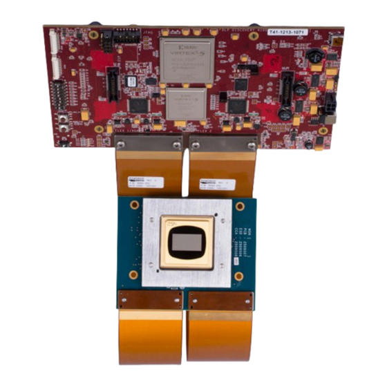
2.2 DLP Discovery 4100 Development Platform Photo...........................................................................................................
Components................................................................................................................................................................9
3 Hardware Overview and Setup............................................................................................................................................
3.1 Getting Started.................................................................................................................................................................
3.2 User Connectors and I/O.................................................................................................................................................
3.3 Configuration Jumpers.....................................................................................................................................................
3.4
Switches...........................................................................................................................................................................27
3.5 Power and Status LEDs...................................................................................................................................................
Points........................................................................................................................................................................30
4
Software.................................................................................................................................................................................31
4.1 Overview..........................................................................................................................................................................
4.3 Graphical User Interface..................................................................................................................................................
4.4 Script and Status Operations...........................................................................................................................................
4.5 DLPC410 Control Window...............................................................................................................................................
4.6 Test Patterns Window......................................................................................................................................................
Box.........................................................................................................................................................................56
4.8
Links.................................................................................................................................................................................56
Documentation........................................................................................................................................................57
6
Appendix................................................................................................................................................................................58
6.1 Abbreviations and Acronyms...........................................................................................................................................
6.2 Notational Conventions....................................................................................................................................................
7 Revision History...................................................................................................................................................................
Figure 2-2. DLPLCRC410EVM connected to DLPLCR95EVM...................................................................................................
Figure 2-3. DLPLCRC410EVM Controller Board Key Components............................................................................................
Figure 3-1. DLPLCRC410EVM Controller Connectors (Top View)............................................................................................
Figure 3-2. DLPLCRC410EVM Controller Connectors (Bottom View)......................................................................................
Figure 3-3. DLPLCRC410EVM Controller Configuration Jumpers............................................................................................
DLPU040B - OCTOBER 2016 - REVISED MARCH 2023
Submit Document Feedback
Table of Contents
Platform...............................................................................................................6
Operation........................................................................................................................................33
List of Figures
Diagram...........................................................................................................................................6
Copyright © 2023 Texas Instruments Incorporated
ABSTRACT
DLP
Table of Contents
®
Discovery™ 4100 Development Platform
4
8
12
12
12
26
29
32
39
51
53
54
58
58
60
8
9
12
13
26
1
Advertisement
Table of Contents

Related Manuals for Texas Instruments DLP Discovery 4100


Summary of Contents for Texas Instruments DLP Discovery 4100
-
Page 1: Table Of Contents
® Discovery™ 4100 Development Platform ABSTRACT The DLP Discovery 4100 Development Platform, or D4100 Platform, is an evaluation platform to experiment and develop with the DLP650LNIR, DLP7000, DLP9500, DLP7000UV, DLP9500UV, DLPC410, DLPR410 and DLPA200 chips. This platform targets applications needing: •... - Page 2 Table 4-1. DMD Characteristics..............................Table 4-2. SW1 Dip Switch Assignments...........................55 Trademarks ActiveX ™ is a trademark of ACTIVE NETWORK, LLC. ® Discovery™ 4100 Development Platform DLPU040B – OCTOBER 2016 – REVISED MARCH 2023 Submit Document Feedback Copyright © 2023 Texas Instruments Incorporated...
- Page 3 Trademarks All trademarks are the property of their respective owners. ® DLPU040B – OCTOBER 2016 – REVISED MARCH 2023 Discovery™ 4100 Development Platform Submit Document Feedback Copyright © 2023 Texas Instruments Incorporated...
-
Page 4: Introduction
1.1 Welcome The DLP Discovery 4100 Development Platform is a great way to evaluate the fastest binary pattern and data rates the DLP chip portfolio offers. Designers get pixel accurate control of all DMD micromirrors with Global, Quad, Dual and Single Block Modes available for tailoring DMD micromirror pattern timing for continuous (lamp) or solid state (switched) illuminated applications. -
Page 5: Overview
Overview 2 Overview DLP Discovery 4100 is a group of six evaluation modules which, when paired together, create a highly flexible platform to learn, experiment and develop with DLP technology. At the heart of the platform is the DLPLCRC410EVM controller board. The DLPLCRC410EVM board includes the DLPC410, DLPR410, DLPA200, digital receiver, flash, power management circuits, and supporting digital logic. -
Page 6: The Dlp Discovery 4100 Development Platform
Overview www.ti.com 2.1 The DLP Discovery 4100 Development Platform The DLP Discovery 4100 Development Platform (D4100 Platform) typically refers to the combination of one DLPLCRC410EVM plus one DMD EVM. Together these include: • 1 ea. DLPLCRC410EVM Controller Board • 1 ea. DMD board with DMD and DMD mounting mechanics (Type-A DMDs only) •... - Page 7 – Mictor test connectors for logic analyzer connection. – JTAG headers for device programming. – GPIO connectors for general purpose digital I/O. ® DLPU040B – OCTOBER 2016 – REVISED MARCH 2023 Discovery™ 4100 Development Platform Submit Document Feedback Copyright © 2023 Texas Instruments Incorporated...
-
Page 8: Dlp Discovery 4100 Development Platform Photo
Overview www.ti.com 2.2 DLP Discovery 4100 Development Platform Photo When the DLPLCRC410EVM and the DLPLCR95EVM are assembled together, the combined D4100 Platform is as shown in Figure 2-2. Other DMD EVMs connect to the DLPLCRC410EVM in a similar fashion and look very similar, except the DLPLCRC410EVM only uses a single flex cable (Flex 1) for connection between the Controller Board and the DMD Board. -
Page 9: Key Components
The APPSFPGA is connected to a number of I/O connectors, interface controllers, and memory for use in prototyping a custom control solution prior to developing a custom board solution. 2.3.2 DLPC410 - Digital Controller for DLP Discovery 4100 Chipset The D4100 chipset includes the DLPC410 controller (configured Xilinx Virtex 5 LX30) which exposes a high- speed 2xLVDS data and control interface for DMD control. - Page 10 This delivers 1 A at 0.9 V as a DDR2 reference voltage supply. 2.3.12.4 REG. 1.0 V This delivers 3 A at 1.0 V as the Virtex 5 core supply. ® Discovery™ 4100 Development Platform DLPU040B – OCTOBER 2016 – REVISED MARCH 2023 Submit Document Feedback Copyright © 2023 Texas Instruments Incorporated...
- Page 11 This delivers 3 A at 3.3 V to supply the DMD and USB controller. 2.3.12.8 REG. 12 V This delivers the 0.5 A at 12 V to supply the DLPA200. ® DLPU040B – OCTOBER 2016 – REVISED MARCH 2023 Discovery™ 4100 Development Platform Submit Document Feedback Copyright © 2023 Texas Instruments Incorporated...
-
Page 12: Hardware Overview And Setup
Input Power Connectors DLPC410 Mictor Connector J13, J14 DMD Flex Connectors Figure 3-1. DLPLCRC410EVM Controller Connectors (Top View) ® Discovery™ 4100 Development Platform DLPU040B – OCTOBER 2016 – REVISED MARCH 2023 Submit Document Feedback Copyright © 2023 Texas Instruments Incorporated... -
Page 13: Figure 3-2. Dlplcrc410Evm Controller Connectors (Bottom View)
Pin Number Pin Name Description Ground Ground +5V_IN +5 VDC input, 30W maximum. +5V_IN +5 VDC input, 30W maximum. ® DLPU040B – OCTOBER 2016 – REVISED MARCH 2023 Discovery™ 4100 Development Platform Submit Document Feedback Copyright © 2023 Texas Instruments Incorporated... -
Page 14: Table 3-3. J1 Usb Pinout
2.5 V GPIO_A3 AG16 GPIO_A7 AF20 GPIO_A2 AG17 GPIO_A6 AF19 GPIO_A1 AH19 GPIO_A5 AG12 GPIO_A0 AG20 GPIO_A4 AH12 ® Discovery™ 4100 Development Platform DLPU040B – OCTOBER 2016 – REVISED MARCH 2023 Submit Document Feedback Copyright © 2023 Texas Instruments Incorporated... -
Page 15: Table 3-6. J8 Dlpc410 Mictor Connector
AF12 ECP2_M_TP24 ECP2_M_TP13 AE11 ECP2_M_TP23 ECP2_M_TP14 ECP2_M_TP22 ECP2_M_TP15 AF11 ECP2_M_TP21 ECP2_M_TP16 AB12 ECP2_M_TP20 ECP2_M_TP17 AA16 ECP2_M_TP19 ECP2_M_TP18 AD13 ® DLPU040B – OCTOBER 2016 – REVISED MARCH 2023 Discovery™ 4100 Development Platform Submit Document Feedback Copyright © 2023 Texas Instruments Incorporated... -
Page 16: Table 3-7. J9 Usb/Appsfpga Mictor Connector
USB_FD11/ USB_CTRL2/ TST_HDR_BY1_3 TST_HDR_BY3_3 USB_FD12/ USB_CTRL3/ TST_HDR_BY1_4 TST_HDR_BY3_4 USB_FD13/ USB_FPGA_RESET/ TST_HDR_BY1_5 TST_HDR_BY3_5 USB_FD14/ USB_INT5/ TST_HDR_BY1_6 TST_HDR_BY3_6 USB_FD15/ TST_HDR_BY1_7 ® Discovery™ 4100 Development Platform DLPU040B – OCTOBER 2016 – REVISED MARCH 2023 Submit Document Feedback Copyright © 2023 Texas Instruments Incorporated... - Page 17 DDC_DOUT_A0_DPP DDC_DOUT_A0_DPN SCPDI DMD_A_RESET DMDSPARE0 MBRST1_11 MBRST1_5 MBRST1_4 MBRST1_0 MBRST1_3 MBRST1_2 MBRST1_8 DDC_DOUT_B0_DPP DDC_DOUT_B0_DPN DDC_DOUT_B2_DPP DDC_DOUT_B2_DPN DDC_DOUT_B4_DPP DDC_DOUT_B4_DPN ® DLPU040B – OCTOBER 2016 – REVISED MARCH 2023 Discovery™ 4100 Development Platform Submit Document Feedback Copyright © 2023 Texas Instruments Incorporated...
-
Page 18: Table 3-8. J13 Dmd Flex Connector 1
Pin Name DDC_DOUT_B6_DPP DDC_DOUT_B6_DPN DDC_SCTRL_B_DPP DDC_SCTRL_B_DPP DDC_DOUT_B8_DPP DDC_DOUT_B8_DPN DDC_DOUT_B10_DPP DDC_DOUT_B10_DPN DDC_DOUT_B12_DPP DDC_DOUT_B12_DPN DDC_DOUT_B14_DPP DDC_DOUT_B14_DPN 3.3 V 3.3 V ® Discovery™ 4100 Development Platform DLPU040B – OCTOBER 2016 – REVISED MARCH 2023 Submit Document Feedback Copyright © 2023 Texas Instruments Incorporated... - Page 19 DDC_DOUT_C0_DPP DDC_DOUT_C0_DPN SCPDI DMD_B_RESET DMDSPARE0 MBRST2_11 MBRST2_5 MBRST2_4 MBRST2_0 MBRST2_3 MBRST2_2 MBRST2_8 DDC_DOUT_D0_DPP DDC_DOUT_D0_DPN DDC_DOUT_D2_DPP DDC_DOUT_D2_DPN DDC_DOUT_D4_DPP DDC_DOUT_D4_DPN ® DLPU040B – OCTOBER 2016 – REVISED MARCH 2023 Discovery™ 4100 Development Platform Submit Document Feedback Copyright © 2023 Texas Instruments Incorporated...
-
Page 20: Table 3-9. J14 Dmd Flex Connector 2
Pin Name DDC_DOUT_D6_DPP DDC_DOUT_D6_DPN DDC_SCTRL_D_DPP DDC_SCTRL_D_DPP DDC_DOUT_D8_DPP DDC_DOUT_D8_DPN DDC_DOUT_D10_DPP DDC_DOUT_D10_DPN DDC_DOUT_D12_DPP DDC_DOUT_D12_DPN DDC_DOUT_D14_DPP DDC_DOUT_D14_DPN 3.3 V 3.3 V ® Discovery™ 4100 Development Platform DLPU040B – OCTOBER 2016 – REVISED MARCH 2023 Submit Document Feedback Copyright © 2023 Texas Instruments Incorporated... -
Page 21: Table 3-10. J15 Ddr2 Sodimm Connector
DDR2_D44 DDR2_D41 DDR2_DQS5_N DDR2_DM5 DDR2_DQS5_P DDR2_D42 DDR2_D46 DDR2_D43 DDR2_D47 DDR2_D48 DDR2_D52 DDR2_D49 DDR2_D53 DDR2_CK1_P DDR2_CK1_N DDR2_DQ56_N DDR2_DQ56_P DDR2_DM6 ® DLPU040B – OCTOBER 2016 – REVISED MARCH 2023 Discovery™ 4100 Development Platform Submit Document Feedback Copyright © 2023 Texas Instruments Incorporated... -
Page 22: Table 3-11. J16 Exp-1
AC32 EXP1_DIFF_21_N EXP1_DIFF_20 AB32 EXP1_SE_IO_32 EXP1_DIFF_31_P EXP1_DIFF_18 AF34 EXP1_SE_IO_33 EXP1_DIFF_31_N EXP1_DIFF_18 AE34 EXP1_DIFF_19_P AG32 EXP1_DIFF_16 EXP1_DIFF_19_N AH32 EXP1_DIFF_16 ® Discovery™ 4100 Development Platform DLPU040B – OCTOBER 2016 – REVISED MARCH 2023 Submit Document Feedback Copyright © 2023 Texas Instruments Incorporated... -
Page 23: Table 3-12. J16 Exp-1 Power And Ground
126, 127, 128, 129, 130, 131, 132 85, 86, 91, 92, 97, 98, 103, 104, 109, 110, 115, 116 VCC_3P3V ® DLPU040B – OCTOBER 2016 – REVISED MARCH 2023 Discovery™ 4100 Development Platform Submit Document Feedback Copyright © 2023 Texas Instruments Incorporated... -
Page 24: Table 3-13. J17 Exp-2 Connector
EXP2_DIFF_9_P EXP2_DIFF_8_P EXP2_DIFF_9_N EXP2_DIFF_8_N EXP2_DIFF_7_P EXP2_DIFF_6_P EXP2_DIFF_7_N EXP2_DIFF_6_N EXP2_DIFF_5_P EXP2_DIFF_4_P EXP2_DIFF_5_N EXP2_DIFF_4_N EXP2_DIFF_3_P EXP2_DIFF_2_P EXP2_DIFF_3_N EXP2_DIFF_2_N EXP2_DIFF_1_P EXP2_DIFF_0_P ® Discovery™ 4100 Development Platform DLPU040B – OCTOBER 2016 – REVISED MARCH 2023 Submit Document Feedback Copyright © 2023 Texas Instruments Incorporated... -
Page 25: Table 3-14. J17 Exp-2 Power And Ground
Table 3-15. H1 Xilinx APPSFPGA JTAG Header H1 Pin Number Pin Name 1, 3, 5, 7, 9, 11, 13 P2P5V 12, 14 ® DLPU040B – OCTOBER 2016 – REVISED MARCH 2023 Discovery™ 4100 Development Platform Submit Document Feedback Copyright © 2023 Texas Instruments Incorporated... -
Page 26: Configuration Jumpers
PROM to the APPSFPGA. Table 3-17. APPSFPGA Revision Select Jumper Position Revision Version ® Discovery™ 4100 Development Platform DLPU040B – OCTOBER 2016 – REVISED MARCH 2023 Submit Document Feedback Copyright © 2023 Texas Instruments Incorporated... -
Page 27: Switches
This section defines the function of the switches on the DLPLCRC410EVM Controller Board. Switches 1 through 4 locations are shown in Figure 3-4 Figure 3-4. DLPLCRC410EVM On-Board Switches ® DLPU040B – OCTOBER 2016 – REVISED MARCH 2023 Discovery™ 4100 Development Platform Submit Document Feedback Copyright © 2023 Texas Instruments Incorporated... -
Page 28: Table 3-20. Sw1 Dip Switch Assignments
TI highly recommends to first Park the DMD micromirrors by pressing SW3. ® Discovery™ 4100 Development Platform DLPU040B – OCTOBER 2016 – REVISED MARCH 2023 Submit Document Feedback Copyright © 2023 Texas Instruments Incorporated... -
Page 29: Power And Status Leds
D11 – VLED0: The APPSFPGA application defines this logic. Drive low to turn on the LED. Drive high to turn off the LED. ® DLPU040B – OCTOBER 2016 – REVISED MARCH 2023 Discovery™ 4100 Development Platform Submit Document Feedback Copyright © 2023 Texas Instruments Incorporated... -
Page 30: Test Points
TP24 GROUND TP25 VCC_1P8V TP26 POWER_STANDBY# TP27 DMDSPARE0 TP28 MBRST1_0 TP29 VCC_1P0V_DDC TP30 DMDSPARE0 TP31 SCPCLK TP32 VCC_1P0V ® Discovery™ 4100 Development Platform DLPU040B – OCTOBER 2016 – REVISED MARCH 2023 Submit Document Feedback Copyright © 2023 Texas Instruments Incorporated... -
Page 31: Software
This chapter describes the operation of the DLP Discovery 4100 Explorer Graphical User Interface (GUI) software. The Discovery 4100 Explorer GUI provides control and display functions for the DLP Discovery 4100 Development Platform via the USB 2.0 interface to the DLPLCRC410EVM. -
Page 32: Overview
Descriptions of the Discovery 4100 Explorer menus, toolbars and display windows • Operation instructions 4.1.1 Software Overview The DLP Discovery 4100 Explorer GUI allows the user to control the DLPLCRC410EVM controller board hardware via USB 2.0 (or 1.1). The software uses the Discovery 4100 ActiveX ™ control API which is documented separately in the DLP®... -
Page 33: Dlp Discovery 4100 Operation
3. Connect the DLP with a USB 2.0 [mini-B to Type A] cable and apply power to the DLP Discovery 4100 Development Platform. The operating system detects the USB device and automatically install or prompt to install the driver. -
Page 34: Figure 4-3. Browse For Driver Software
7. Click Let me pick from a list of device drivers on my computer. Figure 4-4. Pick from a list of Device Drivers ® Discovery™ 4100 Development Platform DLPU040B – OCTOBER 2016 – REVISED MARCH 2023 Submit Document Feedback Copyright © 2023 Texas Instruments Incorporated... -
Page 35: Figure 4-5. Select Universal Serial Bus Devices
8. Select Universal Serial Bus devices. Click Next. Figure 4-5. Select Universal Serial Bus devices 9. Click on Have Disk. Figure 4-6. Have Disk ® DLPU040B – OCTOBER 2016 – REVISED MARCH 2023 Discovery™ 4100 Development Platform Submit Document Feedback Copyright © 2023 Texas Instruments Incorporated... -
Page 36: Figure 4-7. Browse For .Inf File
11. Click TI D4100 Explorer 12. Click Next. Figure 4-8. Select TI D4100 Explorer 13. Windows installs the driver. ® Discovery™ 4100 Development Platform DLPU040B – OCTOBER 2016 – REVISED MARCH 2023 Submit Document Feedback Copyright © 2023 Texas Instruments Incorporated... -
Page 37: Figure 4-9. Driver Installation Window
15. Verify driver installation in Device Manager window as shown in Figure 4-10. Figure 4-10. Verify Device 16. Start the DLP Discovery Explorer GUI from the Start/Texas Instruments/DLP Discovery 4100 Explorer menu. ® DLPU040B – OCTOBER 2016 – REVISED MARCH 2023 Discovery™ 4100 Development Platform Submit Document Feedback Copyright ©... -
Page 38: Figure 4-11. Discovery 4100 Explorer Usb And Dmd - Connection Status
DMD. The answer is to always restart the GUI software program after connecting to a different Discovery EVM. ® Discovery™ 4100 Development Platform DLPU040B – OCTOBER 2016 – REVISED MARCH 2023 Submit Document Feedback Copyright © 2023 Texas Instruments Incorporated... -
Page 39: Graphical User Interface
The menu bar commands provide standard menu access to software commands as shown in Figure 4-13. Figure 4-13. Menu Bar ® DLPU040B – OCTOBER 2016 – REVISED MARCH 2023 Discovery™ 4100 Development Platform Submit Document Feedback Copyright © 2023 Texas Instruments Incorporated... -
Page 40: Figure 4-14. File Menu
4.3.1.3 DMD Menu The DMD menu is used to select the DLPC410 Control operation mode. Figure 4-16. DMD Menu ® Discovery™ 4100 Development Platform DLPU040B – OCTOBER 2016 – REVISED MARCH 2023 Submit Document Feedback Copyright © 2023 Texas Instruments Incorporated... -
Page 41: Figure 4-17. Execution Menu
• Set End – Sets the end point of command execution within the script. Figure 4-17. Execution Menu ® DLPU040B – OCTOBER 2016 – REVISED MARCH 2023 Discovery™ 4100 Development Platform Submit Document Feedback Copyright © 2023 Texas Instruments Incorporated... -
Page 42: Figure 4-18. Test Patterns Menu
The Help menu contains a link to standard Windows help file contents and the command to load the About dialog box. Figure 4-19. Help Menu ® Discovery™ 4100 Development Platform DLPU040B – OCTOBER 2016 – REVISED MARCH 2023 Submit Document Feedback Copyright © 2023 Texas Instruments Incorporated... -
Page 43: Figure 4-20. Toolbar
Set Start and Set End icons set the start point and end point of command execution within a script. 4.3.2.4 Help Button The Help button displays the help contents for the application. ® DLPU040B – OCTOBER 2016 – REVISED MARCH 2023 Discovery™ 4100 Development Platform Submit Document Feedback Copyright © 2023 Texas Instruments Incorporated... -
Page 44: Figure 4-21. Script Commands Window
Once you’ve selected the commands and options, click the Add button to add the command options to the script. Figure 4-21. Script Commands Window ® Discovery™ 4100 Development Platform DLPU040B – OCTOBER 2016 – REVISED MARCH 2023 Submit Document Feedback Copyright © 2023 Texas Instruments Incorporated... -
Page 45: Figure 4-22. Load Tab
Select the desired options and Add button to add the command to the script. Figure 4-22. Load Tab ® DLPU040B – OCTOBER 2016 – REVISED MARCH 2023 Discovery™ 4100 Development Platform Submit Document Feedback Copyright © 2023 Texas Instruments Incorporated... -
Page 46: Figure 4-23. Reset Tab
Multiple Blocks options. Select the option you want to use and click the Add button to add the command to the script. Figure 4-23. Reset Tab ® Discovery™ 4100 Development Platform DLPU040B – OCTOBER 2016 – REVISED MARCH 2023 Submit Document Feedback Copyright © 2023 Texas Instruments Incorporated... -
Page 47: Figure 4-24. Clear Tab
NOTE: The Global option is implemented in software by sequentially issuing a DMD Block Clear command to all the blocks on the DMD. Figure 4-24. Clear Tab ® DLPU040B – OCTOBER 2016 – REVISED MARCH 2023 Discovery™ 4100 Development Platform Submit Document Feedback Copyright © 2023 Texas Instruments Incorporated... -
Page 48: Figure 4-25. Float Tab
SW3 of the EVM, or an equivalent assertion of the PWR_FLOAT input pin of the DLPC410. Figure 4-25. Float Tab ® Discovery™ 4100 Development Platform DLPU040B – OCTOBER 2016 – REVISED MARCH 2023 Submit Document Feedback Copyright © 2023 Texas Instruments Incorporated... -
Page 49: Figure 4-26. Control Tab
NOTE: For more information on GPIO outputs see the DLP® Discovery™ 4100 Development Platform API Programmer’s Guide (DLPU039 § 5.2.24 and § 6.2.24). Figure 4-26. Control Tab ® DLPU040B – OCTOBER 2016 – REVISED MARCH 2023 Discovery™ 4100 Development Platform Submit Document Feedback Copyright © 2023 Texas Instruments Incorporated... -
Page 50: Figure 4-27. Status Window
4.3.4 Status Window The Status Windows displays the execution status, retrieved information and any responses sent back to the host from the DLP Discovery 4100 Development Platform after a command has been executed. Figure 4-27. Status Window 4.3.5 Script Window... -
Page 51: Script And Status Operations
3. Click the OK button and a message box appears to notify that the status log has been saved. Note Status files are saved with a .sts extension. ® DLPU040B – OCTOBER 2016 – REVISED MARCH 2023 Discovery™ 4100 Development Platform Submit Document Feedback Copyright © 2023 Texas Instruments Incorporated... - Page 52 Once the selection is made, you are first prompted to save the current status log and then a blank status is inserted. ® Discovery™ 4100 Development Platform DLPU040B – OCTOBER 2016 – REVISED MARCH 2023 Submit Document Feedback Copyright © 2023 Texas Instruments Incorporated...
-
Page 53: Dlpc410 Control Window
Refer to the DLPC410 data sheet (DLPS024) for detailed information on the DLPC410 input signals. Refer to the DLP Discovery 4100 Development Platform API Programmer’s Guide (DLPU039) for detailed information about the ActiveX functions called by the buttons on this DMD/DLPC410 Control menu page. -
Page 54: Test Patterns Window
GPIO_A(4 - 6) enable/disable. The [GPIOA 4], [GPIOA 5], and [GPIOA 6] selections in the Test Patterns window map directly to the GPIO_A4, GPIO_A5, and GPIO_A6 outputs of the APPSFPGA, found on connector GPIO_A. ® Discovery™ 4100 Development Platform DLPU040B – OCTOBER 2016 – REVISED MARCH 2023 Submit Document Feedback Copyright © 2023 Texas Instruments Incorporated... -
Page 55: Table 4-2. Sw1 Dip Switch Assignments
ON = Row Address Mode ON = Watchdog Timer (WDT) Enable, disables other resets Refer to the DLP Discovery 4100 Development Platform API Programmer’s Guide (DLPU039) for detailed information about the ActiveX functions called by the buttons on this Test Patterns menu page. -
Page 56: About Box
Software www.ti.com 4.7 About Box The About Box provides version information about various software and hardware of the DLP Discovery 4100 Development Platform. Figure 4-31. About Box 4.8 Links For more information about Texas Instruments DLP Discovery 4100 Development Platform visit www.ti.com/tool/... -
Page 57: Related Documentation
• DLP650LNIR Board CCA - circuit card assembly • DLP650LNIR Board BOM - circuit card assembly DLP DIscovery 4100 Development Platform API Programmer's Guide www.cypress.com for the Cypress CY7C68013A USB Controller www.xilinx.com APPSFPGA development tools and information ® DLPU040B – OCTOBER 2016 – REVISED MARCH 2023 Discovery™... -
Page 58: Appendix
6.1 Abbreviations and Acronyms The following lists abbreviations and acronyms used in this manual. APPSFPGA Xilinx Virtex 5 FPGA on DLPLCRC410EVM for customer applications D4100 Platform DLP Discovery 4100 Development Platform Direct Current Double Data Rate Digital Micromirror Device Evaluation Board... - Page 59 ® DLPU040B – OCTOBER 2016 – REVISED MARCH 2023 Discovery™ 4100 Development Platform Submit Document Feedback Copyright © 2023 Texas Instruments Incorporated...
-
Page 60: Revision History
NOTE: Page numbers for previous revisions may differ from page numbers in the current version. Changes from Revision A (November 2018) to Revision B (March 2023) Page • Added steps on Windows Installer Error for DLP Discovery 4100 Explorer GUI ..........33 Changes from Revision * (October 2016) to Revision A (November 2018) Page •... - Page 61 TI products. TI’s provision of these resources does not expand or otherwise alter TI’s applicable warranties or warranty disclaimers for TI products. TI objects to and rejects any additional or different terms you may have proposed. IMPORTANT NOTICE Mailing Address: Texas Instruments, Post Office Box 655303, Dallas, Texas 75265 Copyright © 2023, Texas Instruments Incorporated...
Need help?
Do you have a question about the DLP Discovery 4100 and is the answer not in the manual?
Questions and answers