
Subscribe to Our Youtube Channel
Related Manuals for Cypress Semiconductor CYS25G0101DX-ATC


Summary of Contents for Cypress Semiconductor CYS25G0101DX-ATC
- Page 1 CYS25G0101DX-ATC Evaluation Board User’s Guide Cypress Semiconductor Corporation • 3901 North First Street • San Jose • CA 95134 • 408-943-2600 March 19, 2002 [+] Feedback...
-
Page 2: Table Of Contents
Figure 19. Parallel Input Block Schematic Diagram ... 27 Figure 20. Signals Block Schematic Diagram ... 28 Figure 21. Power Supply Block Schematic Diagram ... 29 Figure 22. Control Block Schematic Diagram ... 30 CYS25G0101DX-ATC Evaluation Board User’s Guide [+] Feedback... - Page 3 CYS25G0101DX-ATC Evaluation Board User’s Guide List of Figures (continued) Figure 23. Reference Clock Block Schematic Diagram ... 31 Figure 24. CYS25G0101DX Evaluation Board PCB Mechanical Drawing ... 33 Figure 25. CYS25G0101DX Evaluation Board PCB Top Layer Silk Screen ... 34 Figure 26.
-
Page 4: Introduction
J13, J14, J15, J16 and J4 are Differential CML input and output and power supply for the option- al optical module daughter card. Table 5 idescribes the optical module interface and Table 6 idescribes the LED. Figure 3 shows the jumper orientations of the CYS25G0101DX Evaluation Board. CYS25G0101DX-ATC Evaluation Board User’s Guide [+] Feedback... -
Page 5: Figure 1. The Block Diagram Of The Cys25G0101Dx
TXCLKI 15:0 Input Register FIFO (5byte) SHIFTER LOOPTIME LINELOOP LOOPA OUT± Figure 1. The Block Diagram of the CYS25G0101DX CYS25G0101DX-ATC Evaluation Board User’s Guide (155.52MHz) TXCLKO REFCLK TX PLL Recovered Bit-Clock Tx Bit-Clock Lock-to-Ref Lock-to-Data / Clock Control Logic PWRDN LOCKREF (155.52MHz) -
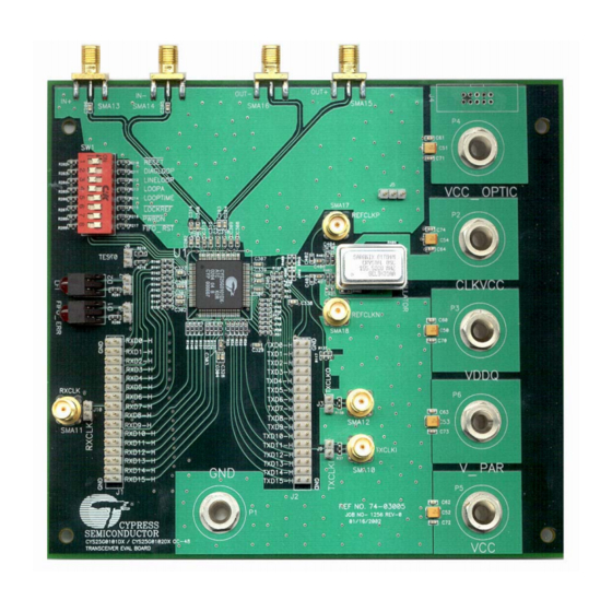
Page 6: Figure 2. The Cys25G0101Dx Evaluation Board
Header for CYS25G0101DX’s TXCLKO (pin 79) and GND. Figure 3 shows the orientation TxCLKO_H of this jumper Power supply for external optical module (see Table 5 for details) OPTIC POWER CYS25G0101DX-ATC Evaluation Board User’s Guide SMA16 SMA15 Description SMA17 SMA18... -
Page 7: Table 2. Pin Assignment Of J1 Header And Description Of J10 Header
Pin Number Name I/O Characteristics RXD15 HSTL output RXD14 HSTL output CYS25G0101DX-ATC Evaluation Board User’s Guide Description Description Parallel receive data output RXD15. The outputs change following RXCLK↓ Parallel receive data output RXD14. The outputs change following RXCLK↓ [+] Feedback... -
Page 8: Table 3. Pin Assignment Of J2 Header And Description Of J9 Header
TXD15 HSTL output TXD14 HSTL input TXD13 HSTL input CYS25G0101DX-ATC Evaluation Board User’s Guide Description Parallel receive data output RXD13. The outputs change following RXCLK↓ Parallel receive data output RXD12. The outputs change following RXCLK↓ Parallel receive data output RXD11. The outputs change following RXCLK↓... -
Page 9: Table 4. Functional Description Of Dip Switch 1 (Sw1)
DIAGLOOP 3, 4 LINELOOP, LOOPA OFF* CYS25G0101DX-ATC Evaluation Board User’s Guide Parallel transmit data input TXD12. The input data is sampled by TX- CLKI↑ Parallel transmit data input TXD10. The input data is sampled by TX- CLKI↑ Parallel transmit data input TXD9. The input data is sampled by TX- CLKI↑... -
Page 10: Table 5. Functional Description Of J4 Connector
1A, 1B, 3A, 3B VCC_OPTIC 2A, 2B, 4A, 4B Name FIFO_ERR CYS25G0101DX-ATC Evaluation Board User’s Guide State The transmission will be using the extracted receive bit-clock for the transmitted bit clock OFF* The transmission will be using the REFCLK input (155.52 MHz), which... -
Page 11: Figure 3. The Jumper Orientations Of The Cys25G0101Dx
FIFO_ERR RXCLK Pin 1 Figure 3. The Jumper Orientations of the CYS25G0101DX CYS25G0101DX-ATC Evaluation Board User’s Guide TXCLKO TXCLKI Pin 1 [+] Feedback... -
Page 12: Diagnostic Modes
Input Register FIFO (5byte) SHIFTER LINELOOP SW1-3 = OFF LOOPA SW1-4 = OFF OUT± Figure 4. Diagnostic Loopback Mode Data Path CYS25G0101DX-ATC Evaluation Board User’s Guide REFCLK RXCLKOUT TX PLL RX CDR 15:0 Output Register SHIFTER DIAGLOOP (SW1-2) = ON IN±... -
Page 13: Line Loopback
15:0 Input Register FIFO (5byte) SHIFTER LINELOOP SW1-3 = ON LOOPA SW1-4 = OFF OUT± CYS25G0101DX-ATC Evaluation Board User’s Guide REFCLK TX PLL Figure 5. Line Loopback Mode Data Path RXCLKOUT 15:0 Output Register SHIFTER RX CDR DIAGLOOP (SW1-2) = OFF IN±... -
Page 14: Analog Line Loopback
Register FIFO (5byte) SHIFTER LINELOOP SW1-3 = OFF LOOPA SW1-4 = ON OUT± Figure 6. Analog Line Loopback Mode Data Path CYS25G0101DX-ATC Evaluation Board User’s Guide REFCLK RXCLKOUT TX PLL RX CDR 15:0 Output Register SHIFTER DIAGLOOP (SW1-2) = OFF IN±... -
Page 15: Parallel Line Loopback" (Test0) Mode
SW1-3 = OFF SW1-3 = OFF LOOPA LOOPA SW1-4 = OFF SW1-4 = OFF OUT± OUT± Figure 7. Parallel Loopback (TEST0) Mode Data Path CYS25G0101DX-ATC Evaluation Board User’s Guide REFCLK REFCLK RXCLKOUT RXCLKOUT TX PLL TX PLL RX CDR RX CDR... -
Page 16: Testing Hookup
4. Power Supply – HP E3631A DC Power Supply * All equipment in the list is for reference only CLK2 Cypress CYS25G0101DX Evaluation Board CYS25G0101DX-ATC Evaluation Board User’s Guide Tektronix D3286 Pattern Analyzer Tektronix D3186 Pattern Generator 50 Ω Terminator... -
Page 17: Set-Up For Eye Diagram Test
* All equipment in the list is for reference only Tektronix D3186 Pattern Generator Trigger Out Cypress CYS25G0101DX Evaluation Board Figure 9. Equipment Set-up For Eye Diagram Test CYS25G0101DX-ATC Evaluation Board User’s Guide Agilent Infinium DAC 86100A Oscilloscope with 8348A Dual-Channel 50GHz Module OUT+ OUT- Trigger... -
Page 18: Sonet Jitter Transfer And Jitter Tolerance Test
* All equipment in the list is for reference only HP OmniBER 718 Communications Performance Analyzer Cypress CYS25G0101DX Evaluation Board Figure 10. Equipment Set-up For Jitter Test CYS25G0101DX-ATC Evaluation Board User’s Guide Optical to Analog Converter (i.e. HP’s 83446A) Analog to Optical Converter (i.e. HP’s 83430A) HP E3631A... -
Page 19: Set-Up For Testing The Tx Pll In Parallel Line Loopback Mode
C401 on C403 positions Cypress CYS25G0101DX Evaluation Board Figure 11. Equipment Set-up For Testing the TX PLL in Parallel Line Loopback Mode CYS25G0101DX-ATC Evaluation Board User’s Guide Tektronix D3286 Pattern Analyzer HP 8133A Pulse Generator (configure to Output = Input Clock divided by 16) -
Page 20: Eye Diagram Testing Result
CYS25G0101DX-ATC Evaluation Board User’s Guide 7. Eye Diagram Testing Result Figure 12 is the Eye Diagram measurement from CYS25G0101DX Evaluation Board by using the test set-up as in Figure 9. In this measurement, the evaluation board is configured to parallel loop back mode (Figure 7) and with no SONET filter at the oscilloscope. -
Page 21: Jitter Transfer Testing Result
CYS25G0101DX-ATC Evaluation Board User’s Guide 8. Jitter Transfer Testing Result Figure 13 and Figure 14 show the Jitter Transfer measurement by using the test set-up as in Figure 10. Figure 13 is the measurement result of the GR-253 (Bellcore) standard and Figure 14 is the measurement result of the G958 (ITU) standard. In this measurement, the CYS25G0101DX evaluation board is configured to parallel loopback mode (Figure 7). -
Page 22: Jitter Tolerance Testing Result
CYS25G0101DX-ATC Evaluation Board User’s Guide 9. Jitter Tolerance Testing Result Figure 15 and Figure 16 show the Jitter Tolerance measurement by using the test set-up as in Figure 10. Figure 15 is the measurement result of the GR-253 (Bellcore) standard and Figure 16 is the measurement result of the G825 (ITU) standard. In this measurement, the CYS25G0101DX evaluation board is configured to parallel loopback mode (Figure 7). -
Page 23: Schematic Diagram, Pcb Layout And Bom (Bill Of Material)
2. The operation current drawn by supply VCC at room temperature. 3. Assumes onboard clock option. If external clock (SMA option) is used the current drawn will depend on the termination resistors required for the external clock. CYS25G0101DX-ATC Evaluation Board User’s Guide Min. Max. -
Page 24: Appendix A: Schematic Diagrams Of The Cys25G0101Dx Evaluation Board
CYS25G0101DX-ATC Evaluation Board User’s Guide Appendix A: Schematic Diagrams of the CYS25G0101DX Evaluation Board [+] Feedback... -
Page 25: Figure 17. Top Level Of Cys25G0101Dx Evaluation Board Schematic Diagram
CYS25G0101DX-ATC Evaluation Board User’s Guide Figure 17. Top Level of CYS25G0101DX Evaluation Board Schematic Diagram [+] Feedback... -
Page 26: Figure 18. Parallel Output Block Schematic Diagram
CYS25G0101DX-ATC Evaluation Board User’s Guide Figure 18. Parallel Output Block Schematic Diagram [+] Feedback... -
Page 27: Figure 19. Parallel Input Block Schematic Diagram
CYS25G0101DX-ATC Evaluation Board User’s Guide Figure 19. Parallel Input Block Schematic Diagram [+] Feedback... -
Page 28: Figure 20. Signals Block Schematic Diagram
CYS25G0101DX-ATC Evaluation Board User’s Guide Figure 20. Signals Block Schematic Diagram [+] Feedback... -
Page 29: Figure 21. Power Supply Block Schematic Diagram
CYS25G0101DX-ATC Evaluation Board User’s Guide Figure 21. Power Supply Block Schematic Diagram [+] Feedback... -
Page 30: Figure 22. Control Block Schematic Diagram
CYS25G0101DX-ATC Evaluation Board User’s Guide Figure 22. Control Block Schematic Diagram [+] Feedback... -
Page 31: Figure 23. Reference Clock Block Schematic Diagram
CYS25G0101DX-ATC Evaluation Board User’s Guide Figure 23. Reference Clock Block Schematic Diagram [+] Feedback... -
Page 32: Appendix B: Pcb Layout Diagrams Of The Cys25G0101Dx Evaluation Board
CYS25G0101DX-ATC Evaluation Board User’s Guide Appendix B: PCB Layout Diagrams of the CYS25G0101DX Evaluation Board [+] Feedback... -
Page 33: Figure 24. Cys25G0101Dx Evaluation Board Pcb Mechanical Drawing
CYS25G0101DX-ATC Evaluation Board User’s Guide Figure 24. CYS25G0101DX Evaluation Board PCB Mechanical Drawing [+] Feedback... -
Page 34: Figure 25. Cys25G0101Dx Evaluation Board Pcb Top Layer Silk Screen
CYS25G0101DX-ATC Evaluation Board User’s Guide Figure 25. CYS25G0101DX Evaluation Board PCB Top Layer Silk Screen [+] Feedback... -
Page 35: Figure 26. Cys25G0101Dx Evaluation Board Pcb Top Layer Layout
CYS25G0101DX-ATC Evaluation Board User’s Guide Figure 26. CYS25G0101DX Evaluation Board PCB Top Layer Layout [+] Feedback... -
Page 36: Figure 27. Cys25G0101Dx Evaluation Board Pcb Top Layer Solder Mask
CYS25G0101DX-ATC Evaluation Board User’s Guide Figure 27. CYS25G0101DX Evaluation Board PCB Top Layer Solder Mask [+] Feedback... -
Page 37: Figure 28. Cys25G0101Dx Evaluation Board Pcb Power Plane Layout
CYS25G0101DX-ATC Evaluation Board User’s Guide Figure 28. CYS25G0101DX Evaluation Board PCB Power Plane Layout [+] Feedback... -
Page 38: Figure 29. Cys25G0101Dx Evaluation Board Pcb Ground Plane Layout
CYS25G0101DX-ATC Evaluation Board User’s Guide Figure 29. CYS25G0101DX Evaluation Board PCB Ground Plane Layout [+] Feedback... -
Page 39: Figure 30. Cys25G0101Dx Evaluation Board Pcb Bottom Silk Screen
CYS25G0101DX-ATC Evaluation Board User’s Guide Figure 30. CYS25G0101DX Evaluation Board PCB Bottom Silk Screen [+] Feedback... -
Page 40: Figure 31. Cys25G0101Dx Evaluation Board Pcb Bottom Layer Layout
CYS25G0101DX-ATC Evaluation Board User’s Guide Figure 31. CYS25G0101DX Evaluation Board PCB Bottom Layer Layout [+] Feedback... -
Page 41: Figure 32. Cys25G0101Dx Evaluation Board Pcb Bottom Solder Mask
CYS25G0101DX-ATC Evaluation Board User’s Guide Figure 32. CYS25G0101DX Evaluation Board PCB Bottom Solder Mask [+] Feedback... -
Page 42: Appendix C: Cys25G0101Dx Evaluation Board Lvpecl Bom (Bill Of Material)
CYS25G0101DX-ATC Evaluation Board User’s Guide Appendix C: CYS25G0101DX Evaluation Board LVPECL BOM (Bill of Material) [+] Feedback... -
Page 43: Table 8. Cys25G0101Dx Evaluation Board Lvpecl Bom - Page 1 Of 4
CYS25G0101DX-ATC Evaluation Board User’s Guide Table 8. CYS25G0101DX Evaluation Board LVPECL BOM - Page 1 of 4 [+] Feedback... -
Page 44: Table 9. Cys25G0101Dx Evaluation Board Lvpecl Bom - Page 2 Of 4
CYS25G0101DX-ATC Evaluation Board User’s Guide Table 9. CYS25G0101DX Evaluation Board LVPECL BOM - Page 2 of 4 [+] Feedback... -
Page 45: Table 10. Cys25G0101Dx Evaluation Board Lvpecl Bom - Page 3 Of 4
CYS25G0101DX-ATC Evaluation Board User’s Guide Table 10. CYS25G0101DX Evaluation Board LVPECL BOM - Page 3 of 4 [+] Feedback... -
Page 46: Table 11. Cys25G0101Dx Evaluation Board Lvpecl Bom - Page 4 Of 4
CYS25G0101DX-ATC Evaluation Board User’s Guide Table 11. CYS25G0101DX Evaluation Board LVPECL BOM - Page 4 of 4 [+] Feedback... -
Page 47: Appendix D: Cys25G0101Dx Evaluation Board Hstl Bom (Bill Of Material)
CYS25G0101DX-ATC Evaluation Board User’s Guide Appendix D: CYS25G0101DX Evaluation Board HSTL BOM (Bill of Material) [+] Feedback... -
Page 48: Table 12. Cys25G0101Dx Evaluation Board Hstl Bom - Page 1 Of 4
CYS25G0101DX-ATC Evaluation Board User’s Guide Table 12. CYS25G0101DX Evaluation Board HSTL BOM - Page 1 of 4 [+] Feedback... -
Page 49: Table 13. Cys25G0101Dx Evaluation Board Hstl Bom - Page 2 Of 4
CYS25G0101DX-ATC Evaluation Board User’s Guide Table 13. CYS25G0101DX Evaluation Board HSTL BOM - Page 2 of 4 [+] Feedback... -
Page 50: Table 14. Cys25G0101Dx Evaluation Board Hstl Bom - Page 3 Of 4
CYS25G0101DX-ATC Evaluation Board User’s Guide Table 14. CYS25G0101DX Evaluation Board HSTL BOM - Page 3 of 4 [+] Feedback... -
Page 51: Table 15. Cys25G0101Dx Evaluation Board Hstl Bom - Page 4 Of 4
CYS25G0101DX-ATC Evaluation Board User’s Guide Table 15. CYS25G0101DX Evaluation Board HSTL BOM - Page 4 of 4 © Cypress Semiconductor Corporation, 2002. The information contained herein is subject to change without notice. Cypress Semiconductor Corporation assumes no responsibility for the use of any circuitry other than circuitry embodied in a Cypress Semiconductor product.
Need help?
Do you have a question about the CYS25G0101DX-ATC and is the answer not in the manual?
Questions and answers