Sign In
Upload
Manuals
Brands
Cypress Semiconductor Manuals
Motherboard
CYS25G0101DX-ATC
Cypress Semiconductor CYS25G0101DX-ATC Manuals
Manuals and User Guides for Cypress Semiconductor CYS25G0101DX-ATC. We have
1
Cypress Semiconductor CYS25G0101DX-ATC manual available for free PDF download: User Manual
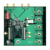
Cypress Semiconductor CYS25G0101DX-ATC User Manual (51 pages)
Cypress Evaluation Board User's Guide
Brand:
Cypress Semiconductor
| Category:
Motherboard
| Size: 2 MB
Table of Contents
Table of Contents
2
1 Introduction
4
2 Features
4
3 Kit Contents
4
4 Functional Description
4
Figure 1. the Block Diagram of the CYS25G0101DX
5
Figure 2. the CYS25G0101DX Evaluation Board
6
Table 2. Pin Assignment of J1 Header and Description of J10 Header
7
Table 3. Pin Assignment of J2 Header and Description of J9 Header
8
Table 4. Functional Description of DIP Switch 1 (SW1)
9
Table 5. Functional Description of J4 Connector
10
Table 6. Description of LED Indicators
10
Figure 3. the Jumper Orientations of the CYS25G0101DX
11
5 Diagnostic Modes
12
Diagnostic Loopback Mode
12
Figure 4. Diagnostic Loopback Mode Data Path
12
Line Loopback
13
Figure 5. Line Loopback Mode Data Path
13
Analog Line Loopback
14
Figure 6. Analog Line Loopback Mode Data Path
14
Parallel Line Loopback" (TEST0) Mode
15
Test the Internal RX CDR PLL Only
15
Test the Internal RX CDR PLL and TX PLL
15
Figure 7. Parallel Loopback (TEST0) Mode Data Path
15
6 Testing Hookup
16
Set-Up for BERT Test
16
Figure 8. Equipment Set-Up for BERT Test
16
Set-Up for Eye Diagram Test
17
Figure 9. Equipment Set-Up for Eye Diagram Test
17
SONET Jitter Transfer and Jitter Tolerance Test
18
Figure 10. Equipment Set-Up for Jitter Test
18
Set-Up for Testing the TX PLL in Parallel Line Loopback Mode
19
Figure 11. Equipment Set-Up for Testing the TX PLL in Parallel Line Loopback Mode
19
7 Eye Diagram Testing Result
20
Figure 12. CYS25G0101DX Evaluation Board Eye Diagram
20
8 Jitter Transfer Testing Result
21
Figure 13. CYS25G0101DX Evaluation Board GR-253 Jitter Transfer Testing Result
21
Figure 14. CYS25G0101DX Evaluation Board G958 Jitter Transfer Testing Result
21
9 Jitter Tolerance Testing Result
22
Figure 15. CYS25G0101DX Evaluation Board GR-253 Jittertolerance Testing Result
22
Figure 16. CYS25G0101DX Evaluation Board G825 Jitter Tolerance Testing Result
22
10 Schematic Diagram, PCB Layout and BOM (Bill of Material)
23
Table 7. Operation Specification of CYS25G0101DX Evaluation Board
23
Appendix A: Schematic Diagrams of the CYS25G0101DX Evaluation Board
24
Figure 17. Top Level of CYS25G0101DX Evaluation Board Schematic Diagram
25
Figure 18. Parallel Output Block Schematic Diagram
26
Figure 19. Parallel Input Block Schematic Diagram
27
Figure 20. Signals Block Schematic Diagram
28
Figure 21. Power Supply Block Schematic Diagram
29
Figure 22. Control Block Schematic Diagram
30
Figure 23. Reference Clock Block Schematic Diagram
31
Appendix B: PCB Layout Diagrams of the CYS25G0101DX Evaluation Board
32
Figure 24. CYS25G0101DX Evaluation Board PCB Mechanical Drawing
33
Figure 25. CYS25G0101DX Evaluation Board PCB Top Layer Silk Screen
34
Figure 26. CYS25G0101DX Evaluation Board PCB Top Layer Layout
35
Figure 27. CYS25G0101DX Evaluation Board PCB Top Layer Solder Mask
36
Figure 28. CYS25G0101DX Evaluation Board PCB Power Plane Layout
37
Figure 29. CYS25G0101DX Evaluation Board PCB Ground Plane Layout
38
Figure 30. CYS25G0101DX Evaluation Board PCB Bottom Silk Screen
39
Figure 31. CYS25G0101DX Evaluation Board PCB Bottom Layer Layout
40
Figure 32. CYS25G0101DX Evaluation Board PCB Bottom Solder Mask
41
Appendix C: CYS25G0101DX Evaluation
42
Table 8. CYS25G0101DX Evaluation Board LVPECL BOM - Page 1 of 4
43
Table 9. CYS25G0101DX Evaluation Board LVPECL BOM - Page 2 of 4
44
Table 10. CYS25G0101DX Evaluation Board LVPECL BOM - Page 3 of 4
45
Table 11. CYS25G0101DX Evaluation Board LVPECL BOM - Page 4 of 4
46
Appendix C: CYS25G0101DX Evaluation Board LVPECL BOM (Bill of Material)
42
Appendix D: CYS25G0101DX Evaluation Board HSTL BOM (Bill of Material)
47
Table 12. CYS25G0101DX Evaluation Board HSTL BOM - Page 1 of 4
48
Table 13. CYS25G0101DX Evaluation Board HSTL BOM - Page 2 of 4
49
Table 14. CYS25G0101DX Evaluation Board HSTL BOM - Page 3 of 4
50
Table 15. CYS25G0101DX Evaluation Board HSTL BOM - Page 4 of 4
51
Advertisement
Advertisement
Related Products
Cypress Semiconductor CYP15G0101DXB
Cypress Semiconductor CY8CKIT-037
Cypress Semiconductor CYALKIT-E04 Series
Cypress Semiconductor CYALKIT-E04 S6AE102A
Cypress Semiconductor CYALKIT-E04 S6AE103A
Cypress Semiconductor CY8CKIT-026
Cypress Semiconductor CYUSB3KIT-003
Cypress Semiconductor CapSense Express CY3218-CAPEXP2
Cypress Semiconductor CY8CKIT-028-TFT
Cypress Semiconductor CY8CKIT-028-EPD
Cypress Semiconductor Categories
Computer Hardware
Motherboard
Microcontrollers
Controller
Network Hardware
More Cypress Semiconductor Manuals
Login
Sign In
OR
Sign in with Facebook
Sign in with Google
Upload manual
Upload from disk
Upload from URL