
Related Manuals for Cypress Semiconductor CYP15G0101DXB


Summary of Contents for Cypress Semiconductor CYP15G0101DXB
- Page 1 CYP15G0101DXB Evaluation Board User’s Guide Cypress Semiconductor Corporation • 3901 North First Street • San Jose CA 95134 • 408-943-2600 August 12, 2003 [+] Feedback...
-
Page 2: Table Of Contents
7. Schematic Diagram, PCB Layout, and Bill of Materials (BOM) ..................23 Appendix A. Schematic Diagram of CYP15G0101DXB Evaluation Board ................24 Appendix B. PCB Layout for CYP15G0101DXB Evaluation Board ..................30 Appendix C. Bill Of Materials (BOM) CYP15G0101DXB Evaluation Board ................. 39 [+] Feedback... - Page 3 Figure 16. Adding Two Framing Characters to Data Stream ....................22 Figure 17. CYP15G0101DXB-EVAL Top Level Schematics ....................25 Figure 18. CYP15G0101DXB-EVAL Terminated Transmitter & Receiver Blocks ............... 26 Figure 19. CYP15G0101DXB-EVAL Terminated Control Signals Block ................27 Figure 20. CYP15G0101DXB-EVAL Transmit and Receive Clock Schematics ..............28 Figure 21.
- Page 4 CYP15G0101DXB Evaluation Board User’s Guide List of Tables Table 1. Description of Connectors of the CYP15G0101DXB Evaluation Board ............... 10 Table 2. Description of Control Pins in JT7 ........................... 11 Table 3. The High, Mid, and Low Levels on JT32 ........................15 Table 4.
-
Page 5: Overview
195 to 1500 MBaud. This document describes the operation and interface of the CYP15G0101DXB evaluation board. The evaluation board allows users to become familiar with the functionality of the CYP15G0101DXB. Figure 4 gives a skeletal view of the evaluation board. 2. Kit Contents •... -
Page 6: Functional Description Of Cyp15G0101Dxb
CYP15G0101DXB Evaluation Board User’s Guide 4. Functional Description of CYP15G0101DXB Figure 2 shows the block diagram of CYP15G0101DXB, which has a pair of transmit and receive channels. Figure 1 shows the transmitter section of CYP15G0101DXB. CHARACTER-RATE CLOCK TRANSMIT PLL BIT-RATE CLOCK... -
Page 7: Figure 3. Cyp15G0101Dxb Receiver Section Block Diagram
CYP15G0101DXB Evaluation Board User’s Guide Figure 3 shows the receive section of the CYP15G0101DXB. The serial data input passes through the framer (where the recovered bit stream is framed to framing character), the 10B/8B Decoder and the elasticity buffer. RX-PLL Enable... -
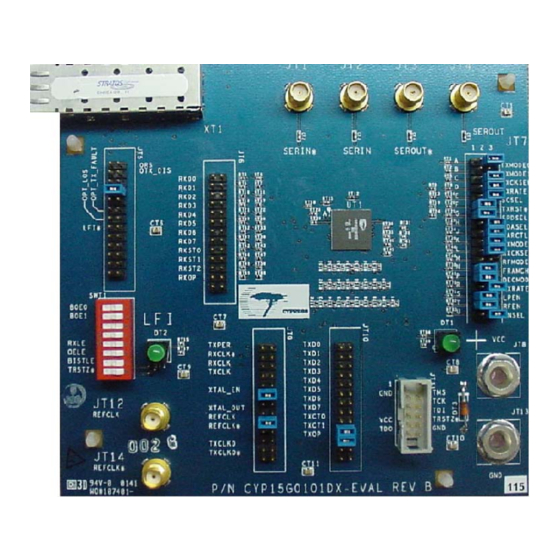
Page 8: Board Layout, Photograph And Pin Descriptions
CYP15G0101DXB Evaluation Board User’s Guide 5. Board Layout, Photograph and Pin Descriptions Figure 4 shows the skeletal view of the CYP15G0101DX board. Figure 4. CYP15G0101DXB-EVAL Skeletal View [+] Feedback... -
Page 9: Figure 5. Pin Description Of Cyp15G0101Dxb-Eval
CYP15G0101DXB Evaluation Board User’s Guide Figure 5 shows the different connectors and pins of the evaluation board for CYP15G0101DXB. Figure 5. Pin Description of CYP15G0101DXB-EVAL [+] Feedback... -
Page 10: Table 1. Description Of Connectors Of The Cyp15G0101Dxb Evaluation Board
Power On Indicator Indicates if the power supply is ON. The LED glows when the power supply goes JT11 JTAG Interface Note: For CYP15G0101DXB, there is no dedicated JTAG reset. The JTAG logic will be reset on power-on. JT10 TXD[7:0]... -
Page 11: Table 2. Description Of Control Pins In Jt7
CYP15G0101DXB Evaluation Board User’s Guide Table 1. Description of Connectors of the CYP15G0101DXB Evaluation Board (continued) Connectors Signals Description JT12 REFCLK External differential Reference clock. For single ended REFCLK input, apply an LVTTL clock signal to REFCLK input in JT12. - Page 12 — The elasticity buffer is bypassed. • H: Invalid State. RFMODE Reframe Mode Select. 3-Level Select Please refer to the data sheet for CYP15G0101DXB for detailed information. FRAMCHAR Framing Character Select. 3-Level select. Please refer to the data sheet for CYP15G0101DXB for detailed information.
-
Page 13: Test Modes
The different test modes discussed in this document are as follows: 1. BIST mode CYP15G0101DXB has the Built-In Self-Test (BIST) capability. The transmit and receive channel contain the BIST Pattern Generator and Checker respectively. Figure 6 shows the BIST mode operation. -
Page 14: Adjusting Settings On The Board
CYP15G0101DXB Evaluation Board User’s Guide 2. Parallel Data In and Parallel Data Out mode — Encoded Mode — Unencoded Mode The variations discussed in this document, for this mode are — Parallel-In – Serial-Out Mode. (testing the transmit side) — Different Clock Source (i.e., internal vs. external; different frequency mode, etc.) The detailed description will be comprised of —... -
Page 15: Bist Test Set-Up
CYP15G0101DXB Evaluation Board User’s Guide The 2-level dip switches on SWT1 are configured high or low as illustrated in Figure 9. Push this side to set HIGH Push this side to set LOW Figure 9. Controlling SWT1 Dip Switches Settings JT7 pins have 3-level inputs. -
Page 16: Test Equipment Set-Up
Figure 11. Pictorial Representation of the Internal BIST Set-up 6.2.1.3 Test Set-up The intention of this set-up is to test CYP15G0101DXB in BIST mode. Follow the procedure below for the test set-up. 1. Connect the clock input to the internal clock by placing a shunt across the XTAL_OUT on JT9. -
Page 17: Figure 12. Signal On Rxst1 When Bist Is Successful
CYP15G0101DXB Evaluation Board User’s Guide 8. Toggle TRSTZ* to LOW for a short moment and toggle to HIGH again, which will reset the board. 9. Push RXLE and OELE HIGH and BISTLE to LOW 10.Enable necessary transmit and receive channels by keeping the corresponding BOEs HIGH as shown in Table 5. To perform BIST, enable all channels. -
Page 18: Bist External Loopback Mode
CYP15G0101DXB Evaluation Board User’s Guide Figure 13. The Eye Diagram through the Signal Analyzer 6.2.2 BIST External Loopback Mode 6.2.2.1 Equipment Required Equipment needed is the same as mentioned in Section 6.2.1.1 on page 15. 6.2.2.2 Test Set-up Retain the initial set-up for the Internal BIST set-up as described in Section 6.2.1.3 and then follow the procedures below. -
Page 19: Parallel Data In - Parallel Data Out Mode
CYP15G0101DXB Evaluation Board User’s Guide 6.3 Parallel Data In – Parallel Data Out Mode The intention of this set-up is to test CYP15G0101DXB in parallel-in and parallel-out mode for encoded and unencoded data. 6.3.1 Encoded Mode 6.3.1.1 Equipment Required Equipment needed: •... -
Page 20: Result Verification
CYP15G0101DXB Evaluation Board User’s Guide Table 6. The Levels of Static Signals on JT32 for Parallel In-Parallel Out Mode (Encoded) Signal Level Signal Level Signal Level TXMODE0 SPDSEL HIGH FRAMCHAR HIGH TXMODE1 SDASEL DECMODE HIGH TXCKSEL PARCTL RXRATE TXRATE RXMODE... -
Page 21: Table 7. The Levels Of Static Signals On Jt32 For Parallel In-Parallel Out Mode (Unencoded)
CYP15G0101DXB Evaluation Board User’s Guide Table 7. The Levels of Static Signals on JT32 for Parallel In-Parallel Out Mode (Unencoded) Signal Level Signal Level Signal Level TXMODE0 SPDSEL HIGH FRAMCHAR HIGH TXMODE1 SDASEL DECMODE TXCKSEL PARCTL RXRATE TXRATE RXMODE LPEN... -
Page 22: Result Verification
CYP15G0101DXB Evaluation Board User’s Guide The DG2020 data pattern provided by Cypress does not contain any framing patterns for the unencoded mode. In order for HOTLink to frame the data properly, two consecutive K28.5’s need to be added to the DG2020 pattern. -
Page 23: Schematic Diagram, Pcb Layout, And Bill Of Materials (Bom)
Figure 17 to Figure 21 in Appendix A shows the schematic diagram of the CYP15G0101DXB-EVAL. Figure 22 to Figure 29 in Appendix B shows the PCB layout of each layer of the CYP15G0101DXB-EVAL. The Bill of Materials (BOM) of the evaluation board is listed in Appendix C in Table 11. -
Page 24: Appendix A. Schematic Diagram Of Cyp15G0101Dxb Evaluation Board
CYP15G0101DXB Evaluation Board User’s Guide Appendix A. Schematic Diagram of CYP15G0101DXB Evaluation Board [+] Feedback... -
Page 25: Figure 17. Cyp15G0101Dxb-Eval Top Level Schematics
CYP15G0101DXB Evaluation Board User’s Guide Figure 17. CYP15G0101DXB-EVAL Top Level Schematics [+] Feedback... -
Page 26: Figure 18. Cyp15G0101Dxb-Eval Terminated Transmitter & Receiver Blocks
CYP15G0101DXB Evaluation Board User’s Guide Figure 18. CYP15G0101DXB-EVAL Terminated Transmitter & Receiver Blocks [+] Feedback... -
Page 27: Figure 19. Cyp15G0101Dxb-Eval Terminated Control Signals Block
CYP15G0101DXB Evaluation Board User’s Guide Figure 19. CYP15G0101DXB-EVAL Terminated Control Signals Block [+] Feedback... -
Page 28: Figure 20. Cyp15G0101Dxb-Eval Transmit And Receive Clock Schematics
CYP15G0101DXB Evaluation Board User’s Guide Figure 20. CYP15G0101DXB-EVAL Transmit and Receive Clock Schematics [+] Feedback... -
Page 29: Figure 21. Cyp15G0101Dxb-Eval Input Power Schematics
CYP15G0101DXB Evaluation Board User’s Guide Figure 21. CYP15G0101DXB-EVAL Input Power Schematics [+] Feedback... -
Page 30: Appendix B. Pcb Layout For Cyp15G0101Dxb Evaluation Board
CYP15G0101DXB Evaluation Board User’s Guide Appendix B. PCB Layout for CYP15G0101DXB Evaluation Board [+] Feedback... -
Page 31: Figure 22. Cyp15G0101Dxb-Eval Top Layout
CYP15G0101DXB Evaluation Board User’s Guide Figure 22. CYP15G0101DXB-EVAL Top Layout [+] Feedback... -
Page 32: Figure 23. Cyp15G0101Dxb-Eval Bottom Layout
CYP15G0101DXB Evaluation Board User’s Guide Figure 23. CYP15G0101DXB-EVAL Bottom Layout [+] Feedback... -
Page 33: Figure 24. Cyp15G0101Dxb-Eval Top Layer Silk Layout
CYP15G0101DXB Evaluation Board User’s Guide Figure 24. CYP15G0101DXB-EVAL Top Layer Silk Layout [+] Feedback... -
Page 34: Figure 25. Cyp15G0101Dxb-Eval Bottom Layer Silk Layout
CYP15G0101DXB Evaluation Board User’s Guide Figure 25. CYP15G0101DXB-EVAL Bottom Layer Silk Layout [+] Feedback... -
Page 35: Figure 26. Cyp15G0101Dxb-Eval Top Layer Solder Mask Layout
CYP15G0101DXB Evaluation Board User’s Guide Figure 26. CYP15G0101DXB-EVAL Top Layer Solder Mask Layout [+] Feedback... -
Page 36: Figure 27. Cyp15G0101Dxb-Eval Bottom Layer Solder Mask Layout
CYP15G0101DXB Evaluation Board User’s Guide Figure 27. CYP15G0101DXB-EVAL Bottom Layer Solder Mask Layout [+] Feedback... -
Page 37: Figure 28. Cyp15G0101Dxb-Eval Power Plane Layout
CYP15G0101DXB Evaluation Board User’s Guide Figure 28. CYP15G0101DXB-EVAL Power Plane Layout [+] Feedback... -
Page 38: Figure 29. Cyp15G0101Dxb-Eval Ground Plane Layout
CYP15G0101DXB Evaluation Board User’s Guide Figure 29. CYP15G0101DXB-EVAL Ground Plane Layout [+] Feedback... -
Page 39: Appendix C. Bill Of Materials (Bom) Cyp15G0101Dxb Evaluation Board
CYP15G0101DXB Evaluation Board User’s Guide Appendix C. Bill Of Materials (BOM) CYP15G0101DXB Evaluation Board [+] Feedback... -
Page 40: Table 11.Cyp15G0101Dxb Eval Board Bill Of Materials
CYP15G0101DXB Evaluation Board User’s Guide Table 11.CYP15G0101DXB Eval Board Bill Of Materials Part Name Ref Des Manufacturer MAN_PN CAP-.1UF CB1,CB2,CB5, Vishay VJ0805Y104KXJAT CB6,CB7,CB8, CB9,CT1,CT6, CT7,CT8,CT9, CT10,CT11 CAP-SMDC0805V-2400PF CT2,CT3,CT4, CT5 DIELECTRIC LABORATO- C08BLBB1X5UX RIES CAPPOL-10UF CB3,CB4,CB10 VISHAY 293D106X9010C2T CLK_HCMOS-LCC197X295P4 Connor Winfield HSM923-125.00MHZ... - Page 41 © Cypress Semiconductor Corporation, 2001. The information contained herein is subject to change without notice. Cypress Semiconductor Corporation assumes no responsibility for the use of any circuitry other than circuitry embodied in a Cypress Semiconductor product. Nor does it convey or imply any license under patent or other rights. Cypress Semiconductor does not authorize its products for use as critical components in life-support systems where a malfunction or failure may reasonably be expected to result in significant injury to the user.
Need help?
Do you have a question about the CYP15G0101DXB and is the answer not in the manual?
Questions and answers