Table of Contents
Advertisement
Quick Links
Features
■
Fully registered inputs and outputs for pipelined operation
■
128K x 36 common IO architecture
■
3.3V core power supply (V
DD
■
2.5V/3.3V IO power supply (V
■
Fast clock to output times: 2.6 ns (for 250 MHz device)
■
User-selectable burst counter supporting Intel
interleaved or linear burst sequences
■
Separate processor and controller address strobes
■
Synchronous self-timed writes
■
Asynchronous output enable
■
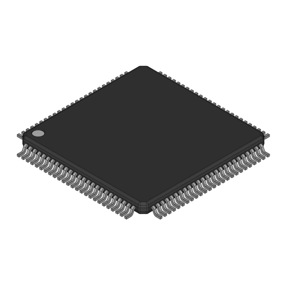
Offered in Pb-free 100-Pin TQFP, Pb-free and non Pb-free
119-Ball BGA package, and 165-Ball FBGA package
■
"ZZ" sleep mode option and stop clock option
■
Available in industrial and commercial temperature ranges
Selection Guide
Specification
Maximum Access Time
Maximum Operating Current
Maximum CMOS Standby Current
Note
1. For best practice recommendations, refer to the Cypress application note
Cypress Semiconductor Corporation
Document #: 38-05516 Rev. *F
4-Mbit (128K x 36) Pipelined Sync SRAM
)
)
DDQ
®
®
Pentium
250 MHz
200 MHz
2.6
2.8
325
265
40
40
•
198 Champion Court
Functional Description
The CY7C1347G is a 3.3V, 128K x 36 synchronous-pipelined
SRAM designed to support zero-wait-state secondary cache
with minimal glue logic. CY7C1347G IO pins can operate at
either the 2.5V or the 3.3V level. The IO pins are 3.3V tolerant
when V
= 2.5V. All synchronous inputs pass through input
DDQ
registers controlled by the rising edge of the clock. All data
outputs pass through output registers controlled by the rising
edge of the clock. Maximum access delay from the clock rise is
2.6 ns (250 MHz device). CY7C1347G supports either the
interleaved burst sequence used by the Intel Pentium processor
or a linear burst sequence used by processors such as the
®
PowerPC
. The burst sequence is selected through the MODE
pin. Accesses can be initiated by asserting either the Address
Strobe from Processor (ADSP) or the Address Strobe from
Controller (ADSC) at clock rise. Address advancement through
the burst sequence is controlled by the ADV input. A 2-bit on-chip
wraparound burst counter captures the first address in a burst
sequence and automatically increments the address for the rest
of the burst access.
Byte write operations are qualified with the four Byte Write Select
(BW
) inputs. A Global Write Enable (GW) overrides all byte
[A:D]
write inputs and writes data to all four bytes. All writes are
conducted with on-chip synchronous self-timed write circuitry.
Three synchronous Chip Selects (CE
asynchronous Output Enable (OE) provide for easy bank
selection and output tri-state control. To provide proper data
during depth expansion, OE is masked during the first clock of a
read cycle when emerging from a deselected state.
166 MHz
3.5
240
40
AN1064, SRAM System
Guidelines.
,
•
San Jose
CY7C1347G
[1]
, CE
, CE
1
2
133 MHz
Unit
4.0
ns
225
mA
40
mA
CA 95134-1709
•
408-943-2600
Revised January 15, 2009
) and an
3
[+] Feedback
Advertisement
Table of Contents

Related Manuals for Cypress Semiconductor CY7C1347G


Summary of Contents for Cypress Semiconductor CY7C1347G
- Page 1 The CY7C1347G is a 3.3V, 128K x 36 synchronous-pipelined SRAM designed to support zero-wait-state secondary cache with minimal glue logic. CY7C1347G IO pins can operate at either the 2.5V or the 3.3V level. The IO pins are 3.3V tolerant when V = 2.5V.
-
Page 2: Block Diagram
[1:0] BURST COUNTER LOGIC ,DQP BYTE WRITE DRIVER D QP BYTE WRITE DRIVER MEMORY ARRAY D QP BYTE WRITE DRIVER BYTE WRITE DRIVER PIPELINED ENABLE CY7C1347G OUTPUT OUTPUT SENSE BUFFERS REGISTERS AMPS INPUT REGISTERS Page 2 of 22 [+] Feedback... - Page 3 Pinouts BYTE C BYTE D Document #: 38-05516 Rev. *F Figure 1. 100-Pin TQFP CY7C1347G CY7C1347G BYTE B BYTE A Page 3 of 22 [+] Feedback...
- Page 4 NC/288M NC/144M NC/288M NC/144M NC/72M MODE NC/36M Document #: 38-05516 Rev. *F Figure 2. 119-Ball BGA ADSP ADSC MODE NC/72M Figure 3. 165-Ball FBGA NC/18M CY7C1347G NC/576M NC/1G NC/36M ADSC NC/576M ADSP NC/1G NC/9M Page 4 of 22 [+] Feedback...
- Page 5 CE is sampled only when a new external address is loaded. is deasserted HIGH. CY7C1347G , CE , and CE are sampled active. A...
-
Page 6: Functional Overview
A synchronous self-timed write mechanism is provided to simplify the write operations. Because the CY7C1347G is a common IO device, the Output Enable (OE) must be deasserted HIGH before presenting data to the DQs and DQPs inputs. Doing so tri-states the output drivers. - Page 7 This parameter is sampled ADSP ADSC ADV WRITE , BW , BW , BW ) and BWE = L or GW = L. WRITE = H when all Byte Write Enable signals (BW CY7C1347G Second Third Fourth Address Address Address...
- Page 8 7. This table is only a partial listing of the byte write combinations. Any combination of BW Document #: 38-05516 Rev. *F ADSP ADSC ADV WRITE [2, 7] is valid. Appropriate write is based on which byte write is active. CY7C1347G L-H D L-H D L-H Q L-H Tri-State...
-
Page 9: Maximum Ratings
< 0.3V or V > V – 0.3V, /2). Undershoot: V (AC) > –2V (pulse width less than t (min) within 200 ms. During this time V < V and V CY7C1347G Ambient Temperature 2.5V −5% 0°C to +70°C 3.3V −5%/+10% to V –40°C to +85°C... -
Page 10: Thermal Resistance
R = 351Ω INCLUDING JIG AND SCOPE R = 1667Ω 2.5V OUTPUT 5 pF R = 1538Ω INCLUDING JIG AND SCOPE CY7C1347G 119 BGA 165 FBGA 119 BGA 165 FBGA Package Package 34.1 20.3 14.0 ALL INPUT PULSES ≤ 1 ns ≤... -
Page 11: Switching Characteristics
SRAMs when sharing the same data bus. OELZ = 2.5V on all data sheets. on page 10 unless otherwise noted. CY7C1347G –166 –133 (min) initially before a read or write operation can be initiated. on page 10. Transition is measured ±200 mV... -
Page 12: Switching Waveforms
Q(A2 + 1) Q(A2 + 2) Q(A1) BURST READ DON’T CARE UNDEFINED is HIGH, and CE is LOW. When CE is HIGH, CE CY7C1347G Burst continued with new base address Deselect cycle t CHZ Q(A2 + 3) Q(A2) Q(A2 + 1) - Page 13 WEH ADV suspends burst D(A2) D(A2 + 1) D(A2 + 1) D(A2 + 2) BURST WRITE DON’T CARE UNDEFINED LOW. CY7C1347G t ADS t ADH t WES t WEH ADVH ADVS D(A2 + 3) D(A3) D(A3 + 1) D(A3 + 2)
- Page 14 Figure 7. Read/Write Cycle Timing t WES t WEH t DS t DH t OELZ D(A3) t OEHZ Q(A4) Single WRITE DON’T CARE UNDEFINED CY7C1347G D(A5) D(A6) Q(A4+1) Q(A4+2) Q(A4+3) BURST READ Back-to-Back WRITEs Page 14 of 22 [+] Feedback...
- Page 15 Document #: 38-05516 Rev. *F [20, 21] Figure 8. ZZ Mode Timing DESELECT or READ Only High-Z DON’T CARE Table 5 on page 7 for all possible signal conditions to deselect the device. CY7C1347G t ZZREC t RZZI Page 15 of 22 [+] Feedback...
-
Page 16: Ordering Information
Table 7. Ordering Information Speed Package Ordering Code (MHz) Diagram CY7C1347G-133AXC 51-85050 100-Pin Thin Quad Flat Pack (14 x 20 x 1.4 mm) Pb-Free CY7C1347G-133BGC 51-85115 119-Ball Ball Grid Array (14 x 22 x 2.4 mm) CY7C1347G-133BGXC CY7C1347G-133BZC 51-85180 165-Ball Fine-Pitch Ball Grid Array (13 x 15 x 1.4 mm) - Page 17 Table 7. Ordering Information (continued) Speed Package Ordering Code (MHz) Diagram CY7C1347G-250AXC 51-85050 100-Pin Thin Quad Flat Pack (14 x 20 x 1.4 mm) Pb-Free CY7C1347G-250BGC 51-85115 119-Ball Ball Grid Array (14 x 22 x 2.4 mm) CY7C1347G-250BGXC CY7C1347G-250BZC 51-85180 165-Ball Fine-Pitch Ball Grid Array (13 x 15 x 1.4 mm)
-
Page 18: Package Diagrams
2. BODY LENGTH DIMENSION DOES NOT INCLUDE MOLD PROTRUSION/END FLASH MOLD PROTRUSION/END FLASH SHALL NOT EXCEED 0.0098 in (0.25 mm) PER SIDE BODY LENGTH DIMENSIONS ARE MAX PLASTIC BODY SIZE INCLUDING MOLD MISMATCH 3. DIMENSIONS IN MILLIMETERS CY7C1347G 1.40±0.05 12°±1° SEE DETAIL (8X) 0.20 MAX. - Page 19 CY7C1347G Package Diagrams (continued) Figure 10. 119-Ball BGA (14 x 22 x 2.4 mm), 51-85115 51-85115 *B Document #: 38-05516 Rev. *F Page 19 of 22 [+] Feedback...
- Page 20 Figure 11. 165-Ball FBGA (13 x 15 x 1.4 mm), 51-85180 TOP VIEW PIN 1 CORNER 13.00±0.10 SEATING PLANE Document #: 38-05516 Rev. *F 0.15(4X) CY7C1347G BOTTOM VIEW PIN 1 CORNER Ø0.05 M C Ø0.25 M C A B 0.06 Ø0.50 (165X) +0.14...
- Page 21 Document History Page Document Title: CY7C1347G 4-Mbit (128K x 36) Pipelined Sync SRAM Document Number: 38-05516 Submission Orig. of REV. Date Change 224364 See ECN 276690 See ECN 333625 See ECN 419256 See ECN 480124 See ECN 1078184 See ECN 2633279 01/15/2009 NXR/AESA Updated Ordering Information and data sheet template.
- Page 22 All products and company names mentioned in this document may be the trademarks of their respective holders. PSoC Solutions psoc.cypress.com General clocks.cypress.com Low Power/Low Voltage Precision Analog LCD Drive image.cypress.com CAN 2.0b Revised January 15, 2009 CY7C1347G psoc.cypress.com/solutions psoc.cypress.com/low-power psoc.cypress.com/precision-analog psoc.cypress.com/lcd-drive psoc.cypress.com/can psoc.cypress.com/usb Page 22 of 22 [+] Feedback...
Need help?
Do you have a question about the CY7C1347G and is the answer not in the manual?
Questions and answers