Table of Contents
Advertisement
Quick Links
Features
nvSRAM Combined with Integrated Real Time Clock Functions
■
(RTC, Watchdog Timer, Clock Alarm, Power Monitor)
Capacitor or Battery Backup for RTC
■
25, 45 ns Read Access and Read/Write Cycle Time
■
Unlimited Read/Write Endurance
■
Automatic nonvolatile STORE on Power Loss
■
Nonvolatile STORE Under Hardware or Software Control
■
Automatic RECALL to SRAM on Power Up
■
Unlimited RECALL Cycles
■
200K STORE Cycles
■
20-Year nonvolatile Data Retention
■
Single 3 V +20%, -10% Power Supply
■
Commercial and Industrial Temperatures
■
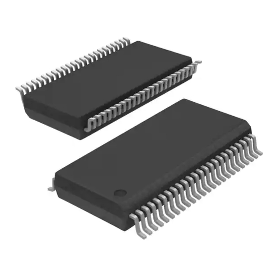
48-pin 300-mil SSOP Package (RoHS-Compliant)
■
Logic Block Diagram
Cypress Semiconductor Corporation
Document #: 001-52039 Rev. **
A
5
A
6
A
7
A
8
STATIC RAM
A
9
ARRAY
A
12
1024 X 1024
A
13
A
14
A
15
A
16
DQ
0
COLUMN I/O
DQ
1
DQ
COLUMN DEC
2
DQ
3
DQ
4
DQ
A
A
A
5
0
1
2
DQ
6
DQ
7
•
198 Champion Court
128k X 8 AutoStore™ nvSRAM
with Real Time Clock
Description
The Cypress STK17TA8 combines a 1 Mb nonvolatile static RAM
(nvSRAM) with a full featured real time clock in a reliable,
monolithic integrated circuit.
The 1 Mb nvSRAM is a fast static RAM with a nonvolatile
Quantum Trap storage element included with each memory cell.
The SRAM provides the fast access and cycle times, ease of use
and unlimited read and write endurance of a normal SRAM. Data
transfers automatically to the nonvolatile storage cells when
power loss is detected (the STORE operation). On power up,
data is automatically restored to the SRAM (the RECALL
operation). Both STORE and RECALL operations are also
available under software control.
The real time clock function provides an accurate clock with leap
year tracking and a programmable, high accuracy oscillator. The
Alarm function is programmable for one-time alarms or periodic
minutes, hours, or days alarms. There is also a programmable
watchdog timer for processor control.
V
CC
Quantum Trap
1024 X 1024
POWER
CONTROL
STORE
STORE/
RECALL
RECALL
CONTROL
A
A
A
A
3
4
10
11
,
•
San Jose
CA 95134-1709
STK17TA8
V
CAP
V
RTCbat
V
RTCcap
HSB
SOFTWARE
A
– A
15
0
DETECT
X
1
RTC
X
2
INT
A
– A
MUX
16
0
G
E
W
•
408-943-2600
Revised March 02, 2009
[+] Feedback
Advertisement
Table of Contents

Related Manuals for Cypress AutoStore STK17TA8


Summary of Contents for Cypress AutoStore STK17TA8
- Page 1 Features nvSRAM Combined with Integrated Real Time Clock Functions ■ (RTC, Watchdog Timer, Clock Alarm, Power Monitor) Capacitor or Battery Backup for RTC ■ 25, 45 ns Read Access and Read/Write Cycle Time ■ Unlimited Read/Write Endurance ■ Automatic nonvolatile STORE on Power Loss ■...
-
Page 2: Pin Descriptions
Pinouts Figure 1. Pin Diagram - 48-PIn SSOP (TOP) RTCbat Pin Descriptions Pin Name IO Type Input Address: The 17 address inputs select one of 131,072 bytes in the nvSRAM array or one of 16 bytes in the clock register map Data: Bi-directional 8-bit data bus for accessing the nvSRAM and RTC Input Chip Enable: The active low E input selects the device... -
Page 3: Absolute Maximum Ratings
Absolute Maximum Ratings Voltage on Input Relative to Ground ...–0.1V to 4.1V Voltage on Input Relative to V ...–0.5V to (V Voltage on DQ or HSB...–0.5V to (V Temperature under Bias ... –55°C to 125°C Junction Temperature ... –55°C to 140°C Storage Temperature ... -
Page 4: Ac Test Conditions
DC Electrical Characteristics = 2.7V-3.6V) Symbol Parameter Operating Temperature Operating Voltage Storage Capacitance Nonvolatile STORE operations DATA Data Retention AC Test Conditions Input Pulse Levels ...0V to 3V Input Rise and Fall Times ... <5 ns Input and Output Timing Reference Levels ... 1.5V Output Load...See Figure 2 Capacitance... - Page 5 RTC DC Characteristics Symbol Parameter RTC Backup Current RTC Battery Pin Voltage RTCbat RTC Capacitor Pin Voltage RTCcap RTC Oscillator time to start OSCS Figure 4. RTC Recommended Component Configuration Document #: 001-52039 Rev. ** Commercial Industrial Units — — —...
- Page 6 SRAM READ Cycles #1 and #2 Symbols Alt. Chip Enable Access Time ELQV Read Cycle Time AVAV ELEH Address Access Time AVQV AVQV Output Enable to Data Valid GLQV Output Hold after Address Change AXQX AXQX Address Change or Chip Enable to Output Active ELQX Address Change or Chip Disable to Output EHQZ...
- Page 7 SRAM WRITE Cycles #1 and #2 Symbols Alt. AVAV AVAV WLWH WLEH ELWH ELEH DVWH DVEH WHDX EHDX AVWH AVEH AVWL AVEL WHAX EHAX 5, 7 WLQZ WHQX Figure 7. SRAM WRITE Cycle #1: W Controlled ADDRESS AVWL DATA IN DATA IN DATA OUT PREVIOUS DATA...
- Page 8 AutoStore/Power Up Recall Symbols Standard Alternate Power-up RECALL Duration HRECALL STORE Cycle Duration STORE HLHZ Low Voltage Trigger Level SWITCH CCRISE NOTE Read and Write cycles will be ignored during STORE, RECALL and while V Notes 9. t starts from the time V rises above V HRECALL 10.
- Page 9 Software-Controlled STORE/RECALL Cycle In the following table, the software controlled STORE and RECALL cycle parameters are listed. Symbols E Cont G Cont Alternate 26 t AVAV AVAV 27 t AVEL AVGL 28 t ELEH GLGH 29 t EHAX GHAX 30 t RECALL RECALL Figure 10.
- Page 10 Hardware STORE Cycle Symbols Standard Alternate Hardware STORE to SRAM Disabled DELAY HLQZ Hardware STORE Pulse Width HLHX Soft Sequence Commands Symbols Standard Soft Sequence Processing Time Notes 14. On a hardware STORE initiation, SRAM operation continues to be enabled for time tDELAY to allow READ/WRITE cycles to compete. 15.
-
Page 11: Mode Selection
MODE Selection Notes 17. The six consecutive addresses must be in the order listed. W must be high during all six consecutive cycles to enable a nonvolatile cycle. 18. While there are 17 addresses on the STK17TA8, only the lower 16 are used to control software modes 19. - Page 12 nvSRAM Operation The STK17TA8 nvSRAM is made up of two functional compo- nents paired in the same physical cell. These are the SRAM memory cell and a nonvolatile QuantumTrap cell. The SRAM memory cell operates like a standard fast static RAM. Data in the SRAM can be transferred to the nonvolatile cell (the STORE operation), or from the nonvolatile cell to SRAM (the RECALL operation).
-
Page 13: Noise Considerations
atile elements. Once a STORE cycle is initiated, further memory inputs and outputs are disabled until the cycle is completed. To initiate the Software STORE cycle, the following read sequence must be performed: 1. Read Address 0x4E38 Valid READ 2. Read Address 0xB1C7 Valid READ 3. - Page 14 Figure 15. Current versus Cycle Time RTC Operations Real Time Clock The clock registers maintain time up to 9,999 years in one second increments. The user can set the time to any calendar time and the clock automatically keeps track of days of the week and month, leap years, and century transitions.
-
Page 15: Power Monitor
Calibrating The Clock The RTC is driven by a quartz controlled oscillator with a nominal frequency of 32.768 KHz. Clock accuracy will depend on the quality of the crystal, specified (usually 35 ppm at 25 C). This error could equate to 1.53 minutes gain or loss per month. The STK17TA8 employs a calibration circuit that can improve the accuracy to +1/-2 ppm at 25 C. - Page 16 Interrupts The STK17TA8 has a Flags register, Interrupt Register, and interrupt logic that can interrupt a microcontroller or generate a power-up master reset signal. There are three potential interrupt sources: the watchdog timer, the power monitor, and the clock alarm. Each can be individually enabled to drive the INT pin by setting the appropriate bit in the Interrupt register.
- Page 17 RTC Register Register 0x1FFFF 10s Years 0x1FFFE 0x1FFFD 0x1FFFC 0x1FFFB 0x1FFFA 10s Minutes 0x1FFF9 10s Seconds 0x1FFF8 OSCEN 0x1FFF7 0x1FFF6 WIE [0] AIE [0] 0x1FFF5 0x1FFF4 0x1FFF3 10 Alarm Minutes 0x1FFF2 10 Alarm Seconds 0x1FFF1 10s Centuries 0x1FFF0 * A binary value, not a BCD value. 0 - Not implemented, reserved for future use.
- Page 18 Register Map Detail 0x1FFFF 10s Years Contains the lower two BCD digits of the year. Lower nibble contains the value for years; upper nibble contains the value for 10s of years. Each nibble operates from 0 to 9. The range for the register is 0-99. 0x1FFFE Contains the BCD digits of the month.
- Page 19 Register Map Detail (continued) 0x1FFF7 Watchdog Strobe. Setting this bit to 1 reloads and restarts the watchdog timer. The bit is cleared automatically once the watchdog timer is reset. The WDS bit is write only. Reading it always will return a 0. Watchdog Write Enable.
- Page 20 Register Map Detail (continued) 0x1FFF2 Contains the alarm value for the seconds and the mask bit to select or deselect the seconds’ value. Match. Setting this bit to 0 causes the seconds’ value to be used in the alarm match. Setting this bit to 1 causes the match circuit to ignore the seconds value.
-
Page 21: Ordering Information
Ordering Information STK17TA8-R F 45 ITR Ordering Codes Ordering Code STK17TA8-RF25 3V 128Kx8 AutoStore nvSRAM+RTC SSOP48-300 STK17TA8-RF45 3V 128Kx8 AutoStore nvSRAM+RTC SSOP48-300 STK17TA8-RF25TR 3V 128Kx8 AutoStore nvSRAM+RTC SSOP48-300 STK17TA8-RF45TR 3V 128Kx8 AutoStore nvSRAM+RTC SSOP48-300 STK17TA8-RF25I 3V 128Kx8 AutoStore nvSRAM+RTC SSOP48-300 STK17TA8-RF45I 3V 128Kx8 AutoStore nvSRAM+RTC SSOP48-300 STK17TA8-RF25ITR 3V 128Kx8 AutoStore nvSRAM+RTC SSOP48-300... -
Page 22: Package Diagrams
STK17TA8 Package Diagrams Figure 17. 48-Pin SSOP (51-85061) 51-85061 *C Document #: 001-52039 Rev. ** Page 22 of 23 [+] Feedback... - Page 23 Document History Page Document Title: STK17TA8 128k X 8 AutoStore™ nvSRAM with Real Time Clock Document Number: 001-52039 Orig. of Submission Rev. ECN No. Change 2668660 GVCH/PYRS 03/04/2009 Sales, Solutions, and Legal Information Worldwide Sales and Design Support Cypress maintains a worldwide network of offices, solution centers, manufacturer’s representatives, and distributors. To find the office closest to you, visit us at cypress.com/sales.
Need help?
Do you have a question about the AutoStore STK17TA8 and is the answer not in the manual?
Questions and answers