Table of Contents
Advertisement
Quick Links
cPCI-FRM11
User Manual
Version 1.1
ⓒ 2005 DAQ SYSTEM Co., Ltd. All rights reserved.
Microsoft® is a registered trademark; Windows®, Windows NT®, Windows XP®, Windows 7®, Windows 8®, Windows 10®
All other trademarks or intellectual property mentioned herein belongs to their respective owners.
Information furnished by DAQ SYSTEM is believed to be accurate and reliable, However, no responsibility is assumed by DAQ SYSTEM for its use, nor
for any infringements of patents or other rights of third parties which may result from its use. No license is granted by implication or otherwise under
any patent or copyrights of DAQ SYSTEM.
The information in this document is subject to change without notice and no part of this document may be copied or reproduced without the prior
written consent.
Advertisement
Table of Contents

Related Manuals for DAQ system cPCI-FRM11


Summary of Contents for DAQ system cPCI-FRM11
- Page 1 All other trademarks or intellectual property mentioned herein belongs to their respective owners. Information furnished by DAQ SYSTEM is believed to be accurate and reliable, However, no responsibility is assumed by DAQ SYSTEM for its use, nor for any infringements of patents or other rights of third parties which may result from its use. No license is granted by implication or otherwise under any patent or copyrights of DAQ SYSTEM.
-
Page 2: Table Of Contents
2. cPCI-FRM11 Board Function 2-1 Board Block Diagram ------------------------------------------------------------------ 2-2 Camera Link ----------------------------------------------------------------- 2-3 Camera Link Cable & Connector ----------------------------------------------------------- 2-4 Camera Link & cPCI-FRM11 ---------------------------------------------------------- 3. cPCI-FRM11 Board Description Board Layout ------------------------------------------------------------------------ 3-2 Device Features ------------------------------------------------------------------------ 13 3-3 Connector Pin out... - Page 3 User‟s Manual 5. Sample Program 5-1 FrmTest Program ---------------------------------------------------------------- 5-1-1 Image Frame Function ------------------------------------------------------ 5-1-2 UART Function ---------------------------------------------------------------- 5-1-3 DIO Function ---------------------------------------------------------------- 6. Test 6-1 Image Frame Input Test ------------------------------------------------------------------ 6-2 UART Tx/Rx Test -------------------------------------------------------------------- DIO Test ------------------------------------------------------------------- Appendix...
-
Page 4: Introduction
The operation of the board is controlled by program API, figure [1-1] shows connection of the system. [Figure 1-1. cPCI-FRM11 Board Usage As shown in Figure [1-1], the cPCI-FRM11 is inserted into any available PCI slots in the Compact PCI system. It receives image frame from camera via Camera-Link Standard Interface. And, received data... -
Page 5: Product Features
User‟s Manual 1-1 Product Features Items Description Remark Hardware PC Interface Compact PCI 32bit/33MHz PCI Bus Interface Operation Power +5V Single Power operation Max within 300mA Video Interface Base Camera Link Feature Area Scan Camera Pixel Clock : 20 ~ 85MHz External I/O 8-Ch. -
Page 6: Product Application
User‟s Manual 1-2 Product Applications Image recognition (Pattern, particle, etc.) Inspection equipment (Sensor, Semiconductor, Device etc.) Black and White, Color Image Display Medical Image Capture (X-ray, Supersonic etc.) ... -
Page 7: Cpci-Frm11 Board Function
2. cPCI-FRM11 Board Function 2-2 Board Block Diagram As shown in the figure below, in the case of cPCI-FRM11, FPGA Core Logic is in charge of overall control. Main functions include Frame Data reception, UART data transmission/reception for this purpose, and Camera Control signal output. -
Page 8: Camera Link
User‟s Manual 2-2 Camera Link Camera Link is a communication interface developed for use in vision applications. In the past, we used proprietary connectors and cables between camera makers and frame grabber makers. This caused a lot of confusion and cost increase for users. In order to resolve this confusion,... - Page 9 User‟s Manual [Figure 2-2. Base Camera Link Block Diagram]...
-
Page 10: Camera Link Cable & Connector
User‟s Manual 2-3 Camera Link Cable & Connector Camera Link The connection between the camera and the cPCI-FRM11 board uses a 26 Pin MDR (Mini D Ribbon) cable. The camera link cable consists of a twin-axial shielded cable and two MDR 26-male plugs. -
Page 11: Camera Link & Cpci-Frm11
(Frame Valid, Line Valid, Data Valid, and a spare) through the Channel Link chip in cPCI-FRM11. In addition, a clock signal is made with one LVDS to synchronize the signal between the camera and cPCI-FRM11, and the remaining cameras control signals and communication signals are converted into general TTL signal levels and used. - Page 12 User‟s Manual The figure below shows the circuit that uses the serial input signal input through the Camera- link cable as a general input on the cPCI-FRM11 board. [Figure 2-7. Serial Communication LVDS Digital Output Circuit] cPCI-FRM11 supports Base Configuration including the following bit allocation.
-
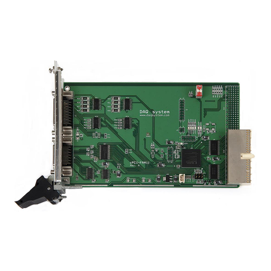
Page 13: Cpci-Frm11 Board Description
User‟s Manual 3. cPCI-FRM11 Board Description In this chapter, the primary functions of the cPCI-FRM11 board are described briefly. For more information, refer to the device specification. 3-1 cPCI-FRM11 Board Layout [Figure 3-1. cPCI-FRM11 Layout] The board has seven LEDs to indicate the operation status. -
Page 14: Device Features
User‟s Manual 3-2 Device Features (1) FPGA : U5 All of the board functions are controlled by the Logic program of the FPGA. (2) LVDS : U4, U9 Receive Image frame through LVDS interface. UART signal Receive/Transmit through LVDS interface. -
Page 15: Connector Pin Out
User‟s Manual 3-3 Connector Pin-out This section describes the connectors and jumpers used in cPCI-FRM11. As for main connectors, there are MDR 26pin connector for Camera Link connection and MDR 36pin connector for external digital input/output connection port. [Figure 3-2] shows the bracket that interfaces with the board and the outside, and the connection connector. -
Page 16: J1(Mdr36) Connector
User‟s Manual 3-3-1 J1 (MDR36) Connector [Table 1] below shows the pin map of the J1 (MDR36) connector of the board. [Figure 3-3. cPCI-FRM11 J1 Connector Pin-out]... - Page 17 User‟s Manual [Table 1. J1 Connector] Pin No. Name Description STX+ LINE TRIGGER OUT+ SRX+ LINE TRIGGER IN+ +12V +12V 3.3V 3.3V DOUT_COM1 OUTPUT COMMON 1 (FOR output 4,5,6,7) DOUT OUTPUT 7 DOUT OUTPUT 6 DOUT OUTPUT 5 DOUT...
- Page 18 User‟s Manual In cPCI-FRM11 board, 8 digital inputs and 8 digital outputs isolated by photo-couplers can be used through J1 connector. The circuit is shown in [Figure 3-4]. 2.4K DIN7..4 IN7..4 DIN_COM1 2.4K DIN3..0 IN3..0 DIN_COM0 < Photo coupler input>...
-
Page 19: J5(Mdr26) Connector
Camera Link standard, so please refer to the Camera Link standard document for details. Frame Grabber Inner shield Inner shield Xclk- Xclk+ SerTC+ SerTC- SerTFG- SerTFG+ CC1- CC1+ CC2+ CC2- CC3- CC3+ CC4+ CC4- Inner shield Inner shield [Figure 3-5. cPCI-FRM11 J5 Connector Pin-out]... - Page 20 User‟s Manual [Table 1. J5 Connector] Pin No. Name Description Remark Inner Shield Cable shield CC4- Camera Control output 4- CC3+ Camera Control output 3+ CC2-- Camera Control output 2- CC1+ Camera Control output 1+ SerTFG+ Serial to Frame grabber +...
-
Page 21: Sw1 Switch
User‟s Manual 3-3-3 SW1 Switch cPCI-FRM11 board is designed to use up to 4 cPCI-FRM11 boards simultaneously in one system (PC). Each board classification can be set through the 4-pin DIP switch in the board. [Figure 3-6. SW1 Switch (Top View)] [Table 4. -
Page 22: Installation
The board environment must be Windows 2000 SP4 or higher and Windows XP SP1 or higher. First, turn off the PC's power, plug the cPCI-FRM11 board into the Compact PCI Slot, and turn on the PC's power. When the “Start New Hardware Wizard” window opens as shown below, selects it... - Page 23 User‟s Manual 1. Select as below and click the Next button 2. Select Driver from the enclosed CD and click the Next button.
- Page 24 User‟s Manual 3. Click the Next button. It indicates that the installation process is proceeding as shown below. The driver folder contains “pci_frm11.inf” and “pci_frm11.sys” files required for driver installation. Click Next to install the driver files. 4. When the installation is completed normally, it is shown in the figure below.
- Page 25 7. If it appears as shown in the figure below, the installation has been completed normally. The above figure shows the screen where the cPCI-FRM11 board is normally installed in the PC. (Note) cPCI-FRM11 board is registered as a PCIe-FRM11 device to maintain compatibility with the existing PCIe-FRM11 board.
-
Page 26: Sample Program
User‟s Manual 5. Sample Program In the CDROM folder provided with the board, a sample program is provided for easy use of the board. First of all, “FrmTest.exe”, one of the executable files, displays Frame Data as a hexadecimal value and stores it in memory or hard disk so that developers can utilize the necessary frame data. -
Page 27: Image Frame Function
User‟s Manual folder or the folder specified by the Path environment variable. 5-1-1 Image Frame Function (1) „DXD810/DXD1417’ Combo-box Use this box to set up the operation mode. (2) „LVDS Init’ button Press this button to initialize the function of receiving image frame data. It is performed only once after power is applied to the board. -
Page 28: Dio Function
User‟s Manual (5) „Stop Timer’ button Press this button to stop the timer. (6) „UART Init’ button Press this button to initialize UART. It must be performed only once after power is applied to the board. (7) „UART Close’ button Press this button to finish usage of the board and terminate the program. -
Page 29: Test
“FrmTest.exe”. [Figure 6-1. Equipment Connection for Testing] In the figure above, the cPCI-FRM11 board is installed in the PC, but the figure is drawn outside for better understanding. The image frame simulator uses a self-made one by the DAQ system, and if you have an actual device, you can use it. -
Page 30: Uart Tx/Rx Test
User‟s Manual (1) After initializing by pressing the “LVDS init” button, click the “Start” button to save the image frame. Press the “Frame Read” button to load the image data of the program. The read data is displayed in the editor box, so check whether it matches the actual data sent. In some cases, a separate verification program must be used, so press the “Save to”... -
Page 31: Appendix
User‟s Manual Appendix Board Size The external sizes of the board are as follows. For detailed dimensions, please contact the person in charge. -
Page 32: Repair Regulations
⑥ Products whose serial number has been changed or removed intentionally ⑦ If DAQ SYSTEM determines that it is the customer's fault for other reasons (5) Shipping costs for returning the repaired product to DAQ SYSTEM are the responsibility of the customer. -
Page 33: References
User‟s Manual References 1. Specification of Camera Link Interface Standard for Digital Cameras and Frame Grabbers -- Camera Link committee 2. PCI Local Bus Specification Revision2.1 -- PCI Special Interest Group 3. AN201 How to build application using API -- DAQ system 4. - Page 34 User‟s Manual MEMO Contact Point Web sit : https://www.daqsystem.com Email : postmaster@daqsystem.com...
Need help?
Do you have a question about the cPCI-FRM11 and is the answer not in the manual?
Questions and answers