Advertisement
Quick Links
3.5" SBC Supports Intel® Alder Lake-P Processor, Dual HDMI,
Dual DP, Dual 2.5GbE, M.2 A Key + B Key + M Key, USB 3.2 Gen 2,
SATA 6Gb/s, COM, PCIe x4 for Riser Card and RoHS
Quick Installation Guide
Package List
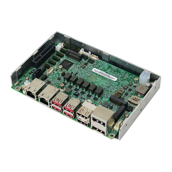
WAFER-ADL-P package includes the following items:
1 x WAFER-ADL-P single board computer with heat spreader
1 x SATA with power cable
1 x Power cable
1 x QIG
WAFER-ADL-P
Version 1.0
May 25, 2023
©2023 Copyright by IEI Integration Corp.
All rights reserved.
Advertisement

Related Manuals for IEI Technology WAFER-ADL-P


Summary of Contents for IEI Technology WAFER-ADL-P
- Page 1 Quick Installation Guide Version 1.0 May 25, 2023 Package List WAFER-ADL-P package includes the following items: 1 x WAFER-ADL-P single board computer with heat spreader 1 x SATA with power cable 1 x Power cable 1 x QIG ©2023 Copyright by IEI Integration Corp.
-
Page 2: Specifications
Specifications CPU: 12th Gen. Intel® mobile Alder Lake-P on board SoC Memory: On-board 8GB 3200 MHz LPDDR4x memory BIOS: AMI UEFI BIOS Graphics Engine: Intel® UHD Graphics for Celeron® 7305 and Core™ i3-1215U Intel® Xe Graphics architecture for Core™ i5-1235U and Core™ i7-1255U Display Output: ... - Page 3 Weight: GW:850 g / NW:350 g IEI Resource Download Center All the drivers and utility for the https://download.ieiworld.com WAFER-ADL-P are available on IEI Resource Download Center. Type WAFER-ADL-P and press Enter to find all the relevant software, utilities, and documentation. To install...
-
Page 4: Ordering Information
Ordering Information WAFER-ADL-P-i7C-R10: 3.5" SBC supports Intel® Alder Lake-P Core™ i7-1255U processor, with 8GB LPDDR4x memory on board, dual DP, dual HDMI, dual 2.5 GbE, USB 3.2 Gen 2 , M.2, SATA 6Gb/s, COM, PCIe x4 for riser card and RoHS ... -
Page 5: Jumpers Setting And Connectors
Jumpers Setting and Connectors LABEL FUNCTION J_ATX_AT1 AT/ATX power mode setting J_CMOS1 Clear CMOS button ME_FLASH1 Flash descriptor security override jumper J_AUDIO1 Audio connector for IEI AC-KIT-888S kit PWR1 12V power input connector BAT1 RTC battery connector Buzzer connector J_CHASSIS1 Chassis intrusion connector J_DIO1 Digital I/O connector... - Page 6 J_ATX_AT1: AT/ATX Power Mode Setting PIN NO. DESCRIPTION Short A - B ATX Power Mode (default) Short B - C AT Power Mode J_CMOS1: Clear CMOS Button Status DESCRIPTION Keep CMOS Setup (Normal Operation) Press Clear CMOS Setup ME_FLASH1: Flash Descriptor Security Override Jumper PIN NO.
- Page 7 BAT1: RTC Battery Connector PIN NO. DESCRIPTION PIN NO. DESCRIPTION VBATT SP1: Buzzer Connector PIN NO. DESCRIPTION PIN NO. DESCRIPTION PC_BEEP_N J_CHASSIS1: Chassis Intrusion Connector PIN NO. DESCRIPTION PIN NO. DESCRIPTION CASEOPEN_N J_DIO1 : Digital Input/Output Connector PIN NO. DESCRIPTION PIN NO.
- Page 8 F_PANEL1: Front Panel Connector PIN NO. DESCRIPTION PIN NO. DESCRIPTION PWR_LED- HDD_LED+ PWR_LED+ HDD_LED- J_I2C1: I C Connector PIN NO. DESCRIPTION PIN NO. DESCRIPTION SMB_CLK_EC SMB_DATA_EC PWR_BTN1: Power Button Connector DESCRIPTION DESCRIPTION PWRBTN_SW# RST_BTN1: Reset Button Connector DESCRIPTION DESCRIPTION EXTRST- COM1, COM2, COM3, COM4: RS-232 Serial Port Connectors PIN NO.
- Page 9 COM5, COM6: RS-232/422/485 Serial Port Connectors PIN NO. DESCRIPTION PIN NO. DESCRIPTION SATA1: SATA 6Gb/s Connector PIN NO. DESCRIPTION PIN NO. DESCRIPTION SATA_RX‐ SATA_TX+ SATA RX+ SATA_TX‐ SATA_PWR1:SATA Power Connector PIN NO. DESCRIPTION PIN NO. DESCRIPTION VCC5V J_SMB1: SMBus Connector PIN NO.
- Page 10 EC_SPI1: Flash EC ROM Connector PIN NO. DESCRIPTION PIN NO. DESCRIPTION VCC3.3V MISO HOLD DET# MOSI USB2_1, USB2_2: Internal USB 2.0 Connectors PIN NO. DESCRIPTION PIN NO. DESCRIPTION USB_DATA- USB_DATA+ USB_DATA+ USB_DATA- J1: MP2960GQKT FW Flash Connector PIN NO. DESCRIPTION PIN NO.
- Page 11 PCIE_TX_DP PCIE_TX_DN WLAN_CL_RST_N WLAN_CL_DATA PCIE_RX_DP WLAN_CL_CLK PCIE_RX_DN PCIE_CLK+ PCIE_CLK- SLOT_RST +3.3V M.2_A_WAKE +3.3V +3.3V +3.3V M2_B1: M.2 3042 B Key Slot PIN NO. DESCRIPTION PIN NO. DESCRIPTION +V3.3 +V3.3 USB2_DP W_DISABLE_N...
- Page 12 USB2_DN Module Key Module Key Module Key Module Key Module Key Module Key Module Key Module Key M.2_B_WAKE PCIE_1_RX_DN SIM_RST PCIE_1_RX_DP SIM_CLK SIM_CIO PCIE_1_TX_DN SIM_VCC PCIE_1_TX_DP PCIE_0_RX_DN PCIE_0_RX_DP PCIE_0_TX_DN PCIE_0_TX_DP SLOT_RST PCIE_CLK_DN M.2_B_WAKE PCIE_CLK_DP +V3.3 +V3.3 +V3.3...
- Page 13 M2_M1: M.2 2242/2280 M Key Slot PIN NO. DESCRIPTION PIN NO. DESCRIPTION +V3.3 +V3.3 PCIE_3_RX_DN PCIE_3_RX_DP NGFF1_ACT_N PCIE_3_TX_DN +V3.3 PCIE_3_TX_DP +V3.3 +V3.3 PCIE_2_RX_DN +V3.3 PCIE_2_RX_DP PCIE_2_TX_DN PCIE_2_TX_DP PCIE_1_RX_DN PCIE_1_RX_DP PCIE_1_TX_DN PCIE_1_TX_DP M_2_SSD_SLP PCIE_0_RX_DN PCIE_0_RX_DP PCIE_0_TX_DN PCIE_0_TX_DP SLOT_RST PCIE_CLK_DN PCIE_CLK_DP Module Key Module Key Module Key Module Key...
- Page 14 +V3.3 +V3.3 +V3.3 SIM1: SIM Card Slot PIN NO. DESCRIPTION PIN NO. DESCRIPTION SIM_VCC SIM_RST SIM_CLK SIM_CIO DP1: External Dual DisplayPort Connector PIN NO. DESCRIPTION PIN NO. DESCRIPTION LANE0P LANE3N LANE0N CONFIG_A_1 LANE1P CONFIG_A_2 AUXP LANE1N LANE2P AUXN LANE2N LANE3P...
- Page 15 HDMI1: External Dual HDMI Connector PIN NO. DESCRIPTION PIN NO. DESCRIPTION HDMI_DATA2P HDMI_CLKN HDMI_DATA2N HDMI_DATA1P HDMI_CLK HDMI_DATA1N HDMI_SDA HDMI_DATA0P HDMI_DATA0N HDMI_HPD HDMI_CLKP USB3_1, USB3_2: External Dual USB 3.2 Gen 2 Connector PIN NO. DESCRIPTION PIN NO. DESCRIPTION USB_DATA- USB_DATA- USB_DATA+ USB_ DATA+ USB3_RX- USB3_RX-...
- Page 16 Board Layout: Jumper and Connector Locations (Unit: mm)
Need help?
Do you have a question about the WAFER-ADL-P and is the answer not in the manual?
Questions and answers