IEI Technology WAFER-PV-D5252 User Manual
3.5" sbc with intel atom processor
up to 2.0 gb ddr3, vga, lvds, pcle mini, rs-232/422/485, sata 3gb/s, compactflash, eigh usb, rohs
Hide thumbs
Also See for WAFER-PV-D5252:
- User manual (116 pages) ,
- User manual (142 pages) ,
- User manual (116 pages)
Table of Contents
Advertisement
Quick Links
Advertisement
Table of Contents

Subscribe to Our Youtube Channel
Related Manuals for IEI Technology WAFER-PV-D5252


Summary of Contents for IEI Technology WAFER-PV-D5252
- Page 1 WAFER-PV-D5252/D4252/N4552 SBC IEI Technology Corp. MODEL: WAFER-PV-D5252/D4252/N4552 3.5" SBC with Intel® Atom™ Processor Up to 2.0 GB DDR3, VGA, LVDS, PCIe Mini, RS-232/422/485, SATA 3Gb/s, CompactFlash®, Eight USB, RoHS User Manual Page i Rev. 1.02 – 20 March, 2013...
- Page 2 WAFER-PV-D5252/D4252/N4552 SBC Revision Date Version Changes 20 March, 2013 1.02 Modified supported memory specifications (Table 1-1) 4 March, 2011 1.01 Modified LVDS connector pinouts (Table 3-11) Modified LVDS resolution select jumper settings (Table 4-5) 11 January, 2011 1.00 Initial release...
- Page 3 WAFER-PV-D5252/D4252/N4552 SBC Copyright COPYRIGHT NOTICE The information in this document is subject to change without prior notice in order to improve reliability, design and function and does not represent a commitment on the part of the manufacturer. In no event will the manufacturer be liable for direct, indirect, special, incidental, or consequential damages arising out of the use or inability to use the product or documentation, even if advised of the possibility of such damages.
-
Page 4: Table Of Contents
WAFER-PV-D5252/D4252/N4552 SBC Table of Contents 1 INTRODUCTION......................1 1.1 I ......................2 NTRODUCTION 1.2 B ........................2 ENEFITS 1.3 F ........................3 EATURES 1.4 C ......................3 ONNECTORS 1.5 D ....................... 4 IMENSIONS 1.6 D ........................ 6 1.7 T ..................7... - Page 5 WAFER-PV-D5252/D4252/N4552 SBC 3.2.11 PCIe Mini Card Slot..................25 3.2.12 Power Button Connector................27 3.2.13 Reset Button Connector ................. 27 3.2.14 RS-232/422/485 Serial Port Connector (COM2) .......... 28 3.2.15 RS-232 Serial Port Connector (COM3~COM6)..........29 3.2.16 SATA Drive Connectors ................. 30 3.2.17 SATA Power Connectors ................
- Page 6 WAFER-PV-D5252/D4252/N4552 SBC 4.7.2 Audio Kit Installation..................52 4.7.3 Keyboard/Mouse Connector ................54 4.7.4 Four Serial Port Connector ................56 4.8 E ........... 57 XTERNAL ERIPHERAL NTERFACE ONNECTION 4.8.1 LAN Connection (Single Connector) ............... 57 4.8.2 Serial Device Connection ................58 4.8.3 USB Connection (Dual Connector) ..............
- Page 7 WAFER-PV-D5252/D4252/N4552 SBC A BIOS OPTIONS ......................91 B ONE KEY RECOVERY ..................... 94 B.1 O ..............95 ECOVERY NTRODUCTION B.1.1 System Requirement..................96 B.1.2 Supported Operating System ................97 B.2 S ................98 ETUP ROCEDURE FOR INDOWS B.2.1 Hardware and BIOS Setup ................98 B.2.2 Create Partitions .....................
- Page 8 WAFER-PV-D5252/D4252/N4552 SBC List of Figures Figure 1-1: WAFER-PV-D5252/D4252/N4552................2 Figure 1-2: Connectors ........................3 Figure 1-3: Dimensions without Heatsink (mm) ................4 Figure 1-4: Dimensions with Heatsink (mm)................5 Figure 1-5: Data Flow Diagram......................6 Figure 3-1: Connector and Jumper Locations................14 Figure 3-2: ATX Power Connector Location ................17 Figure 3-3: Audio Connector Location ..................17...
- Page 9 WAFER-PV-D5252/D4252/N4552 SBC Figure 3-26: VGA Connector .......................38 Figure 4-1: SO-DIMM Installation ....................42 Figure 4-2: CompactFlash® Card Installation ................43 Figure 4-3: AT/ATX Mode Selection Jumper Location..............45 Figure 4-4: Clear CMOS Jumper Location .................46 Figure 4-5: LVDS Voltage Selection Jumper Location .............47 Figure 4-6: LVDS Resolution Selection Jumper Location............48...
- Page 10 WAFER-PV-D5252/D4252/N4552 SBC Figure B-14: Select a Local Source Drive ................107 Figure B-15: Select a Source Partition from Basic Drive ............107 Figure B-16: File Name to Copy Image to ................108 Figure B-17: Compress Image....................108 Figure B-18: Image Creation Confirmation ................109 Figure B-19: Image Creation Process..................
- Page 11 WAFER-PV-D5252/D4252/N4552 SBC List of Tables Table 1-1: Technical Specifications....................8 Table 2-1: Packing List.........................12 Table 2-2: Optional Items......................12 Table 3-1: Peripheral Interface Connectors ................16 Table 3-2: Rear Panel Connectors ....................16 Table 3-3: ATX Power Connector Pinouts .................17 Table 3-4: Audio Connector Pinouts ..................18 Table 3-5: Battery Connector Pinouts ..................18...
- Page 12 WAFER-PV-D5252/D4252/N4552 SBC Table 4-1: Jumpers ........................44 Table 4-2: AT/ATX Mode Selection .....................45 Table 4-3: Clear CMOS Jumper Settings..................46 Table 4-4: LVDS Voltage Selection .....................47 Table 4-5: LVDS Resolution Selection..................47 Table 4-6: CompactFlash® Master/Slave Selection ..............48 Table 4-7: COM3 RS-232/422/485 Selection ................49 Table 4-8: COM 1 Pin 9 Setting Jumper Settings ..............50...
- Page 13 WAFER-PV-D5252/D4252/N4552 SBC BIOS Menus BIOS Menu 1: Main ........................66 BIOS Menu 2: Advanced ......................67 BIOS Menu 3: ACPI Configuration ....................68 BIOS Menu 4: CPU Configuration ....................69 BIOS Menu 5: IDE Configuration....................70 BIOS Menu 6: USB Configuration ....................71 BIOS Menu 7: Super IO Configuration..................72 BIOS Menu 8: Serial Port n Configuration Menu...............73...
-
Page 14: Introduction
WAFER-PV-D5252/D4252/N4552 SBC Chapter Introduction Page 1... -
Page 15: Introduction
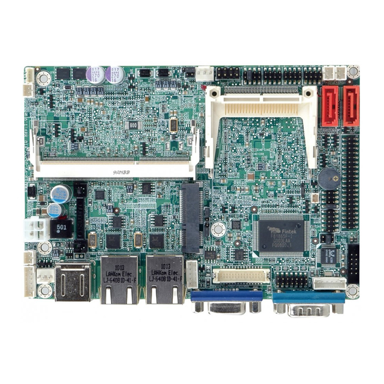
WAFER-PV-D5252/D4252/N4552 SBC 1.1 Introduction Figure 1-1: WAFER-PV-D5252/D4252/N4552 The WAFER-PV-D5252/D4252/N4552 is a 3.5" SBC with a Intel® Atom™ D525, D425 or N455 CPU. The WAFER-PV-D5252/D4252/N4552 is designed for fanless operation. The low power CPUs don't require active cooling and stay within specified heat range using the included heatsink. -
Page 16: Features
3.5" form factor Fanless design RoHS compliant Eight USB 2.0 ports Six serial ports PCIe Mini card slot CompactFlash® Type II slot Gigabit Ethernet 1.4 Connectors The connectors on the WAFER-PV-D5252/D4252/N4552 are shown in the figure below. Figure 1-2: Connectors Page 3... -
Page 17: Dimensions
WAFER-PV-D5252/D4252/N4552 SBC 1.5 Dimensions The main dimensions of the WAFER-PV-D5252/D4252/N4552 are shown in the diagram below. Figure 1-3: Dimensions without Heatsink (mm) Page 4... -
Page 18: Figure 1-4: Dimensions With Heatsink (Mm)
WAFER-PV-D5252/D4252/N4552 SBC Figure 1-4: Dimensions with Heatsink (mm) Page 5... -
Page 19: Data Flow
WAFER-PV-D5252/D4252/N4552 SBC 1.6 Data Flow Figure 1-5 shows the data flow between the system chipset, the CPU and other components installed on the motherboard. Figure 1-5: Data Flow Diagram Page 6... -
Page 20: Technical Specifications
WAFER-PV-D5252/D4252/N4552 SBC 1.7 Technical Specifications WAFER-PV-D5252/D4252/N4552 technical specifications are listed in Table 1-1. Specification WAFER-PV-D5252/D4252/N4552 Form Factor 3.5" Socket Embedded 1.8 GHz Intel® Atom™ D525 dual-core CPU with 1 MB L2 cache CPU Supported 1.8 GHz Intel® Atom™ D425 single-core CPU with 512 KB L2 cache 1.66 GHz Intel®... -
Page 21: Table 1-1: Technical Specifications
WAFER-PV-D5252/D4252/N4552 SBC I/O Interface Connectors Two 3-pin wafer for system fan Fan connector Keyboard/Mouse One internal 6-pin wafer connector Serial Ports Five RS-232 COM connectors One RS-232/422/485 COM connector USB 2.0/1.1 ports Six internal via pin header Two external USB ports... -
Page 22: Packing List
WAFER-PV-D5252/D4252/N4552 SBC Chapter Packing List Page 9... -
Page 23: Anti-Static Precautions
Only handle the edges of the PCB:- Don't touch the surface of the motherboard. Hold the motherboard by the edges when handling. 2.2 Unpacking Precautions When the WAFER-PV-D5252/D4252/N4552 is unpacked, please do the following: Follow the antistatic guidelines above. Make sure the packing box is facing upwards when opening. -
Page 24: Packing List
Contact the IEI reseller or vendor the WAFER-PV-D5252/D4252/N4552 was purchased from or contact an sales representative directly sending email sales@iei.com.tw. The WAFER-PV-D5252/D4252/N4552 is shipped with the following components: Quantity Item and Part Number Image WAFER-PV-D5252, WAFER-PV-D4252 or WAFER-PV-N4552 SATA and power cable... -
Page 25: Optional Items
WAFER-PV-D5252/D4252/N4552 SBC Quantity Item and Part Number Image Mini jumper pack (2.0mm) (P/N:33100-000033-RS) Utility CD Quick installation guide Table 2-1: Packing List 2.4 Optional Items These optional items are available. Item and Part Number Image Dual USB cable (wo bracket) -
Page 26: Connector Pinouts
WAFER-PV-D5252/D4252/N4552 SBC Chapter Connector Pinouts Page 13... -
Page 27: Peripheral Interface Connectors
WAFER-PV-D5252/D4252/N4552 SBC 3.1 Peripheral Interface Connectors Section 3.1.2 shows peripheral interface connector locations. Section 3.1.2 lists all the peripheral interface connectors seen in Section 3.1.2. 3.1.1 Layout The figure below shows the on-board peripheral connectors, rear panel peripheral connectors and on-board jumpers. -
Page 28: Peripheral Interface Connectors
WAFER-PV-D5252/D4252/N4552 SBC 3.1.2 Peripheral Interface Connectors The table below shows a list of the peripheral interface connectors on the WAFER-PV-D5252/D4252/N4552. Detailed descriptions of these connectors can be found below. Connector Type Label +12 V ATX power connector 4-pin connector Audio connector... -
Page 29: External Interface Panel Connectors
8-pin header USB2, USB3, USB4 Table 3-1: Peripheral Interface Connectors 3.1.3 External Interface Panel Connectors The table below lists the rear panel connectors on the WAFER-PV-D5252/D4252/N4552. Detailed descriptions of these connectors can be found in a later section. Connector Type Label... -
Page 30: Audio Connector
WAFER-PV-D5252/D4252/N4552 SBC Figure 3-2: ATX Power Connector Location Description Description Ground Ground +12 V +12V Table 3-3: ATX Power Connector Pinouts 3.2.2 Audio Connector CN Label: AUDIO1 CN Type: 10-pin header CN Location: See Figure 3-3 CN Pinouts: See Table 3-4 This connector connects to speakers, a microphone and an audio input. -
Page 31: Battery Connector
WAFER-PV-D5252/D4252/N4552 SBC Description Description GND_AUDIO GND_AUDIO MICIN MICIN Table 3-4: Audio Connector Pinouts 3.2.3 Battery Connector CN Label: BAT1 CN Type: 2-pin wafer CN Location: See Figure 3-4 CN Pinouts: See Table 3-5 This is connected to the system battery. The battery provides power to the system clock to retain the time when power is turned off. -
Page 32: Figure 3-5: Compactflash® Slot Location
WAFER-PV-D5252/D4252/N4552 SBC NOTE: 1. Both CompactFlash® Type I and Type II cards are supported. 2. To use SATA and CF, CF must be set to slave. A CompactFlash® Type I or Type II card can be used in this slot. -
Page 33: Digital I/O Connector
WAFER-PV-D5252/D4252/N4552 SBC Description Description CSEL# VS2# RESET# WAIT# INPACK# REG# BVD2 BVD1 IOCS16# CD2# GND2 Table 3-6: CompactFlash® Slot Pinouts 3.2.5 Digital I/O Connector CN Label: DIO1 10-pin header CN Type: CN Location: See Figure 3-6 CN Pinouts: See Table 3-7 The digital I/O connector provides programmable input and output for external devices. -
Page 34: Fan Connectors
WAFER-PV-D5252/D4252/N4552 SBC Description Description Output 3 Output 2 Output 1 Output 0 Input 3 Input 2 Input 1 Input 0 Table 3-7: Digital I/O Connector Pinouts 3.2.6 Fan Connectors CN Label: FAN1, FAN2 CN Type: 3-pin wafer CN Location: See Figure 3-7... -
Page 35: Keyboard/Mouse Connector
WAFER-PV-D5252/D4252/N4552 SBC 3.2.7 Keyboard/Mouse Connector CN Label: KB/MS1 6-pin wafer CN Type: CN Location: See Figure 3-8 CN Pinouts: See Table 3-9 The keyboard/mouse connector connects to a PS/2 Y-cable that can be connected to a PS/2 keyboard and mouse. -
Page 36: Lvds Connector
WAFER-PV-D5252/D4252/N4552 SBC CN Pinouts: See Table 3-10 The connector connects to the hard drive activity LED and power LED on the system front panel. +5 V power output is also provided via this connector. Figure 3-9: LED and +5 V Power Output Connector Location... -
Page 37: Lvds Backlight Connector
WAFER-PV-D5252/D4252/N4552 SBC Figure 3-10: LVDS Connector Location Description Description GND1 GND2 A_Y0 A_Y0# A_Y1 A_Y1# A_Y2 A_Y2# A_CK A_CK# GND3 GND4 GND5 GND6 VCC_LCD VCC_LCD VCC_LCD VCC_LCD Table 3-11: LVDS Connector Pinouts 3.2.10 LVDS Backlight Connector CN Label: INVERTER1 CN Type:... -
Page 38: Pcie Mini Card Slot
WAFER-PV-D5252/D4252/N4552 SBC CN Pinouts: See Table 3-12 The backlight inverter connector provides power to an LCD panel. Figure 3-11: Backlight Inverter Connector Description LCD_BKLTCTL GROUND +12V GROUND BACKLIGHT ENABLE Table 3-12: Backlight Inverter Connector 3.2.11 PCIe Mini Card Slot CN Label:... -
Page 39: Figure 3-12: Pcie Mini Card Slot Location
WAFER-PV-D5252/D4252/N4552 SBC Figure 3-12: PCIe Mini Card Slot Location Description Description PCIE_WAKE# VCC3 1.5V CLKREQ# LFRAME# LAD3 CLK- LAD2 CLK+ LAD1 LAD0 PCIRST# VCC3 PCIRST# PERN2 3VDual PERP2 1.5V SMBCLK PETN2 SMBDATA PETP2 USBD- USBD+ SATARXP SATARXN RF_LINK# SATATXN BLUELED# SATATXP 1.5V... -
Page 40: Power Button Connector
WAFER-PV-D5252/D4252/N4552 SBC Description Description VCC3 Table 3-13: PCIe Mini Card Slot Pinouts 3.2.12 Power Button Connector CN Label: PWR_BTN CN Type: 2-pin wafer CN Location: See Figure 3-13 CN Pinouts: See Table 3-14 The power button connector is connected to a power switch on the system chassis. -
Page 41: Rs-232/422/485 Serial Port Connector (Com2)
WAFER-PV-D5252/D4252/N4552 SBC The reset button connector is connected to a reset switch on the system chassis. Figure 3-14: Reset Button Connector Location Description PM_RESET Table 3-15: Reset Button Connector Pinouts 3.2.14 RS-232/422/485 Serial Port Connector (COM2) CN Label: COM2 14-pin header... -
Page 42: Serial Port Connector (Com3~Com6)
WAFER-PV-D5252/D4252/N4552 SBC Description Description Data Carrier Direct (DCD) Data Set Ready (DSR) Receive Data (RXD) Request To Send (RTS) Transmit Data (TXD) Clear To Send (CTS) Data Terminal Ready (DTR) Ring Indicator (RI) Ground (GND) TXD485+ TXD485# RXD485+ RXD485# Table 3-16: RS-232/422/485 Serial Port Connector Pinouts 3.2.15 RS-232 Serial Port Connector (COM3~COM6) -
Page 43: Sata Drive Connectors
WAFER-PV-D5252/D4252/N4552 SBC Description Description DATA CARRIER DETECT (DCD4) DATA SET READY (DSR4) RECEIVE DATA (RXD4) REQUEST TO SEND (RTS4) TRANSMIT DATA (TXD4) CLEAR TO SEND (CTS4) DATA TERMINAL READY (DTR4) RING INDICATOR (RI4) DATA CARRIER DETECT (DCD5) DATA SET READY (DSR5) -
Page 44: Sata Power Connectors
WAFER-PV-D5252/D4252/N4552 SBC Description Table 3-18: SATA Drive Connector Pinouts 3.2.17 SATA Power Connectors CN Label: SATA_PWR1, SATA_PWR2 CN Type: 2-pin wafer CN Location: See Figure 3-18 CN Pinouts: See Table 3-19 Use the SATA Power Connector to connect to SATA device power connections. -
Page 45: Smbus Connector
WAFER-PV-D5252/D4252/N4552 SBC 3.2.18 SMBus Connector CN Label: 4-pin wafer CN Type: CN Location: See Figure 3-19 CN Pinouts: See Table 3-20 The SMBus (System Management Bus) connector provides low-speed system management communications. Figure 3-19: SMBus Connector Location Description SMBDATA SMBCLK Table 3-20: SMBus Connector Pinouts 3.2.19 SO-DIMM Connector... -
Page 46: Spi Flash Connector
WAFER-PV-D5252/D4252/N4552 SBC Figure 3-20: SO-DIMM Connector Location 3.2.20 SPI Flash Connector CN Label: JSPI1 CN Type: 8-pin header CN Location: See Figure 3-21 CN Pinouts: See Table 3-21 The 8-pin SPI Flash connector is used to flash the BIOS. Figure 3-21: SPI Flash Connector Location... -
Page 47: Usb Connectors
WAFER-PV-D5252/D4252/N4552 SBC 3.2.21 USB Connectors CN Label: USB2, USB3, USB4 8-pin header CN Type: CN Location: See Figure 3-22 CN Pinouts: See Table 3-22 The USB header can connect to two USB devices. Figure 3-22: USB Connector Location Description Description... -
Page 48: External Interface Connectors
WAFER-PV-D5252/D4252/N4552 SBC 3.3 External Interface Connectors Figure 3-23 shows the WAFER-PV-D5252/D4252/N4552 motherboard external interface connectors. WAFER-PV-D5252/D4252/N4552 on-board external interface connectors are shown in Figure 3-23. Figure 3-23: External Interface Connectors 3.3.1 Ethernet Connectors CN Label: LAN1, LAN2 CN Type: RJ-45... -
Page 49: Serial Port Connector
WAFER-PV-D5252/D4252/N4552 SBC Figure 3-24: Ethernet Connector The RJ-45 Ethernet connector has two status LEDs, one green and one yellow. The green LED indicates activity on the port and the yellow LED indicates the port is linked. See Table 3-24. SPEED LED... -
Page 50: Usb Ports
WAFER-PV-D5252/D4252/N4552 SBC Figure 3-25: Serial Port Pinout Locations 3.3.3 USB Ports CN Label: USB1 CN Type: USB Combo ports See Figure 3-23 CN Location: CN Pinouts: See Table 3-26 The USB ports attach to standard USB devices. Description Data1- Data1+... -
Page 51: Figure 3-26: Vga Connector
WAFER-PV-D5252/D4252/N4552 SBC The standard 15-pin female VGA connector connects to a CRT or LCD monitor. Description Description Description GROUND GREEN GROUND BLUE GROUND HSYNC VSYNC GROUND GROUND Table 3-27: VGA Connector Pinouts Figure 3-26: VGA Connector Page 38... -
Page 52: Installation
WAFER-PV-D5252/D4252/N4552 SBC Chapter Installation Page 39... -
Page 53: Anti-Static Precautions
Electrostatic discharge (ESD) can cause serious damage to electronic components, including the WAFER-PV-D5252/D4252/N4552. Dry climates are especially susceptible to ESD. It is therefore critical to strictly adhere to the following anti-static precautions whenever the WAFER-PV-D5252/D4252/N4552, or any other electrical component, is handled. -
Page 54: Installation Considerations
4.2 Installation Considerations NOTE: The following installation notices and installation considerations should be read and understood before the WAFER-PV-D5252/D4252/N4552 is installed. All installation notices pertaining to the installation of WAFER-PV-D5252/D4252/N4552 should be strictly adhered to. Failing to adhere to these precautions may lead to severe damage of the WAFER-PV-D5252/D4252/N4552 and injury to the person installing the motherboard. -
Page 55: So-Dimm Installation
WAFER-PV-D5252/D4252/N4552 SBC Before and during the installation of the WAFER-PV-D5252/D4252/N4552 DO NOT: DO NOT remove any of the stickers on the PCB board. These stickers are required for warranty validation. DO NOT use the product before verifying all the cables and power connectors are properly connected. -
Page 56: Compactflash® Installation
WAFER-PV-D5252/D4252/N4552 SBC 4.4 CompactFlash® Installation NOTE: Both CompactFlash® Type I and Type II cards are supported. To install the CompactFlash® card, please follow the steps below. Step 1: Locate the CF card socket. Locate the CompactFlash® slot. Step 2: Align the CF card. Align the CompactFlash® card. The label side should be facing away from the board. -
Page 57: Jumper Settings
OPEN a jumper means removing the plastic clip from a jumper. Before the WAFER-PV-D5252/D4252/N4552 is installed in the system, the jumpers must be set in accordance with the desired configuration. The jumpers on the WAFER-PV-D5252/D4252/N4552 are listed in Table 4-1. -
Page 58: Clear Cmos Jumper
Jumper Location: See Figure 4-4 If the WAFER-PV-D5252/D4252/N4552 fails to boot due to improper BIOS settings, the clear CMOS jumper clears the CMOS data and resets the system BIOS information. To do this, use the jumper cap to close pins 2 and 3 for a few seconds then reinstall the jumper clip back to pins 1 and 2. -
Page 59: Lvds Voltage Selection
WAFER-PV-D5252/D4252/N4552 SBC If the “CMOS Settings Wrong” message is displayed during the boot up process, the fault may be corrected by pressing the F1 to enter the CMOS Setup menu. Do one of the following: Enter the correct CMOS setting Load Optimal Defaults Load Failsafe Defaults. -
Page 60: Lvds Resolution Selection
WAFER-PV-D5252/D4252/N4552 SBC Description Short 1-2 +5 V Short 2-3 +3.3 V (Default) Table 4-4: LVDS Voltage Selection Figure 4-5: LVDS Voltage Selection Jumper Location 4.5.4 LVDS Resolution Selection Jumper Label: J_LCD_TYPE1 8-pin header Jumper Type: Jumper Settings: See Table 4-5... -
Page 61: Compactflash® Master/Slave Selection
WAFER-PV-D5252/D4252/N4552 SBC Figure 4-6: LVDS Resolution Selection Jumper Location 4.5.5 CompactFlash® Master/Slave Selection Jumper Label: JCF1 Jumper Type: 2-pin header Jumper Settings: See Table 4-6 See Figure 4-7 Jumper Location: NOTE: To use SATA and CF, CF must be set as slave Sets the CompactFlash®... -
Page 62: Com2 Rs-232/422/485 Selection
WAFER-PV-D5252/D4252/N4552 SBC Figure 4-7: CompactFlash® Master/Slave Selection Jumper Location 4.5.6 COM2 RS-232/422/485 Selection Jumper Label: Jumper Type: 8-pin header Jumper Settings: See Table 4-7 See Figure 4-8 Jumper Location: Selects the communication method of COM2 serial port. Description Short 1-2... -
Page 63: Com 1 Pin 9 Setting Jumper
WAFER-PV-D5252/D4252/N4552 SBC 4.5.7 COM 1 Pin 9 Setting Jumper Jumper Label: 6-pin header Jumper Type: See Table 4-8 Jumper Settings: Jumper Location: See Figure 4-9 The COM 1 Pin 9 Setting jumper configures pin 9 on COM 1 as either a +5 V, +12 V power source or as a ring-in (RI) line. -
Page 64: Chassis Installation
The chassis should have fans and vents as necessary to keep things cool. The WAFER-PV-D5252/D4252/N4552 must be installed in a chassis with ventilation holes on the sides allowing airflow to travel through the heat sink surface. In a system with an individual power supply unit, the cooling fan of a power supply can also help generate airflow through the board surface. -
Page 65: Audio Kit Installation
AT power supply. See Figure 4-12. 4.7.2 Audio Kit Installation The Audio Kit that came with the WAFER-PV-D5252/D4252/N4552 connects to the audio connector on the WAFER-PV-D5252/D4252/N4552. The audio kit consists of three audio jacks. Mic-in connects to a microphone. Line-in provides a stereo line-level input to connect to the output of an audio device. -
Page 66: Figure 4-11: Audio Kit Cable Connection
WAFER-PV-D5252/D4252/N4552 SBC Step 1: Locate the audio connector. The location of the 10-pin audio connector is shown in Chapter 3. Step 2: Align pin 1. Align pin 1 on the on-board connector with pin 1 on the audio kit connector. Pin 1 on the audio kit connector is indicated with a white dot. See Figure 4-11. -
Page 67: Keyboard/Mouse Connector
The WAFER-PV-D5252/D4252/N4552 is shipped with a keyboard/mouse Y-cable connector. The keyboard/mouse Y-cable connector connects to a keyboard/mouse connector on the WAFER-PV-D5252/D4252/N4552 and branches into two cables that are each connected to a PS/2 connector, one for a mouse and one for a keyboard. To connect the keyboard/mouse Y-cable connector please follow the steps below. -
Page 68: Figure 4-13: Keyboard/Mouse Y-Cable Connection
Step 3: Insert the cable connectors. Once the cable connector is properly aligned with the keyboard/mouse connector on the WAFER-PV-D5252/D4252/N4552, connect the cable connector to the on-board connectors. See Figure 4-13. Figure 4-13: Keyboard/mouse Y-cable Connection Step 4: Attach PS/2 connectors to the chassis. The keyboard/mouse Y-cable connector is connected to two PS/2 connectors. -
Page 69: Four Serial Port Connector
WAFER-PV-D5252/D4252/N4552 SBC 4.7.4 Four Serial Port Connector The 40-pin serial port connector connects the board connector to four DB-9 connectors. To install, please follow the steps below. Step 1: Locate the COM connector. The locations of the COM port connectors are shown in Chapter 4. -
Page 70: External Peripheral Interface Connection
Locate the RJ-45 connectors. The locations of the USB connectors are shown in Chapter 4. Step 2: Align the connectors. Align the RJ-45 connector on the LAN cable with one of the RJ-45 connectors on the WAFER-PV-D5252/D4252/N4552. See Figure 4-16. Page 57... -
Page 71: Serial Device Connection
RJ-45 connector into the on-board RJ-45 connector. Step 0: 4.8.2 Serial Device Connection The WAFER-PV-D5252/D4252/N4552 has a single female DB-9 connector on the external peripheral interface panel for a serial device. Follow the steps below to connect a serial device to the WAFER-PV-D5252/D4252/N4552. -
Page 72: Usb Connection (Dual Connector)
WAFER-PV-D5252/D4252/N4552 SBC Figure 4-17: Serial Device Connector Step 3: Secure the connector. Secure the serial device connector to the external interface by tightening the two retention screws on either side of the connector. Step 0: 4.8.3 USB Connection (Dual Connector) The external USB Series "A"... -
Page 73: Vga Monitor Connection
4.8.4 VGA Monitor Connection The WAFER-PV-D5252/D4252/N4552 has a single female DB-15 connector on the external peripheral interface panel. The DB-15 connector is connected to a CRT or VGA monitor. To connect a monitor to the WAFER-PV-D5252/D4252/N4552, please follow the instructions below. Step 1: Locate the female DB-15 connector. -
Page 74: Software Installation
Step 0: 4.9 Software Installation All the drivers for the WAFER-PV-D5252/D4252/N4552 are on the CD that came with the system. To install the drivers, please follow the steps below. Step 1: Insert the CD into a CD drive connected to the system. -
Page 75: Figure 4-20: Introduction Screen
WAFER-PV-D5252/D4252/N4552 SBC Figure 4-20: Introduction Screen Step 3: Click WAFER-PV-D5252/D4252/N4552. Step 4: A new screen with a list of available drivers appears (Figure 4-21). Figure 4-21: Available Drivers Step 5: Install all of the necessary drivers in this menu. S t e p 0 :... -
Page 76: Bios
WAFER-PV-D5252/D4252/N4552 SBC Chapter BIOS Page 63... -
Page 77: Introduction
WAFER-PV-D5252/D4252/N4552 SBC 5.1 Introduction The BIOS is programmed onto the BIOS chip. The BIOS setup program allows changes to certain system settings. This chapter outlines the options that can be changed. 5.1.1 Starting Setup The UEFI BIOS is activated when the computer is turned on. The setup program can be activated in one of two ways. -
Page 78: Getting Help
WAFER-PV-D5252/D4252/N4552 SBC Function Main Menu – Quit and do not save changes into CMOS Status Page Setup Menu and Option Page Setup Menu -- Exit current page and return to Main Menu General help, only for Status Page Setup Menu and Option... -
Page 79: Main
WAFER-PV-D5252/D4252/N4552 SBC 5.2 Main The Main BIOS menu (BIOS Menu 1) appears when the BIOS Setup program is entered. The Main menu gives an overview of the basic system information. Aptio Setup Utility – Copyright (C) 2010 American Megatrends, Inc. -
Page 80: Advanced
WAFER-PV-D5252/D4252/N4552 SBC System Time [xx:xx:xx] Use the System Time option to set the system time. Manually enter the hours, minutes and seconds. 5.3 Advanced Use the Advanced menu (BIOS Menu 2) to configure the CPU and peripheral devices through the following sub-menus:... -
Page 81: Bios Menu 3: Acpi Configuration
WAFER-PV-D5252/D4252/N4552 SBC Aptio Setup Utility – Copyright (C) 2010 American Megatrends, Inc. Advanced ACPI Sleep State [S1 (CPU Stop Clock)] Select the highest ACPI sleep state the system will enter, when the SUSPEND button is pressed. ---------------------- : Select Screen ↑... -
Page 82: Cpu Configuration
WAFER-PV-D5252/D4252/N4552 SBC 5.3.2 CPU Configuration Use the CPU Configuration menu (BIOS Menu 4) to view detailed CPU specifications and configure the CPU. Aptio Setup Utility – Copyright (C) 2010 American Megatrends, Inc. Advanced CPU Configuration Processor Type Intel(R) Atom(TM) CPU D525 @1.80GHz... -
Page 83: Ide Configuration
WAFER-PV-D5252/D4252/N4552 SBC 5.3.3 IDE Configuration Use the IDE Configuration menu (BIOS Menu 5) to change and/or set the configuration of the IDE devices installed in the system. Aptio Setup Utility – Copyright (C) 2010 American Megatrends, Inc. Advanced PATA Master... -
Page 84: Usb Configuration
WAFER-PV-D5252/D4252/N4552 SBC Configure SATA as [IDE] Use the Configure SATA as option to configure SATA devices as normal IDE devices. Configures SATA devices as normal IDE device. EFAULT AHCI Configures SATA devices as normal AHCI device. 5.3.4 USB Configuration Use the USB Configuration menu (BIOS Menu 6) to read USB configuration information and configure the USB settings. -
Page 85: Super Io Configuration
WAFER-PV-D5252/D4252/N4552 SBC does not become available until a USB compatible operating system is fully booted with all USB drivers loaded. When this option is enabled, any attached USB mouse or USB keyboard can control the system even when there is no USB driver loaded onto the system. -
Page 86: Serial Port N Configuration
WAFER-PV-D5252/D4252/N4552 SBC 5.3.5.1 Serial Port n Configuration Use the Serial Port n Configuration menu (BIOS Menu 8) to configure the serial port n. Aptio Setup Utility – Copyright (C) 2010 American Megatrends, Inc. Advanced Serial Port 0 Configuration Enable or Disable Serial... - Page 87 WAFER-PV-D5252/D4252/N4552 SBC IO=3F8h; Serial Port I/O port address is 3E8h and the interrupt IRQ=3, 4 address is IRQ3, 4 Serial Port I/O port address is 2F8h and the interrupt IO=2F8h; address is IRQ3, 4 IRQ=3, 4 5.3.5.1.2 Serial Port 1 Configuration Serial Port [Enabled] Use the Serial Port option to enable or disable the serial port.
- Page 88 WAFER-PV-D5252/D4252/N4552 SBC Enabled Enable the serial port EFAULT Change Settings [Auto] Use the Change Settings option to change the serial port IO port address and interrupt address. The serial port IO port address and interrupt address Auto EFAULT are automatically detected.
- Page 89 WAFER-PV-D5252/D4252/N4552 SBC IO=2E8h; Serial Port I/O port address is 2E8h and the interrupt IRQ=10 address is IRQ10 Serial Port I/O port address is 3E8h and the interrupt IO=3E8h; address is IRQ10, 11 IRQ=10, 11 IO=2E8h; Serial Port I/O port address is 2E8h and the interrupt...
- Page 90 WAFER-PV-D5252/D4252/N4552 SBC 5.3.5.1.6 Serial Port 5 Configuration Serial Port [Enabled] Use the Serial Port option to enable or disable the serial port. Disabled Disable the serial port Enable the serial port Enabled EFAULT Change Settings [Auto] Use the Change Settings option to change the serial port IO port address and interrupt address.
-
Page 91: H/W Monitor
WAFER-PV-D5252/D4252/N4552 SBC 5.3.6 H/W Monitor The H/W Monitor menu (BIOS Menu 9) shows the operating temperature, fan speeds and system voltages. Aptio Setup Utility – Copyright (C) 2010 American Megatrends, Inc. Advanced PC Health Status CPU Temperature :+43 C SYS Temperature... -
Page 92: Serial Port Console Redirection
WAFER-PV-D5252/D4252/N4552 SBC Voltages: VCC3V V_core V1_05V VCC3V VSB3V VBAT CPU Smart Fan control [Auto Mode] Use the CPU Smart Fan control option to configure the CPU fan. Auto Mode The fan adjusts its speed using these settings: Temperature Bound 1... -
Page 93: Bios Menu 10: Serial Port Console Redirection
WAFER-PV-D5252/D4252/N4552 SBC Aptio Setup Utility – Copyright (C) 2010 American Megatrends, Inc. Advanced COM0 Console Redirection Console Redirection [Disabled] Enable/Disable > Console Redirection Settings COM1 Console Redirection [Disabled] > Console Redirection Settings COM2 Console Redirection [Disabled] > Console Redirection Settings... -
Page 94: Chipset
WAFER-PV-D5252/D4252/N4552 SBC 5.4 Chipset Use the Chipset menu (BIOS Menu 11) to access the Northbridge and Southbridge configuration menus WARNING! Setting the wrong values for the Chipset BIOS selections in the Chipset BIOS menu may cause the system to malfunction. -
Page 95: Host Bridge
WAFER-PV-D5252/D4252/N4552 SBC 5.4.1 Host Bridge Use the Host Bridge menu (BIOS Menu 12) to configure the host bridge chipset. Aptio Setup Utility – Copyright (C) 2010 American Megatrends, Inc. Chipset > OnChip VGA Configuration Config On Chip VGA Settings ******* Memory Information ********... -
Page 96: Onchip Vga Configuration
WAFER-PV-D5252/D4252/N4552 SBC 5.4.1.1 OnChip VGA Configuration Use the OnChip VGA Configuration menu (BIOS Menu 12) to configure the OnChip VGA. Aptio Setup Utility – Copyright (C) 2010 American Megatrends, Inc. Chipset OnChip VGA Configuration Select Share Memory Size. Share Memory Size... -
Page 97: South Bridge
WAFER-PV-D5252/D4252/N4552 SBC Disabled Disabled the multi-monitor function Enabled the multi-monitor function Enabled EFAULT 5.4.2 South Bridge Use the South Bridge menu (BIOS Menu 14) to configure the Southbridge chipset. Aptio Setup Utility – Copyright (C) 2010 American Megatrends, Inc. Chipset... -
Page 98: Intel Igd Swsci Opregion
WAFER-PV-D5252/D4252/N4552 SBC Enabled The onboard HD audio controller automatically EFAULT detected and enabled The onboard HD audio controller is disabled Disabled USB Function [Enabled] Use the USB Function BIOS option to enable or disable USB function support. Disabled USB function support disabled... -
Page 99: Bios Menu 15: Intel Igd Swsci Opregion
WAFER-PV-D5252/D4252/N4552 SBC Aptio Setup Utility – Copyright (C) 2010 American Megatrends, Inc. Advanced Intel IGD SWSCI OpRegion Configuration Select DVMT/FIXED Mode DVMT Mode Select [DVMT Mode] DVMT/Fixed Memory [256 MB] --------------------- IGD - Boot Type [VBIOS Default] : Select Screen ↑... -
Page 100: Boot
WAFER-PV-D5252/D4252/N4552 SBC VBIOS Default EFAULT CRT + LFP LCD Panel Type [VBIOS Default] Use the LCD Panel Type option to select the type of flat panel connected to the system. Configuration options are listed below. Select by Panel ID D... - Page 101 WAFER-PV-D5252/D4252/N4552 SBC Bootup NumLock State [On] Use the Bootup NumLock State BIOS option to specify if the number lock setting must be modified during boot up. Allows the Number Lock on the keyboard to be EFAULT enabled automatically when the computer system boots up.
-
Page 102: Security
WAFER-PV-D5252/D4252/N4552 SBC 5.6 Security Use the Security menu (BIOS Menu 17) to set system and user passwords. Aptio Setup Utility – Copyright (C) 2010 American Megatrends, Inc. Main Advanced Chipset Boot Security Save & Exit Password Description Set Setup Administrator Password If ONLY the Administrator’s password is set,... -
Page 103: Bios Menu 18:Exit
WAFER-PV-D5252/D4252/N4552 SBC Aptio Setup Utility – Copyright (C) 2010 American Megatrends, Inc. Main Advanced Chipset Boot Security Save & Exit Save Changes and Reset Exit system setup after Discard Changes and Reset saving the changes. Restore Defaults Save as User Defaults... -
Page 104: Abios Options
WAFER-PV-D5252/D4252/N4552 SBC Appendix BIOS Options Page 91... - Page 105 WAFER-PV-D5252/D4252/N4552 SBC Below is a list of BIOS configuration options in the BIOS chapter. BIOS Information .........................66 System Date [xx/xx/xx] ......................66 System Time [xx:xx:xx] .......................67 ACPI Sleep State [S1 (CPU Stop Clock)] ................68 ATA/IDE Configurations [Enhanced] .................70 ...
- Page 106 WAFER-PV-D5252/D4252/N4552 SBC LCD Panel Type [VBIOS Default]..................87 Bootup NumLock State [On]....................88 Quiet Boot [Enabled] ......................88 Launch PXE OpROM [Disabled] ..................88 Administrator Password .....................89 User Password ........................89 Save Changes and Reset ....................90 Discard Changes and Reset ....................90 ...
-
Page 107: B One Key Recovery
WAFER-PV-D5252/D4252/N4552 SBC Appendix One Key Recovery Page 94... -
Page 108: One Key Recovery Introduction
WAFER-PV-D5252/D4252/N4552 SBC B.1 One Key Recovery Introduction The IEI one key recovery is an easy-to-use front end for the Norton Ghost system backup and recovery tool. The one key recovery provides quick and easy shortcuts for creating a backup and reverting to that backup or for reverting to the factory default settings. -
Page 109: System Requirement
WAFER-PV-D5252/D4252/N4552 SBC B.1.1 System Requirement NOTE: The recovery CD can only be used with IEI products. The software will fail to run and a warning message will appear when used on non-IEI hardware. To create the system backup, the main storage device must be split into two partitions (three partitions for Linux). -
Page 110: Supported Operating System
WAFER-PV-D5252/D4252/N4552 SBC NOTE: Specialized tools are required to change the partition size if the operating system is already installed. B.1.2 Supported Operating System The recovery CD is compatible with both Microsoft Windows and Linux operating system (OS). The supported OS versions are listed below. -
Page 111: Setup Procedure For Windows
WAFER-PV-D5252/D4252/N4552 SBC NOTE: Installing unsupported OS versions may cause the recovery tool to fail. B.2 Setup Procedure for Windows Prior to using the recovery tool to backup or restore Windows system, a few setup procedures are required. Step 1: Hardware and BIOS setup (see Section B .2.1) -
Page 112: Create Partitions
WAFER-PV-D5252/D4252/N4552 SBC Step 4: Turn on the system. Step 5: Press the <DELETE> key as soon as the system is turned on to enter the BIOS. Step 6: Select the connected optical disk drive as the 1 boot device. (Boot... -
Page 113: Figure B-3: Recovery Tool Setup Menu
WAFER-PV-D5252/D4252/N4552 SBC Step 3: The recovery tool setup menu is shown as below. Figure B-3: Recovery Tool Setup Menu Step 4: Press <5> then <Enter>. Figure B-4: Command Mode Step 5: The command prompt window appears. Type the following commands (marked in red) to create two partitions. -
Page 114: Figure B-5: Partition Creation Commands
WAFER-PV-D5252/D4252/N4552 SBC system32>format F: /fs:ntfs /q /v:Recovery /y system32>exit Figure B-5: Partition Creation Commands Page 101... -
Page 115: Install Operating System, Drivers And Applications
WAFER-PV-D5252/D4252/N4552 SBC NOTE: Use the following commands to check if the partitions were created successfully. Step 6: Press any key to exit the recovery tool and automatically reboot the system. Please continue to the following procedure: Build-up Recovery Partition.S t e p 0 : B.2.3 Install Operating System, Drivers and Applications... -
Page 116: Build-Up Recovery Partition
WAFER-PV-D5252/D4252/N4552 SBC B.2.4 Build-up Recovery Partition Step 1: Put the recover CD in the optical drive. Step 2: Start the system. Step 3: Boot the system from recovery CD. When prompted, press any key to boot from the recovery CD. It will take a while to launch the recovery tool. Please be... -
Page 117: Figure B-8: Build-Up Recovery Partition
WAFER-PV-D5252/D4252/N4552 SBC recovery files in Section B .2.2 is hidden and the recovery tool is saved in this partition. Figure B-8: Build-up Recovery Partition Step 6: After completing the system configuration, press any key in the following window to reboot the system. -
Page 118: Create Factory Default Image
WAFER-PV-D5252/D4252/N4552 SBC B.2.5 Create Factory Default Image NOTE: Before creating the factory default image, please configure the system to a factory default environment, including driver and application installations. To create a factory default image, please follow the steps below. Step 1: Turn on the system. -
Page 119: Figure B-12: About Symantec Ghost Window
WAFER-PV-D5252/D4252/N4552 SBC Figure B-12: About Symantec Ghost Window Step 4: Use mouse to navigate to the option shown below ( F igure B-13). Figure B-13: Symantec Ghost Path Step 5: Select the local source drive (Drive 1) as shown in F igure B-14. -
Page 120: Figure B-14: Select A Local Source Drive
WAFER-PV-D5252/D4252/N4552 SBC Figure B-14: Select a Local Source Drive Step 6: Select a source partition (Part 1) from basic drive as shown in F igure B-15. Then click OK. Figure B-15: Select a Source Partition from Basic Drive Step 7: Select 1.2: [Recovery] NTFS drive and enter a file name called... -
Page 121: Figure B-16: File Name To Copy Image To
WAFER-PV-D5252/D4252/N4552 SBC Figure B-16: File Name to Copy Image to Step 8: When the Compress Image screen in F igure B-17 prompts, click High to make the image file smaller. Figure B-17: Compress Image Page 108... -
Page 122: Figure B-18: Image Creation Confirmation
WAFER-PV-D5252/D4252/N4552 SBC Step 9: The Proceed with partition image creation window appears, click Yes to continue. Figure B-18: Image Creation Confirmation Step 10: The Symantec Ghost starts to create the factory default image ( F igure B-19). Figure B-19: Image Creation Process... -
Page 123: Setup Procedure For Linux
WAFER-PV-D5252/D4252/N4552 SBC Step 12: The recovery tool main menu window is shown as below. Press any key to reboot the system. S t e p 0 : Figure B-21: Press Any Key to Continue B.3 Setup Procedure for Linux The initial setup procedures for Linux system are mostly the same with the procedure for Microsoft Windows. -
Page 124: Figure B-22: Partitions For Linux
WAFER-PV-D5252/D4252/N4552 SBC NOTE: Please reserve enough space for partition 3 for saving recovery images. Figure B-22: Partitions for Linux Step 3: Create a recovery partition. Insert the recovery CD into the optical disk drive. Follow Step 1 Step 3 described in Section B .2.2. -
Page 125: Figure B-23: System Configuration For Linux
WAFER-PV-D5252/D4252/N4552 SBC Figure B-23: System Configuration for Linux Step 5: Access the recovery tool main menu by modifying the “menu.lst”. To first access the recovery tool main menu, the menu.lst must be modified. In Linux system, enter Administrator (root). When prompt appears, type: cd /boot/grub vi menu.lst... -
Page 126: Recovery Tool Functions
WAFER-PV-D5252/D4252/N4552 SBC Step 7: The recovery tool menu appears. ( F igure B-25) Figure B-25: Recovery Tool Menu Step 8: Create a factory default image. Follow Step 2 Step 12 described in Section B .2.5 to create a factory default image. -
Page 127: Figure B-26: Recovery Tool Main Menu
WAFER-PV-D5252/D4252/N4552 SBC Figure B-26: Recovery Tool Main Menu The recovery tool has several functions including: 1. Factory Restore: Restore the factory default image (iei.GHO) created in Section B .2.5. 2. Backup system: Create a system backup image (iei_user.GHO) which will be saved in the hidden partition. -
Page 128: Factory Restore
WAFER-PV-D5252/D4252/N4552 SBC B.4.1 Factory Restore To restore the factory default image, please follow the steps below. Step 1: Type <1> and press <Enter> in the main menu. Step 2: The Symantec Ghost window appears and starts to restore the factory default. A factory default image called iei.GHO is created in the hidden Recovery partition. -
Page 129: Backup System
WAFER-PV-D5252/D4252/N4552 SBC B.4.2 Backup System To backup the system, please follow the steps below. Step 1: Type <2> and press <Enter> in the main menu. Step 2: The Symantec Ghost window appears and starts to backup the system. A backup image called iei_user.GHO is created in the hidden Recovery partition. -
Page 130: Restore Your Last Backup
WAFER-PV-D5252/D4252/N4552 SBC B.4.3 Restore Your Last Backup To restore the last system backup, please follow the steps below. Step 1: Type <3> and press <Enter> in the main menu. Step 2: The Symantec Ghost window appears and starts to restore the last backup image (iei_user.GHO). -
Page 131: Manual
WAFER-PV-D5252/D4252/N4552 SBC B.4.4 Manual To restore the last system backup, please follow the steps below. Step 1: Type <4> and press <Enter> in the main menu. Step 2: The Symantec Ghost window appears. Use the Ghost program to backup or recover the system manually. -
Page 132: Other Information
WAFER-PV-D5252/D4252/N4552 SBC B.5 Other Information B.5.1 Using AHCI Mode or ALi M5283 / VIA VT6421A Controller When the system uses AHCI mode or some specific SATA controllers such as ALi M5283 or VIA VT6421A, the SATA RAID/AHCI driver must be installed before using one key recovery. - Page 133 WAFER-PV-D5252/D4252/N4552 SBC Step 5: When the following window appears, press <S> to select “Specify Additional Device”. Step 6: In the following window, select a SATA controller mode used in the system. Then press <Enter>. The user can now start using the SATA HDD.
-
Page 134: System Memory Requirement
WAFER-PV-D5252/D4252/N4552 SBC Step 7: After pressing <Enter>, the system will get into the recovery tool setup menu. Continue to follow the setup procedure from Step 4 in Section B .2.2 Create Partitions to finish the whole setup process. S t e p 0 : B.5.2 System Memory Requirement... -
Page 135: C Terminology
WAFER-PV-D5252/D4252/N4552 SBC Appendix Terminology Page 122... - Page 136 WAFER-PV-D5252/D4252/N4552 SBC AC ’97 Audio Codec 97 (AC’97) refers to a codec standard developed by Intel® in 1997. ACPI Advanced Configuration and Power Interface (ACPI) is an OS-directed configuration, power management, and thermal management interface. AHCI Advanced Host Controller Interface (AHCI) is a SATA Host controller register-level interface.
- Page 137 WAFER-PV-D5252/D4252/N4552 SBC Direct Memory Access (DMA) enables some peripheral devices to bypass the system processor and communicate directly with the system memory. DIMM Dual Inline Memory Modules are a type of RAM that offer a 64-bit data bus and have separate electrical contacts on each side of the module.
- Page 138 WAFER-PV-D5252/D4252/N4552 SBC Liquid crystal display (LCD) is a flat, low-power display device that consists of two polarizing plates with a liquid crystal panel in between. LVDS Low-voltage differential signaling (LVDS) is a dual-wire, high-speed differential electrical signaling system commonly used to connect LCD displays to a computer.
-
Page 139: D Hazardous Materials Disclosure
WAFER-PV-D5252/D4252/N4552 SBC Appendix Hazardous Materials Disclosure Page 126... -
Page 140: Hazardous Materials Disclosure Table For Ipb Products Certified As Rohs Compliant Under 2002/95/Ec Without Mercury
WAFER-PV-D5252/D4252/N4552 SBC D.1 Hazardous Materials Disclosure Table for IPB Products Certified as RoHS Compliant Under 2002/95/EC Without Mercury The details provided in this appendix are to ensure that the product is compliant with the Peoples Republic of China (China) RoHS standards. The table below acknowledges the presences of small quantities of certain materials in the product, and is applicable to China RoHS only. - Page 141 WAFER-PV-D5252/D4252/N4552 SBC Part Name Toxic or Hazardous Substances and Elements Lead Mercury Cadmium Hexavalent Polybrominated Polybrominated Biphenyls Diphenyl (Pb) (Hg) (Cd) Chromium (CR(VI)) (PBB) Ethers (PBDE) Housing Display Printed Circuit Board Metal Fasteners Cable Assembly Fan Assembly Power Supply Assemblies...
- Page 142 WAFER-PV-D5252/D4252/N4552 SBC 此附件旨在确保本产品符合中国 RoHS 标准。以下表格标示此产品中某有毒物质的含量符 合中国 RoHS 标准规定的限量要求。 本产品上会附有”环境友好使用期限”的标签,此期限是估算这些物质”不会有泄漏或突变”的 年限。本产品可能包含有较短的环境友好使用期限的可替换元件,像是电池或灯管,这些元 件将会单独标示出来。 部件名称 有毒有害物质或元素 铅 汞 镉 六价铬 多溴联苯 多溴二苯 醚 (Pb) (Hg) (Cd) (CR(VI)) (PBB) (PBDE) 壳体 显示 印刷电路板 金属螺帽 电缆组装 风扇组装 电力供应组装 电池 O: 表示该有毒有害物质在该部件所有物质材料中的含量均在 SJ/T11363-2006 标准规定的限量要求以下。 X: 表示该有毒有害物质至少在该部件的某一均质材料中的含量超出 SJ/T11363-2006 标准规定的限量要求。...
Need help?
Do you have a question about the WAFER-PV-D5252 and is the answer not in the manual?
Questions and answers