Table of Contents
Advertisement
Quick Links
Advertisement
Table of Contents

Related Manuals for IEI Technology WAFER-TGL-U


Summary of Contents for IEI Technology WAFER-TGL-U
- Page 1 WAFER-TGL-U SBC MODEL: WAFER-TGL-U 3.5" SBC Supports Intel® Tiger Lake-UP3 Core™, Celeron® Proccessor, with HDMI, DP, iDPM, Triple 2.5GbE LAN, USB 3.2, M.2, SATA 6Gb/s, COM, Audio, 0° C ~60° C and RoHS User Manual Page I Rev. 1.00 - July 11, 2022...
- Page 2 WAFER-TGL-U SBC Revision Date Version Changes July 11, 2022 1.00 Initial release Page II [MODEL NAME]...
- Page 3 WAFER-TGL-U SBC Copyright COPYRIGHT NOTICE The information in this document is subject to change without prior notice in order to improve reliability, design and function and does not represent a commitment on the part of the manufacturer. In no event will the manufacturer be liable for direct, indirect, special, incidental, or consequential damages arising out of the use or inability to use the product or documentation, even if advised of the possibility of such damages.
- Page 4 WAFER-TGL-U SBC Manual Conventions WARNING Warnings appear where overlooked details may cause damage to the equipment or result in personal injury. Warnings should be taken seriously. CAUTION Cautionary messages should be heeded to help reduce the chance of losing data or damaging the product.
-
Page 5: Table Of Contents
PTIONAL TEMS 3 CONNECTORS ......................13 3.1 P ..............14 ERIPHERAL NTERFACE ONNECTORS 3.1.1 WAFER-TGL-U Layout ..................14 3.1.2 Peripheral Interface Connectors ..............14 3.1.3 External Interface Panel Connectors ............... 15 3.2 I ..............16 NTERNAL ERIPHERAL ONNECTORS 3.2.1 Audio Connector ....................16 3.2.2 Battery Connector .................... - Page 6 WAFER-TGL-U SBC 3.2.11 Power Connector.................... 29 3.2.12 Power Button Connector ................30 3.2.13 Reset Button Connector ................. 31 3.2.14 RS-232 Serial Port Connector ............... 32 3.2.15 RS-232/422/485 Serial Port Connector ............33 3.2.16 SATA 6Gb/s Drive Connector ................ 35 3.2.17 SATA Power Connector .................. 36 3.2.18 SMBus/I...
- Page 7 WAFER-TGL-U SBC 5.2 D ....................60 RIVER OWNLOAD A REGULATORY COMPLIANCE ................62 B PRODUCT DISPOSAL ....................64 C DIGITAL I/O INTERFACE ..................66 D WATCHDOG TIMER ....................69 E ERROR BEEP CODE ....................72 E.1 PEI B ...................... 73 ODES E.2 DXE B...
- Page 8 WAFER-TGL-U SBC List of Figures Figure 1-1: WAFER-TGL-U ......................2 Figure 1-2: Connectors ........................4 Figure 1-3: Dimensions (mm) ......................5 Figure 1-4: Data Flow Diagram ...................... 6 Figure 3-1: Connector and Jumper Locations ................14 Figure 3-2: Audio Connector Location ..................16 Figure 3-3: Battery Connector Location ..................17...
- Page 9 WAFER-TGL-U SBC Figure 4-3: Securing the M.2 Module ..................48 Figure 4-4: AT/ATX Mode Select Switch..................49 Figure 4-5: Clear CMOS Button Location ...................49 Figure 4-6: Flash Descriptor Security Override Jumper Location ..........50 Figure 4-7: Heat Sink Retention Screws..................52 Figure 4-8: Motherboard Installation Example ................53 Figure 4-9: Power Cable to Motherboard Connection ..............54...
- Page 10 WAFER-TGL-U SBC List of Tables Table 1-1: WAFER-TGL-U Model Variations ................3 Table 1-2: Technical Specifications ....................8 Table 3-1: Peripheral Interface Connectors ................15 Table 3-2: Rear Panel Connectors ....................15 Table 3-3: Audio Connector Pinouts ..................16 Table 3-4: Battery Connector Pinouts ..................18 Table 3-5: Digital I/O Connector Pinouts ..................19...
-
Page 11: Introduction
WAFER-TGL-U SBC Chapter Introduction Page 1... -
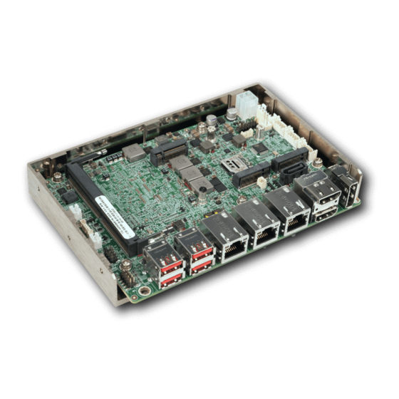
Page 12: Ntroduction
1.1 Introduction Figure 1-1: WAFER-TGL-U The WAFER-TGL-U series is a 3.5" form factor single bard computer. It has an on-board generation Intel® Core™ i7/i5/i3 or Celeron® processor, and supports one 260-pin 3200 MHz dual-channel DDR4 SDRAM SO-DIMM slot with up to 32.0 GB of memory. -
Page 13: Model Variations
WAFER-TGL-U SBC 1.2 Model Variations The model variations of the WAFER-TGL-U series are listed below. Model No. Intel® Core™ i7-1185G7E on-board SoC WAFER-TGL-U-i7 (1.8 GHz, quad-core, 12 MB cache, TDP=15 W) Intel® Core™ i5-1145G7E on-board SoC WAFER-TGL-U-i5 (1.5 GHz, quad-core, 8 MB cache, TDP=15 W) Intel®... -
Page 14: Connectors
WAFER-TGL-U SBC 1.4 Connectors The connectors on the WAFER-TGL-U are shown in the figure below. Figure 1-2: Connectors Page 4... -
Page 15: Dimensions
WAFER-TGL-U SBC 1.5 Dimensions The dimensions of the board are listed below: Figure 1-3: Dimensions (mm) Page 5... -
Page 16: Data Flow
WAFER-TGL-U SBC 1.6 Data Flow Figure 1-4 shows the data flow between the system chipset, the CPU and other components installed on the motherboard. Figure 1-4: Data Flow Diagram Page 6... -
Page 17: Technical Specifications
WAFER-TGL-U SBC 1.7 Technical Specifications WAFER-TGL-U technical specifications are listed below. Specification WAFER-TGL-U generation Intel ® mobile ULT on-board SoC: Core™ i7-1185G7E on-board SoC ® Intel (1.8 GHz, quad-core, 12 MB cache, TDP=15 W) Core™ i5-1145G7E on-board SoC ®... -
Page 18: Table 1-2: Technical Specifications
WAFER-TGL-U SBC I/O Interface Audio Connector 1 x iAUDIO (2x5 pin) supporting IEI AC-KIT-888S kit Ethernet 3 x RJ-45 2.5GbE port Serial Ports 1 x RS-232 by 10-pin (2x5) header 2 x RS-232/422/485 by 10-pin (2x5) header USB Ports 4 x USB 3.2 Gen 2 (10Gb/s) on rear I/O 2 x USB 2.0 by 8-pin (2x4) header... -
Page 19: Unpacking
WAFER-TGL-U SBC Chapter Unpacking Page 9... -
Page 20: Anti-Static Precautions
Only handle the edges of the PCB: Don't touch the surface of the motherboard. Hold the motherboard by the edges when handling. 2.2 Unpacking Precautions When the WAFER-TGL-U is unpacked, please do the following: Follow the antistatic guidelines above. -
Page 21: Packing List
If any of the components listed in the checklist below are missing, do not proceed with the installation. Contact the IEI reseller or vendor the WAFER-TGL-U was purchased from or contact an IEI sales representative directly by sending an email to sales@ieiworld.com. -
Page 22: Optional Items
WAFER-TGL-U SBC 2.4 Optional Items The following are optional components which may be separately purchased: Item and Part Number Image RS-232/422/485 cable, 250 mm, p=1.25 (P/N : 32205-002700-200-RS) Audio kit, 7.1 Channel (P/N: AC-KIT-888S) USB cable, 300mm, P=2.00 (P/N: CB-USB02A-RS) -
Page 23: Connectors
WAFER-TGL-U SBC Chapter Connectors Page 13... -
Page 24: Peripheral Interface Connectors
WAFER-TGL-U SBC 3.1 Peripheral Interface Connectors This chapter details all the jumpers and connectors. 3.1.1 WAFER-TGL-U Layout The figures below show all the connectors and jumpers. Figure 3-1: Connector and Jumper Locations 3.1.2 Peripheral Interface Connectors The table below lists all the connectors on the board. -
Page 25: External Interface Panel Connectors
WAFER-TGL-U SBC iDPM connector 75-pin slot IDPM M.2 2230 A-key slot M.2 A-key slot M2_AE1 M.2 3052/2042 B-key slot M.2 B-key slot M2_B1 Memory module slot 260-pin DDR4 SO-DIMM DIMM1 Power connector 4-pin Molex PWR1 Power button connector 2-pin wafer... -
Page 26: Internal Peripheral Connectors
WAFER-TGL-U SBC 3.2 Internal Peripheral Connectors The section describes all of the connectors on the WAFER-TGL-U. 3.2.1 Audio Connector CN Label: IAUDIO1 CN Type: 10-pin header, p=2.00 mm CN Location: See Figure 3-2 CN Pinouts: See Table 3-3 The audio connector can be connected with IEI AC-KIT-888S HD audio module to provide audio input and output to and from the system. -
Page 27: Battery Connector
Dispose of used batteries according to instructions and local regulations. NOTE: It is recommended to attach the RTC battery onto the system chassis in which the WAFER-TGL-U is installed. CN Label: BAT1 CN Type: 2-pin wafer, p=1.25 mm... -
Page 28: Digital I/O Connector
WAFER-TGL-U SBC Description VBAT+ Table 3-4: Battery Connector Pinouts 3.2.3 Digital I/O Connector CN Label: DIO1 CN Type: 14-pin header, p=2.00 mm CN Location: See Figure 3-4 CN Pinouts: See Table 3-5 The 12-bit digital I/O connector provides programmable input and output for external devices. -
Page 29: Fan Connector
WAFER-TGL-U SBC PIN NO. DESCRIPTION PIN NO. DESCRIPTION DOUT3 DOUT2 DOUT1 DOUT0 DIN5 DIN4 DIN3 DIN2 DIN1 DIN0 Table 3-5: Digital I/O Connector Pinouts 3.2.4 Fan Connector CN Label: CPU/FAN1 CN Type: 4-pin wafer, p=2.54 mm CN Location: See Figure 3-5... -
Page 30: Front Panel Connector
WAFER-TGL-U SBC 3.2.5 Front Panel Connector CN Label: F_PANEL1 CN Type: 6-pin wafer, p=2.00 mm CN Location: See Figure 3-6 CN Pinouts: See Table 3-7 The front panel connector connects to the power LED indicator and HDD LED indicator on the system front panel. -
Page 31: Lan Led Connectors
WAFER-TGL-U SBC 3.2.6 LAN LED Connectors CN Label: JLAN_LED2, JLAN_LED3 CN Type: 2-pin header, p=2.00 mm CN Location: See Figure 3-7 CN Pinouts: See Table 3-8 The LAN LED connectors connect to the LAN link LEDs on the system. Figure 3-7: LAN LED Connector Locations Description +3.3V... -
Page 32: Idpm Connector
WAFER-TGL-U SBC 3.2.7 iDPM Connector CN Label: IDPM CN Type: 75-pin slot, p=0.5 mm CN Location: See Figure 3-8 CN Pinouts: See Table 3-9 The iDPM slot only use for IEI eDP/LVDS/VGA module Figure 3-8: iDPM Connector Location Description Description +3.3V... -
Page 33: Table 3-9: Idpm Connector Pinouts
WAFER-TGL-U SBC Description Description Module Key +3.3VS DISPLAY_DETECT_P +3.3VS IN21 DISPLAY_DETECT_P +3.3VS IN23 +3.3VS EDP_TX3_DN +12VS EDP_TX3_DP +12VS +12VS EDP_TX2_DN +12VS EDP_TX2_DP SMB_CLK EDP_TX1_DN SMB_DATA EDP_TX1_DP EC_BKLT_CTRL EDP_TX0_DN EDP1_BKLT_CTRL EDP_TX0_DP EDP1_BKLT_EN EDP1_VDD_EN # EDP_AUX_DN EDP_HPD_R EDP_AUX_DP BUF_PLT_RST# LVDS_EN +V5S +V5S... -
Page 34: Slot, B-Key
WAFER-TGL-U SBC 3.2.8 M.2 Slot, B-key CN Label: M2_B1 CN Type: M.2 B-key slot CN Location: See Figure 3-9 CN Pinouts: See Table 3-10 Figure 3-9: M.2 B-key Slot Location The M.2 slot is keyed in the B position and accepts 3052/2242 size of M.2 modules. The M.2 slot supports PCIe x2 and USB 2.0 signals. -
Page 35: Table 3-10: M.2 B-Key Slot Pinouts
WAFER-TGL-U SBC Module Key Module Key Module Key Module Key Module Key CONFIG_0 PCIE_RXN5 WWAN_UIM_RST PCIE_RXP5 WWAN_UIM_CLK WWAN_UIM_DATA PCIE_TXN5 UIM_PWR PCIE_TXP5 DEVSLP PCIE_RXN4 PCIE_RXP4 PCIE_TXN4 PCIE_TXP4 BUF_PLT_RST# REFCLKN PCIE_WAKE# REFCLKP WWAN_RST +3.3V +3.3V +3.3V Table 3-10: M.2 B-Key Slot Pinouts... -
Page 36: Slot, A-Key
WAFER-TGL-U SBC 3.2.9 M.2 Slot, A-key CN Label: M2_A1 CN Type: M.2 A-key slot CN Location: See Figure 3-10 CN Pinouts: See Table 3-11 The M.2 slot is keyed in the A position and accepts 2230 size of M.2 modules. The M.2 slot supports PCIe x1 and USB 2.0 signals. -
Page 37: Table 3-11: M.2 A-Key Slot Pinouts
WAFER-TGL-U SBC Description Description PCIE_TX9+ PCIE_TX9- CL_RST# CL_DATA PCIE_RX9+ CL_CLK PCIE_RX9- CLK_M2_A+ CLK_M2_A- BUF_PLT_RST# Pull Up +V3.3A Pull Up +V3.3A +V3.3A +V3.3A Table 3-11: M.2 A-Key Slot Pinouts Page 27... -
Page 38: Ddr4 So-Dimm Socket
WAFER-TGL-U SBC 3.2.10 DDR4 SO-DIMM Socket CN Label: DIMM1 CN Type: 260-pin DDR4 SO-DIMM socket CN Location: Figure 3-11 791H The SO-DIMM slot is for installing the DDR4 SO-DIMM. Figure 3-11: DDR4 SO-DIMM Socket Location Page 28... -
Page 39: Power Connector
WAFER-TGL-U SBC 3.2.11 Power Connector CN Label: PWR1 CN Type: 4-pin Molex, p=4.2 mm CN Location: See Figure 3-12 CN Pinouts: See Table 3-12 The connector supports the +12V power supply. Figure 3-12: +12V DC-IN Power Connector Location PIN NO. -
Page 40: Power Button Connector
WAFER-TGL-U SBC 3.2.12 Power Button Connector CN Label: PWR_BTN1 CN Type: 2-pin wafer, p=2.00 mm CN Location: See Figure 3-13 CN Pinouts: See Table 3-13 The power button connector is connected to a power switch on the system chassis to enable users to turn the system on and off. -
Page 41: Reset Button Connector
WAFER-TGL-U SBC 3.2.13 Reset Button Connector CN Label: RST_BTN1 CN Type: 2-pin wafer, p=2.00 mm CN Location: See Figure 3-14 CN Pinouts: See Table 3-14 The reset button connector is connected to a reset switch on the system chassis to enable users to reboot the system when the system is turned on. -
Page 42: Rs-232 Serial Port Connector
WAFER-TGL-U SBC 3.2.14 RS-232 Serial Port Connector CN Label: COM1 CN Type: 10-pin header, p=2.0 mm CN Location: See Figure 3-15 CN Pinouts: See Table 3-15 The serial connector provides RS-232 connection. Figure 3-15: RS-232 Serial Port Connector Location PIN NO. -
Page 43: Rs-232/422/485 Serial Port Connector
WAFER-TGL-U SBC 3.2.15 RS-232/422/485 Serial Port Connector CN Label: COM2, COM3 CN Type: 10-pin header, p=2.0 mm CN Location: See Figure 3-16 CN Pinouts: See Table 3-16 This connector provides RS-232, RS-422 or RS-485 communications. The default mode is set to RS-232. Use BIOS to configure the connectors as RS-422 or RS-485. -
Page 44: Table 3-16: Rs-232/422/485 Serial Port Connector Pinouts
WAFER-TGL-U SBC RS-232 RS-422 RS-485 Table 3-16: RS-232/422/485 Serial Port Connector Pinouts Use the optional RS-232/422/485 cable to connect to a serial device. The pinouts of the DB-9 connector are listed below. RS-232 RS-422 RS-485 TXD422- TXD485- TXD422+ TXD485+ RXD422+... -
Page 45: Sata 6Gb/S Drive Connector
WAFER-TGL-U SBC 3.2.16 SATA 6Gb/s Drive Connector CN Label: SATA1 CN Type: 7-pin SATA connector CN Location: See Figure 3-17 The SATA 6Gb/s drive connector is connected to a SATA 6Gb/s drive. The SATA 6Gb/s drive transfers data at speeds as high as 6Gb/s. -
Page 46: Sata Power Connector
WAFER-TGL-U SBC 3.2.17 SATA Power Connector CN Label: SATA_PWR1 CN Type: 2-pin wafer, p=2.00 mm CN Location: See Figure 3-18 CN Pinouts: See Table 3-18 The SATA power connector provides +5 V power output to the SATA connector. Figure 3-18: SATA Power Connector Location... -
Page 47: Smbus/I C Connector
WAFER-TGL-U SBC 3.2.18 SMBus/I C Connector CN Label: I2C1 CN Type: 4-pin wafer, p=1.25 mm CN Location: See Figure 3-19 CN Pinouts: See Table 3-19 The SMBus (System Management Bus) connector provides low-speed system management communications. Figure 3-19: SMBus Connector Location... -
Page 48: Usb 2.0 Connector
WAFER-TGL-U SBC 3.2.19 USB 2.0 Connector CN Label: USB2_CN1 CN Type: 8-pin header, p=2.00 mm CN Location: See Figure 3-20 CN Pinouts: See Table 3-20 The USB connector provides two USB 2.0 ports by dual-port USB cable. Figure 3-20: USB Connector Location PIN NO. -
Page 49: External Peripheral Interface Connector Panel
WAFER-TGL-U SBC 3.3 External Peripheral Interface Connector Panel Figure 3-21 shows the WAFER-TGL-U external peripheral interface connector (EPIC) panel. The EPIC panel consists of the following: 2 x HDMI connector 1 x DP connector 3 x 2.5GbE RJ-45 connector ... -
Page 50: Hdmi Connectors
WAFER-TGL-U SBC 3.3.1 HDMI Connectors CN Label: HDMI1 CN Type: HDMI connector CN Location: See Figure 3-21 CN Pinouts: See Table 3-21 and Figure 3-22 The HDMI connectors can connect to HDMI devices. Description Description HDMI_DATA2 HDMI_DATA2# HDMI_DATA1 HDMI_DATA1# HDMI_DATA0... -
Page 51: Dp Connector
WAFER-TGL-U SBC 3.3.2 DP Connector CN Label: CN Type: DP connector CN Location: See Figure 3-21 CN Pinouts: See Table 3-22 and Figure 3-23 The DP connectors can connect to DP devices. PIN NO. DESCRIPTION PIN NO. DESCRIPTION DATA_0P DATA_3N... -
Page 52: Lan Connectors
WAFER-TGL-U SBC 3.3.3 LAN Connectors CN Label: LAN1, LAN2, LAN3 CN Type: RJ-45 CN Location: Figure 3-21 808H CN Pinouts: Figure 3-24 and Table 3-23 809H The LAN connector connects to a local network. Description Description MDIA0+ MDIA2+ MDIA0- MDIA1-... -
Page 53: Usb 3.2 Gen 2 Connectors
Table 3-25 and Figure 3-25 815H The WAFER-TGL-U has four external USB 3.2 Gen 2 ports. The USB connector can be connected to a USB 2.0 or USB 3.2 device. The pinouts of USB 3.2 Gen 2 connectors are shown below. -
Page 54: Installation
WAFER-TGL-U SBC Chapter Installation Page 44... -
Page 55: Anti-Static Precautions
WAFER-TGL-U and severe injury to the user. Electrostatic discharge (ESD) can cause serious damage to electronic components, including the WAFER-TGL-U. Dry climates are especially susceptible to ESD. It is therefore critical that whenever the WAFER-TGL-U or any other electrical component is handled, the following anti-static precautions are strictly adhered to. - Page 56 Turn all power to the WAFER-TGL-U off: When working with the WAFER-TGL-U, make sure that it is disconnected from all power supplies and that no electricity is being fed into the system. Before and during the installation of the WAFER-TGL-U DO NOT: ...
-
Page 57: So-Dimm Installation
WAFER-TGL-U SBC 4.3 SO-DIMM Installation To install an SO-DIMM, please follow the steps below and refer to Figure 4-1. Figure 4-1: SO-DIMM Installation Step 1: Locate the SO-DIMM socket. Place the board on an anti-static mat. Step 2: Align the SO-DIMM with the socket. Align the notch on the memory with the notch on the memory socket. -
Page 58: Module Installation
WAFER-TGL-U SBC 4.4 M.2 Module Installation To install an M.2 module, please follow the steps below. Step 1: Locate the M.2 module slot. See Chapter 3. Step 2: Remove the retention screw secured on the motherboard. Step 3: Line up the notch on the module with the notch on the slot. Slide the M.2 module into the socket at an angle of about 20º... -
Page 59: System Configuration
CN Location: See Figure 4-5 If the WAFER-TGL-U fails to boot due to improper BIOS settings, use the button to clear the CMOS data and reset the system BIOS information. The location of the clear CMOS button is shown in Figure 4-5... -
Page 60: Flash Descriptor Security Override Jumper
WAFER-TGL-U SBC 4.5.3 Flash Descriptor Security Override Jumper CN Label: ME_FLASH1 CN Type: 2-pin header, p=1.27 mm CN Location: See Figure 4-6 CN Settings: See Table 4-1 The Flash Descriptor Security Override jumper (ME_FLASH1) allows to enable or disable the ME firmware update. Refer to Figure 4-6 and Table 4-1 for the jumper location and settings. -
Page 61: Chassis Installation
WAFER-TGL-U without the heat spreader secured to the board. When the WAFER-TGL-U is shipped, it is secured to a heat spreader with five retention screws. The heat spreader must have a direct contact with a heat dissipation surface to ensure stable operation. -
Page 62: Figure 4-7: Heat Sink Retention Screws
WAFER-TGL-U SBC If the WAFER-TGL-U must be removed from the heat spreader, the four retention screws must be removed. Figure 4-7: Heat Sink Retention Screws Page 52... -
Page 63: Motherboard Installation Example
WAFER-TGL-U SBC 4.6.2 Motherboard Installation Example Each side of the heat spreader has several screw holes allowing the WAFER-TGL-U to be mounted into a chassis or a heat sink enclosure (please refer to Figure 1-3 for the detailed dimensions). The user has to design or select a chassis or a heat sink enclosure that has screw holes matching up with the holes on the heat spreader for installing the WAFER-TGL-U. -
Page 64: Figure 4-9: Power Cable To Motherboard Connection
WAFER-TGL-U SBC Step 2: Connect the power cable to the motherboard. Connect the 4-pin (2x2) Molex type power cable connector to the power connector on the motherboard. See Figure 4-9. Figure 4-9: Power Cable to Motherboard Connection Step 3: Connect power cable to power supply. Connect one of the 4-pin (1x4) Molex type power cable connectors to an AT power supply. -
Page 65: Channel Audio Kit Installation
WAFER-TGL-U SBC Figure 4-10: Connect Power Cable to Power Supply 4.7.2 7.1 Channel Audio Kit Installation NOTE: This item must be ordered separately, and connects to the audio connector. For further information please contact the nearest distributor, reseller or vendor or contact an IEI sales representative directly. -
Page 66: Rs-232 Cable Connection
WAFER-TGL-U SBC Figure 4-11: 7.1 Channel Audio Kit Step 3: Mount the audio kit onto the chassis. Once the audio kit is connected to the board, secure the audio kit bracket to the system chassis. Step 4: Connect the audio devices. Connect speakers and external audio sources to the audio jacks on the audio kit. -
Page 67: Sata Drive Connection
Step 0: system. 4.7.4 SATA Drive Connection The WAFER-TGL-U is shipped with a SATA drive cable. To connect the SATA drive to the connector, please follow the steps below. Step 1: Locate the SATA connector and the SATA power connector. The locations of the connectors are shown in Chapter 3. -
Page 68: Figure 4-13: Sata Drive Cable Connection
WAFER-TGL-U SBC Figure 4-13: SATA Drive Cable Connection Step 3: Connect the cable to the SATA disk. Connect the connector on the other end of the cable to the connector at the back of the SATA drive. See Figure 4-13. -
Page 69: Software Drivers
WAFER-TGL-U SBC Chapter Software Drivers Page 59... -
Page 70: Available Drivers
WAFER-TGL-U SBC 5.1 Available Drivers All the drivers for the WAFER-TGL-U are available on IEI Resource Download Center (https://download.ieiworld.com). Type WAFER-TGL-U and press Enter to find all the relevant software, utilities, and documentation. Figure 5-1: IEI Resource Download Center 5.2 Driver Download To download drivers from IEI Resource Download Center, follow the steps below. - Page 71 WAFER-TGL-U SBC Step 3: Click the driver file name on the page and you will be prompted with the following window. You can download the entire ISO file ( ), or click the small arrow to find an individual driver and click the file name to download (...
-
Page 72: A Regulatory Compliance
WAFER-TGL-U SBC Appendix Regulatory Compliance Page 62... - Page 73 WAFER-TGL-U SBC DECLARATION OF CONFORMITY This equipment has been tested and found to comply with specifications for CE marking. If the user modifies and/or installs other devices in the equipment, the CE conformity declaration may no longer apply. FCC WARNING This equipment complies with Part 15 of the FCC Rules.
-
Page 74: B Product Disposal
WAFER-TGL-U SBC Appendix Product Disposal Page 64... - Page 75 WAFER-TGL-U SBC CAUTION: Risk of explosion if battery is replaced by an incorrect type. Only certified engineers should replace the on-board battery. Dispose of used batteries according to instructions and local regulations. Outside the European Union–If you wish to dispose of used electrical and electronic products outside the European Union, please contact your local authority so as to comply with the correct disposal method.
-
Page 76: C Digital I/O Interface
WAFER-TGL-U SBC Appendix Digital I/O Interface Page 66... - Page 77 WAFER-TGL-U SBC The DIO connector on the WAFER-TGL-U is interfaced to GPIO ports on the Super I/O chipset. The digital inputs and digital outputs are generally control signals that control the on/off circuit of external devices or TTL devices. Data can be read or written to the selected address to enable the DIO functions.
- Page 78 WAFER-TGL-U SBC AH – 6FH Sub-function: AL – 9 :Set the digital port as OUTPUT :Digital I/O output value Assembly Language Sample 2 AX, 6F09H ;setting the digital port as output BL, 09H ;digital value is 09H Digital Output is 1001b...
-
Page 79: D Watchdog Timer
WAFER-TGL-U SBC Appendix Watchdog Timer Page 69... - Page 80 WAFER-TGL-U SBC NOTE: The following discussion applies to DOS. Contact IEI support or visit the IEI website for drivers for other operating systems. The Watchdog Timer is a hardware-based timer that attempts to restart the system when it stops working. The system may stop working because of external EMI or software bugs.
- Page 81 WAFER-TGL-U SBC NOTE: The Watchdog Timer is activated through software. The software application that activates the Watchdog Timer must also deactivate it when closed. If the Watchdog Timer is not deactivated, the system will automatically restart after the Timer has finished its countdown.
-
Page 82: E Error Beep Code
WAFER-TGL-U SBC Appendix Error Beep Code Page 72... -
Page 83: Pei Beep Codes
WAFER-TGL-U SBC E.1 PEI Beep Codes Number of Beeps Description Memory not Installed Memory was installed twice (InstallPeiMemory routine in PEI Core called twice) Recovery started DXEIPL was not found DXE Core Firmware Volume was not found Recovery failed S3 Resume failed Reset PPI is not available E.2 DXE Beep Codes... -
Page 84: F Hazardous Materials Disclosure
WAFER-TGL-U SBC Appendix Hazardous Materials Disclosure Page 74... -
Page 85: Rohs Ii Directive (2015/863/Eu)
WAFER-TGL-U SBC F.1 RoHS II Directive (2015/863/EU) The details provided in this appendix are to ensure that the product is compliant with the RoHS II Directive (2015/863/EU). The table below acknowledges the presences of small quantities of certain substances in the product, and is applicable to RoHS II Directive (2015/863/EU). -
Page 86: China Rohs
WAFER-TGL-U SBC F.2 China RoHS 此附件旨在确保本产品符合中国 RoHS 标准。以下表格标示此产品中某有毒物质的含量符 合中国 RoHS 标准规定的限量要求。 本产品上会附有”环境友好使用期限”的标签,此期限是估算这些物质”不会有泄漏或突变”的 年限。本产品可能包含有较短的环境友好使用期限的可替换元件,像是电池或灯管,这些元 件将会单独标示出来。 部件名称 有毒有害物质或元素 壳体 印刷电路板 金属螺帽 电缆组装 风扇组装 电力供应组装 电池 O: 表示该有毒有害物质在该部件所有物质材料中的含量均在 SJ/T11364-2014 與 GB/T26572-2011 标准规定的限量要求以下。 X: 表示该有毒有害物质至少在该部件的某一均质材料中的含量超出 SJ/T11364-2014 與 GB/T26572-2011 标准规定的限量要求。 Page 76...
Need help?
Do you have a question about the WAFER-TGL-U and is the answer not in the manual?
Questions and answers