Table of Contents
Advertisement
Quick Links
Advertisement
Table of Contents

Related Manuals for IEI Technology WAFER-ULT4


Summary of Contents for IEI Technology WAFER-ULT4
- Page 1 WAFER-ULT3/ULT4 3.5" SBC MODEL: WAFER-ULT3/ULT4 3.5” SBC with 6 Generation Intel® Mobile Core™ i7/i5/i3 or Celeron® SoC, DDR4 SO-DIMM, Triple Display, Dual GbE, PCIe Mini, SATA 6Gb/s, USB 3.1 Gen1, COM and RoHS User Manual Page i Rev. 1.04 – June 18, 2019...
- Page 2 WAFER-ULT3/ULT4 3.5" SBC Revision Date Version Changes June 18, 2019 1.04 Clarified the LVDS connector pinouts (Section 3.2.9) February 27, 2019 1.03 Corrected Table 4-4: LVDS Voltage Selection Jumper Settings October 30, 2018 1.02 Modified Section 4.7: Motherboard Installation Modified the part number of the optional RS-232/422/485 cable.
- Page 3 WAFER-ULT3/ULT4 3.5" SBC Copyright COPYRIGHT NOTICE The information in this document is subject to change without prior notice in order to improve reliability, design and function and does not represent a commitment on the part of the manufacturer. In no event will the manufacturer be liable for direct, indirect, special, incidental, or consequential damages arising out of the use or inability to use the product or documentation, even if advised of the possibility of such damages.
- Page 4 WAFER-ULT3/ULT4 3.5" SBC Manual Conventions WARNING Warnings appear where overlooked details may cause damage to the equipment or result in personal injury. Warnings should be taken seriously. CAUTION Cautionary messages should be heeded to help reduce the chance of losing data or damaging the product. NOTE These messages inform the reader of essential but non-critical information.
-
Page 5: Table Of Contents
WAFER-ULT3/ULT4 3.5" SBC Table of Contents 1 INTRODUCTION ......................1 1.1 I ......................2 NTRODUCTION 1.2 M ....................3 ODEL ARIATIONS 1.3 F ........................3 EATURES 1.4 C ......................4 ONNECTORS 1.5 D ....................... 6 IMENSIONS 1.6 D ........................ 8 1.7 T .................. - Page 6 WAFER-ULT3/ULT4 3.5" SBC 3.2.10 PCIe Mini Card Slot (with mSAT Support) ............ 28 3.2.11 PCIe Mini Card Slot (with SIM Card Socket) ..........30 3.2.12 Power and HDD LED Connector ..............32 3.2.13 Power Button Connector ................33 3.2.14 Reset Button Connector ................. 34 3.2.15 RS-232/422/485 Serial Port Connectors ............
- Page 7 WAFER-ULT3/ULT4 3.5" SBC 4.8 I ............62 NTERNAL ERIPHERAL EVICE ONNECTIONS 4.8.1 AT/ATX Power Connection ................62 4.8.2 SATA Drive Connection ................... 64 4.9 A USB 3.1 G DDING RIVERS TO A INDOWS NSTALLATION MAGE ® M ULT O ) ......... 65 ENERATION NTEL OBILE...
- Page 8 WAFER-ULT3/ULT4 3.5" SBC 5.4.2 PCH-IO Configuration ..................96 5.4.2.1 PCI Express Configuration ............... 97 5.4.2.2 SATA Configuration .................. 99 5.4.2.3 HD Audio Configuration ................. 100 5.5 S ....................... 101 ECURITY 5.6 B ........................102 5.7 S & E ......................104 A REGULATORY COMPLIANCE ................
- Page 9 WAFER-ULT3/ULT4 3.5" SBC List of Figures Figure 1-1: WAFER-ULT3/ULT4 ..................... 2 Figure 1-2: Connectors (Front Side) ..................... 4 Figure 1-3: Connectors (Solder Side) ................... 5 Figure 1-4: WAFER-ULT3/ULT4 Dimensions (mm) ..............6 Figure 1-5: Dimensions with Optional Heatsink (mm) ..............7 Figure 1-6: Data Flow Diagram ......................
- Page 10 WAFER-ULT3/ULT4 3.5" SBC Figure 3-25: HDMI Connector Pinout Locations ................ 43 Figure 3-26: USB 3.1 Gen 1 Port Pinout Locations ..............44 Figure 3-27: VGA Connector ....................... 45 Figure 4-1: SO-DIMM Installation ....................49 Figure 4-2: Removing the Retention Screw ................50 Figure 4-3: Inserting the PCIe Mini Card into the Slot at an Angle ..........
- Page 11 WAFER-ULT3/ULT4 3.5" SBC List of Tables Table 1-1: Model Variations ......................3 Table 1-2: WAFER-ULT3/ULT4 Specifications ................10 Table 2-1: Packing List ......................... 13 Table 2-2: Optional Items ......................14 Table 3-1: Peripheral Interface Connectors ................17 Table 3-2: External Peripheral Connectors ................18 Table 3-3: Power Connector Pinouts ..................
- Page 12 WAFER-ULT3/ULT4 3.5" SBC Table 4-1: AT/ATX Power Mode Switch Settings ............... 53 Table 4-2: Flash Descriptor Security Override Jumper Settings ..........54 Table 4-3: LVDS Panel Type Selection ..................56 Table 4-4: LVDS Voltage Selection Jumper Settings ..............57 Table 4-5: Signal Mode Settings for Serial Port 1 ..............58 Table 4-6: Signal Mode Settings for Serial Port 2 ..............
- Page 13 WAFER-ULT3/ULT4 3.5" SBC BIOS Menus BIOS Menu 1: Main ........................73 BIOS Menu 2: Advanced ......................74 BIOS Menu 3: CPU Configuration ....................75 BIOS Menu 4: PCH-FW Configuration ..................77 BIOS Menu 5: ACPI Settings ....................... 78 BIOS Menu 6: F81866 Super IO Configuration ................79 BIOS Menu 7: Serial Port n Configuration Menu ...............
-
Page 15: Introduction
WAFER-ULT3/ULT4 3.5" SBC Chapter Introduction Page 1... -
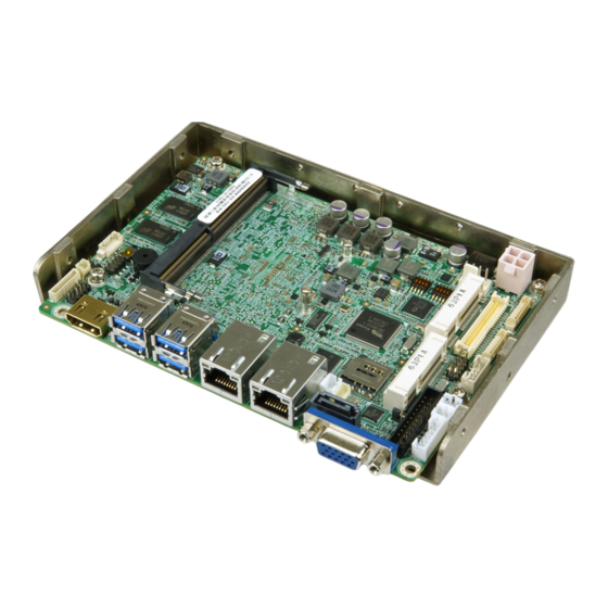
Page 16: Ntroduction
WAFER-ULT3/ULT4 3.5" SBC 1.1 Introduction Figure 1-1: WAFER-ULT3/ULT4 The WAFER-ULT3/ULT4 3.5” SBC is a 6 generation Intel® mobile ULT SoC platform that supports one 2133 MHz DDR4 SO-DIMM and on-board memory (optional, by request). The WAFER-ULT3/ULT4 provides two GbE interfaces through the Intel® I219LM (with Intel®... -
Page 17: Model Variations
The model variations of the WAFER-ULT3/ULT4 are listed below. Model On-board SoC 7th Generation Intel® Mobile ULT On-board SoC WAFER-ULT4-i7 Intel® Core™ i7-7600U (up to 3.9 GHz, dual-core, 4 MB cache, TDP=15W) (MOQ: 100 pcs/lot) WAFER-ULT4-i5 Intel® Core™ i5-7300U (up to 3.5 GHz, dual-core, 3 MB cache, TDP=15W) WAFER-ULT4-i3 Intel®... -
Page 18: Connectors
WAFER-ULT3/ULT4 3.5" SBC 1.4 Connectors The connectors on the WAFER-ULT3/ULT4 are shown in the figure below. Figure 1-2: Connectors (Front Side) Page 4... -
Page 19: Figure 1-3: Connectors (Solder Side)
WAFER-ULT3/ULT4 3.5" SBC Figure 1-3: Connectors (Solder Side) Page 5... -
Page 20: Dimensions
WAFER-ULT3/ULT4 3.5" SBC 1.5 Dimensions The main dimensions of the WAFER-ULT3/ULT4 are shown in the diagram below. Figure 1-4: WAFER-ULT3/ULT4 Dimensions (mm) Page 6... -
Page 21: Figure 1-5: Dimensions With Optional Heatsink (Mm)
WAFER-ULT3/ULT4 3.5" SBC Figure 1-5 shows the dimensions of the WAFER-ULT3/ULT4 installed with the optional heatsink (P/N: 34000-000673-RS). Figure 1-5: Dimensions with Optional Heatsink (mm) Page 7... -
Page 22: Data Flow
WAFER-ULT3/ULT4 3.5" SBC 1.6 Data Flow Figure 1-6 shows the data flow between the system chipset, the CPU and other components installed on the motherboard. Figure 1-6: Data Flow Diagram Page 8... -
Page 23: Technical Specifications
WAFER-ULT3/ULT4 3.5" SBC 1.7 Technical Specifications The WAFER-ULT3/ULT4 technical specifications are listed below. Specifications WAFER-ULT3/ULT4 Form Factor 3.5” 7th generation Intel® mobile ULT on-board SoC: Intel® Core™ i7-7600U (up to 3.9 GHz, dual-core, 4 MB cache, TDP=15W) Intel® Core™ i5-7300U (up to 3.5 GHz, dual-core, 3 MB cache, TDP=15W) Intel®... -
Page 24: Table 1-2: Wafer-Ult3/Ult4 Specifications
WAFER-ULT3/ULT4 3.5" SBC Specifications WAFER-ULT3/ULT4 One full-size PCIe Mini card slot (with SATA signal, supports mSATA) One full-size PCIe Mini card slot (with SIM card socket) Expansions *3855U SoC belongs to Skylake ULT Base series which supports PCIe Gen 2 signal only. One audio connector (10-pin header, supports 7.1-channel HD audio by Audio IEI AC-KIT-892HD kit) -
Page 25: Packing List
WAFER-ULT3/ULT4 3.5" SBC Chapter Packing List Page 11... -
Page 26: Anti-Static Precautions
WAFER-ULT3/ULT4 3.5" SBC 2.1 Anti-static Precautions WARNING! Static electricity can destroy certain electronics. Make sure to follow the ESD precautions to prevent damage to the product, and injury to the user. Make sure to adhere to the following guidelines: Wear an anti-static wristband: Wearing an anti-static wristband can prevent ... -
Page 27: Packing List
WAFER-ULT3/ULT4 3.5" SBC 2.3 Packing List NOTE: If any of the components listed in the checklist below are missing, do not proceed with the installation. Contact the IEI reseller or vendor the WAFER-ULT3/ULT4 was purchased from or contact an IEI sales representative directly by sending an email to sales@ieiworld.com. -
Page 28: Optional Items
WAFER-ULT3/ULT4 3.5" SBC 2.4 Optional Items These optional items are available. Item and Part Number Image RS-232/422/485 cable (250 mm, P=1.25) (P/N: 32005-003500-200-RS) Dual-port USB 2.0 cable, 210 mm, p=2.00 mm (P/N: 32001-008600-200-RS) Heatsink for WAFER-ULT3/ULT4, 146 mm x 102 mm x 14.6 mm (P/N: 34000-000673-RS) Table 2-2: Optional Items... -
Page 29: Connectors
WAFER-ULT3/ULT4 3.5" SBC Chapter Connectors Page 15... -
Page 30: Peripheral Interface Connectors
WAFER-ULT3/ULT4 3.5" SBC 3.1 Peripheral Interface Connectors This chapter details all the peripheral interface connectors. 3.1.1 WAFER-ULT3/ULT4 Layout The figure below shows all the peripheral interface connectors. Figure 3-1: Peripheral Interface Connectors Page 16... -
Page 31: Peripheral Interface Connectors
WAFER-ULT3/ULT4 3.5" SBC 3.1.2 Peripheral Interface Connectors The table below lists all the connectors on the board. Connector Type Label 4-pin Molex power +12V power connector PWR1 connector 5 V SATA power connector 2-pin wafer SATA_PWR1 Audio connector 10-pin header J_AUDIO1 Battery connector 2-pin wafer... -
Page 32: External Interface Panel Connectors
WAFER-ULT3/ULT4 3.5" SBC 3.1.3 External Interface Panel Connectors The table below lists the connectors on the external I/O panel. Connector Type Label GbE connectors RJ-45 LAN1, LAN2 HDMI connector HDMI HDMI1 Dual USB 3.1 Gen 1 USB_CON1, USB 3.1 Gen 1 connectors port USB_CON2 VGA connector... -
Page 33: Figure 3-2: Power Connector Location
WAFER-ULT3/ULT4 3.5" SBC Figure 3-2: Power Connector Location Description Description +12V +12V Table 3-3: Power Connector Pinouts Page 19... -
Page 34: Sata Power Connector
WAFER-ULT3/ULT4 3.5" SBC 3.2.2 5 V SATA Power Connector CN Label: SATA_PWR1 CN Type: 2-pin wafer, p=2 mm CN Location: See Figure 3-3 CN Pinouts: See Table 3-4 Use the 5 V SATA power connector to connect to SATA device power connection. Figure 3-3: 5 V SATA Power Connector Location Description Table 3-4: 5 V SATA Power Connector Pinouts... -
Page 35: Battery Connector
WAFER-ULT3/ULT4 3.5" SBC The audio connector is connected to external audio devices including speakers and microphones for the input and output of audio signals to and from the system. Figure 3-4: Audio Connector Location Description Description HDA_SYNC HDA_CLK HDA_SDO HDA_BEEP HDA_SDI HDA_RESET AUD_GND... -
Page 36: Figure 3-5: Battery Connector Location
WAFER-ULT3/ULT4 3.5" SBC NOTE: It is recommended to attach the RTC battery onto the system chassis in which the WAFER-ULT3/ULT4 is installed. CN Label: BAT1 CN Type: 2-pin wafer, p=1.25 mm CN Location: See Figure 3-5 CN Pinouts: See Table 3-6 This is connected to the system battery. -
Page 37: Cpu Fan Connector
WAFER-ULT3/ULT4 3.5" SBC 3.2.5 CPU Fan Connector CN Label: CPU/FAN1 CN Type: 4-pin wafer, p=2.54 mm CN Location: See Figure 3-6 CN Pinouts: See Table 3-7 The fan connector attaches to a system cooling fan. Figure 3-6: CPU Fan Connector Location Description +12V Rotation signal... -
Page 38: Digital I/O Connector
WAFER-ULT3/ULT4 3.5" SBC 3.2.6 Digital I/O Connector CN Label: DIO1 CN Type: 10-pin header, p=2 mm CN Location: See Figure 3-7 CN Pinouts: See Table 3-8 The digital I/O connector provides programmable input and output for external devices. The digital I/O provides 4-bit output and 4-bit input. Figure 3-7: Digital I/O Connector Location Description Description... -
Page 39: Internal Displayport Connector
WAFER-ULT3/ULT4 3.5" SBC 3.2.7 Internal DisplayPort Connector NOTE: The user can select either to use the VGA connector or the internal DisplayPort connector. Use the VGA/iDP selection switch to configure the settings. Please refer to Section 4.6.7 for detailed information. CN Label: CN Type: 20-pin box header, p=2 mm... -
Page 40: Lvds Backlight Control Connector
WAFER-ULT3/ULT4 3.5" SBC Description Description AUX_P AUX_N LANE2P LANE3P LANE2N LANE3N LANE0P LANE1P LANE0N LANE1N VCC3V VCC5V Table 3-9: Internal DisplayPort Connector Pinouts 3.2.8 LVDS Backlight Control Connector CN Label: INV1 CN Type: 5-pin wafer, p=2 mm CN Location: See Figure 3-9 CN Pinouts: See Table 3-10 The backlight control connector provides the backlight on the LCD display connected to... -
Page 41: Lvds Connector
WAFER-ULT3/ULT4 3.5" SBC Description LCD_BKLTCTL GROUND +12V GROUND BACKLIGHT ENABLE Table 3-10: LVDS Backlight Control Connector Pinouts 3.2.9 LVDS Connector CN Label: LVDS1 40-pin crimp, p=1.25 mm CN Type: CN Location: See Figure 3-10 CN Pinouts: See Table 3-11 The LVDS LCD connector can be connected to an 18/24-bit dual-channel LVDS panel. Figure 3-10: LVDS Connector Location NOTE: To use LVDS, the #33 pin of LVDS1 connector must be connected with... -
Page 42: Pcie Mini Card Slot (With Msat Support)
WAFER-ULT3/ULT4 3.5" SBC Description Description A_Y0# A_Y1# A_Y0 A_Y1 A_Y2# A_CK# A_Y2 A_CK A_Y3# B_Y0# A_Y3 B_Y0 B_Y1# B_Y2# B_Y1 B_Y2 B_CK# B_Y3# B_CK B_Y3 LVDS Detect (GND)* LVDS_VCC LVDS_VCC LVDS_VCC LVDS_VCC LVDS_VCC LVDS_VCC *LVDS Detect must be connected to GND. Table 3-11: LVDS Connector Pinouts 3.2.10 PCIe Mini Card Slot (with mSAT Support) CN Label:... -
Page 43: Figure 3-11: Pcie Mini Card Slot (With Msata Support) Location
WAFER-ULT3/ULT4 3.5" SBC Figure 3-11: PCIe Mini Card Slot (with mSATA Support) Location Description Description PCIE_WAKE# VCC3 1.5V PCIE_CLK# PCIE_CLK PCIRST# PCIE_RXN(SATA_RX+) PCIE_RXP(SATA_RX-) 1.5V SMBCLK PCIE_TXN(SATA_TX-) SMBDATA PCIE_TXP(SATA_TX+) Page 29... -
Page 44: Pcie Mini Card Slot (With Sim Card Socket)
WAFER-ULT3/ULT4 3.5" SBC Description Description USBD- USBD+ VCC3 VCC3 1.5V VCC3 Table 3-12: PCIe Mini Card Slot (with mSATA Support) Pinouts 3.2.11 PCIe Mini Card Slot (with SIM Card Socket) CN Label: MINI_PCIE1 CN Type: PCIe Mini card slot CN Location: See Figure 3-12 CN Pinouts: See Table 3-13... -
Page 45: Figure 3-12: Pcie Mini Card Slot (With Sim Card Socket) Location
WAFER-ULT3/ULT4 3.5" SBC Figure 3-12: PCIe Mini Card Slot (with SIM Card Socket) Location Description Description PCIE_WAKE# VCC3 1.5V UIM_PWR UIM_DATA PCIE_CLK# UIM_CLK PCIE_CLK UIM_RST UIM_VPP PCIRST# PCIE_RXN PCIE_RXP 1.5V SMBCLK PCIE_TXN SMBDATA Page 31... -
Page 46: Power And Hdd Led Connector
WAFER-ULT3/ULT4 3.5" SBC Description Description PCIE_TXP USBD- USBD+ VCC3 VCC3 1.5V M-SATA Detect VCC3 Table 3-13: PCIe Mini Card Slot (with SIM Card Socket) Pinouts 3.2.12 Power and HDD LED Connector CN Label: F_PANEL1 CN Type: 6-pin wafer, p=2 mm CN Location: See Figure 3-13 CN Pinouts:... -
Page 47: Power Button Connector
WAFER-ULT3/ULT4 3.5" SBC Function Description PWR_LED+ Power LED PWR_LED- HDD_LED+ HDD LED HDD_LED- Table 3-14: Power and HDD LED Connector Pinouts 3.2.13 Power Button Connector CN Label: PWR_BTN1 CN Type: 2-pin wafer, p=2 mm See Figure 3-14 CN Location: CN Pinouts: See Table 3-15 The power button connector is connected to a power switch on the system chassis to enable users to turn the system on and off. -
Page 48: Reset Button Connector
WAFER-ULT3/ULT4 3.5" SBC 3.2.14 Reset Button Connector CN Label: RST_BTN1 CN Type: 2-pin wafer, p=2 mm CN Location: See Figure 3-15 CN Pinouts: See Table 3-16 The reset button connector is connected to a reset switch on the system chassis to enable users to reboot the system when the system is turned on. -
Page 49: Figure 3-16: Rs-232 Serial Port Connector Locations
WAFER-ULT3/ULT4 3.5" SBC These two connectors provide RS-232, RS-422 or RS-485 communications. The default mode is set to RS-232. To configure the connectors as RS-422 or RS-485, please refer to Section 4.6.6. Figure 3-16: RS-232 Serial Port Connector Locations RS-232 RS-422 RS-485 TXD-... -
Page 50: Sata 6Gb/S Connector
WAFER-ULT3/ULT4 3.5" SBC RS-232 RS-422 RS-485 TXD422- TXD485- TXD422+ TXD485+ RXD422+ RXD422- Table 3-18: DB-9 RS-232/422/485 Pinouts 3.2.16 SATA 6Gb/s Connector CN Label: SATA1 CN Type: 7-pin SATA drive connector CN Location: See Figure 3-17 CN Pinouts: See Table 3-19 The SATA drive connector can be connected to the SATA drive and supports up to 6Gb/s data transfer rate. -
Page 51: Sim Card Slot
WAFER-ULT3/ULT4 3.5" SBC Description Table 3-19: SATA 6Gb/s Drive Connector Pinouts 3.2.17 SIM Card Slot CN Label: SIM1 CN Type: SIM card slot CN Location: See Figure 3-18 NOTE: The SIM card slot accepts a SIM card for WWAN network communication. WWAN module must be installed in the MINI-PICE1 PCIe Mini slot to provide WWAN communication. -
Page 52: Smbus Connector
WAFER-ULT3/ULT4 3.5" SBC 3.2.18 SMBus Connector CN Label: SMB1 CN Type: 4-pin wafer, p=1.25 mm CN Location: See Figure 3-19 CN Pinouts: See Table 3-20 The SMBus (System Management Bus) connector provides low-speed system management communications. Figure 3-19: SMBus Connector Location Description SMBUS(I2C) DATA SMBUS(I2C) CLK... -
Page 53: So-Dimm Slot
WAFER-ULT3/ULT4 3.5" SBC 3.2.19 SO-DIMM Slot CN Label: DIMM2 CN Type: 260-pin DDR4 SO-DIMM slot CN Location: See Figure 3-20 The SO-DIMM slot is for installing the SO-DIMM on the system. Figure 3-20: SO-DIMM Slot Location Page 39... -
Page 54: Spi Flash Connector
WAFER-ULT3/ULT4 3.5" SBC 3.2.20 SPI Flash Connector CN Label: JSPI1 CN Type: 6-pin wafer, p=1.25 mm CN Location: See Figure 3-21 CN Pinouts: See Table 3-21 The SPI flash connector is used to flash the SPI ROM. Figure 3-21: SPI Flash Connector Location Description +3.3V_SPI_CON SPI_CS#0_N... -
Page 55: Usb 2.0 Connector
WAFER-ULT3/ULT4 3.5" SBC 3.2.21 USB 2.0 Connector CN Label: USB1 CN Type: 8-pin header, p=2 mm CN Location: See Figure 3-22 CN Pinouts: See Table 3-22 The USB header can connect to two USB 2.0/1.1 devices. Figure 3-22: USB 2.0 Connector Location Description Description USB_VCC... -
Page 56: External Interface Connectors
WAFER-ULT3/ULT4 3.5" SBC 3.3 External Interface Connectors The figure below shows the external peripheral interface connector (EPIC) panel. The EPIC panel consists of the following: Figure 3-23: External Interface Connectors 3.3.1 GbE Connectors CN Label: LAN1, LAN2 CN Type: RJ-45 CN Location: See Figure 3-23 CN Pinouts:... -
Page 57: Hdmi Connector
WAFER-ULT3/ULT4 3.5" SBC Description Description LAN_MDI1+ LAN_MDI3+ LAN_MDI1- LAN_MDI3- Table 3-23: LAN Pinouts 3.3.2 HDMI Connector CN Label: HDMI1 CN Type: HDMI connector CN Location: See Figure 3-23 See Figure 3-25 and Table 3-24 CN Pinouts: The HDMI connector can connect to an HDMI device. Description Description HDMI_DATA2... -
Page 58: Usb 3.1 Gen 1 Ports
WAFER-ULT3/ULT4 3.5" SBC 3.3.3 USB 3.1 Gen 1 Ports CN Label: USB_CON1, USB_CON2 CN Type: Dual USB 3.1 Gen 1 port CN Location: See Figure 3-23 CN Pinouts: See Figure 3-26 and Table 3-25 The WAFER-ULT3/ULT4 has four external USB 3.1 Gen 1 (5 Gb/s) ports. Description Description USB_VCC... -
Page 59: Vga Connector
WAFER-ULT3/ULT4 3.5" SBC 3.3.4 VGA Connector CN Label: VGA1 CN Type: 15-pin female CN Location: See Figure 3-23 CN Pinouts: See Figure 3-27 and Table 3-26 The VGA connector connects to a monitor that accepts a standard VGA input. Description Description GREEN BLUE... -
Page 60: Installation
WAFER-ULT3/ULT4 3.5" SBC Chapter Installation Page 46... -
Page 61: Anti-Static Precautions
WAFER-ULT3/ULT4 3.5" SBC 4.1 Anti-static Precautions WARNING: Failure to take ESD precautions during the installation of the WAFER-ULT3/ULT4 may result in permanent damage to the WAFER-ULT3/ULT4 and severe injury to the user. Electrostatic discharge (ESD) can cause serious damage to electronic components, including the WAFER-ULT3/ULT4. - Page 62 WAFER-ULT3/ULT4 3.5" SBC WARNING: The installation instructions described in this manual should be carefully followed in order to prevent damage to the components and injury to the user. Before and during the installation please DO the following: Read the user manual: ...
-
Page 63: So-Dimm Installation
WAFER-ULT3/ULT4 3.5" SBC 4.3 SO-DIMM Installation To install a SO-DIMM, please follow the steps below and refer to Figure 4-1. Figure 4-1: SO-DIMM Installation Step 1: Locate the SO-DIMM socket. Place the board on an anti-static mat. Step 2: Align the SO-DIMM with the socket. Align the notch on the memory with the notch on the memory socket. -
Page 64: Figure 4-2: Removing The Retention Screw
WAFER-ULT3/ULT4 3.5" SBC Figure 4-2: Removing the Retention Screw Step 3: Insert into the socket at an angle. Line up the notch on the card with the notch on the slot. Slide the PCIe Mini card into the socket at an angle of about 20º (Figure 4-3). -
Page 65: Sim Card Installation
WAFER-ULT3/ULT4 3.5" SBC Step 4: Secure the PCIe Mini card. Secure the PCIe Mini card with the retention screw previously removed (Figure 4-4). Step 0: Figure 4-4: Securing the PCIe Mini Card 4.5 SIM Card Installation NOTE: A WWAN module must be installed in the PCIe Mini slot (MINI-PICE1) to provide WWAN communication. -
Page 66: Figure 4-5: Unlock Sim Card Slot Cover
WAFER-ULT3/ULT4 3.5" SBC Figure 4-5: Unlock SIM Card Slot Cover Step 3: Open the slot cover and place a SIM card onto the slot. The cut mark on the corner should be facing away from the slot as shown in Figure 4-6. Figure 4-6: SIM Card Installation Step 4: Close the slot cover and lock it by sliding it in the direction as shown by the... -
Page 67: System Configuration
WAFER-ULT3/ULT4 3.5" SBC Figure 4-7: Lock SIM Card Slot Cover 4.6 System Configuration The system configuration is controlled by buttons, jumpers and switches. The system configuration should be performed before installation. 4.6.1 AT/ATX Power Mode Selection The AT and ATX power mode selection is made through the AT/ATX power mode switch which is shown in Figure 4-8. -
Page 68: Clear Cmos Button
WAFER-ULT3/ULT4 3.5" SBC 4.6.2 Clear CMOS Button To reset the BIOS, remove the on-board battery and press the clear CMOS button for three seconds or more. The clear CMOS button location is shown in Figure 4-9. Figure 4-9: Clear CMOS Button Location 4.6.3 Flash Descriptor Security Override Jumper CN Label: ME_FLASH1... -
Page 69: Lvds Panel Type Selection
WAFER-ULT3/ULT4 3.5" SBC Figure 4-10: Flash Descriptor Security Override Jumper Location To update the ME firmware, please follow the steps below. Step 1: Before turning on the system power, short the Flash Descriptor Security Override jumper. Step 2: Update the BIOS and ME firmware, and then turn off the system power. Step 3: Remove the metal clip on the Flash Descriptor Security Override jumper to its default setting. -
Page 70: Figure 4-11: Lvds Panel Type Selection Switch Location
WAFER-ULT3/ULT4 3.5" SBC SW1 (4-3-2-1) Description 0010 1024x768 24-bit S 0011 1280x768 18-bit S 0100 1280x800 18-bit S 0101 1280x960 18-bit S 0110 1280x1024 24-bit D 0111 1366x768 18-bit S 1000 1366x768 24-bit S 1001 1440x960 24-bit D 1010 1400x1050 24-bit D 1011 1600x900 24-bit D 1100... -
Page 71: Lvds Voltage Selection
WAFER-ULT3/ULT4 3.5" SBC 4.6.5 LVDS Voltage Selection WARNING: Permanent damage to the screen and WAFER-ULT3/ULT4 may occur if the wrong voltage is selected with this jumper. Please refer to the user guide that came with the monitor to select the correct voltage. Jumper Label: Jumper Type: 3-pin header, p=2 mm... -
Page 72: Serial Port Mode Selection Switch
WAFER-ULT3/ULT4 3.5" SBC 4.6.6 Serial Port Mode Selection Switch CN Label: CN Type: Switch CN Location: See Figure 4-13 CN Settings: See Table 4-5 and Table 4-6 Use the serial port mode selection switch to select the signal mode for the correspondent serial port. -
Page 73: Vga/Idp Selection Switch
WAFER-ULT3/ULT4 3.5" SBC 4.6.7 VGA/iDP Selection Switch CN Label: J_VGA_DP1 CN Type: Switch CN Location: See Figure 4-14 CN Settings: See Table 4-7 Use the VGA/iDP selection switch to select VGA mode or iDP mode since the iDP connector (DP1) is co-lay with the VGA connector. The VGA/iDP selection switch settings are shown in Table 4-7. -
Page 74: Motherboard Installation
WAFER-ULT3/ULT4 3.5" SBC 4.7 Motherboard Installation 4.7.1 Heat Spreader WARNING: The heat spreader installed on the WAFER-ULT3/ULT4 can only serve as a heat conductor which needs additional heat dissipation mechanism to achieve suitable thermal condition. DO NOT put the WAFER-ULT3/ULT4 with the heat spreader directly on a surface that cannot dissipate system heat, and never run the WAFER-ULT3/ULT4 without the heat spreader secured to the board. -
Page 75: Motherboard Installation Example
WAFER-ULT3/ULT4 3.5" SBC If the WAFER-ULT3/ULT4 must be removed from the heat spreader, the five retention screws must be removed. Figure 4-15: Heat Spreader Retention Screws 4.7.2 Motherboard Installation Example Each side of the heat spreader has several screw holes allowing the WAFER-ULT3/ULT4 to be mounted into a chassis (please refer to Figure 1-4 for the detailed dimensions). -
Page 76: Internal Peripheral Device Connections
WAFER-ULT3/ULT4 3.5" SBC 4.8 Internal Peripheral Device Connections This section outlines the installation of peripheral devices to the on-board connectors. 4.8.1 AT/ATX Power Connection Follow the instructions below to connect the WAFER-ULT3/ULT4 to an AT or ATX power supply. WARNING: Disconnect the power supply power cord from its AC power source to prevent a sudden power surge to the WAFER-ULT3/ULT4. -
Page 77: Figure 4-18: Connect Power Cable To Power Supply
WAFER-ULT3/ULT4 3.5" SBC Step 3: Connect Power Cable to Power Supply. Connect one of the 4-pin (1x4) Molex type power cable connectors to an AT/ATX power supply. See Figure 4-18. Figure 4-18: Connect Power Cable to Power Supply Page 63... -
Page 78: Sata Drive Connection
WAFER-ULT3/ULT4 3.5" SBC 4.8.2 SATA Drive Connection The WAFER-ULT3/ULT4 is shipped with one SATA signal and power cable. To connect the SATA drive to the connectors, please follow the steps below. Step 1: Locate the SATA connector and the SATA power connector. The locations of the connectors are shown in Chapter 3. -
Page 79: Adding Usb 3.1 Gen 1 Drivers To A Windows 7 Installation Image (6Th Generation Intel® Mobile Ult On-Board Soc Only)
WAFER-ULT3/ULT4 3.5" SBC 4.9 Adding USB 3.1 Gen 1 Drivers to a Windows 7 Installation Image (6th Generation Intel® Mobile ULT On-board SoC Only) The Windows 7 installation media does not include native driver support for USB 3.1 Gen 1. In order to use the USB keyboard or mouse connected to a USB 3.1 Gen 1 port during OS installation, the user has to update the Windows 7 installation image so that it contains USB drivers. -
Page 80: Figure 4-20: Windows 7 Usb 3.0 Creator Utility
WAFER-ULT3/ULT4 3.5" SBC Step 6: The Windows 7 USB 3.0 Creator Utility screen appears (Figure 4-20). Click to browse to the root of the USB drive containing the Windows 7 image. Figure 4-20: Windows 7 USB 3.0 Creator Utility Step 7: Click Create Image to start the update process. -
Page 81: Intel ® Amt Setup Procedure
WAFER-ULT3/ULT4 3.5" SBC ® 4.10 Intel AMT Setup Procedure The WAFER-ULT3/ULT4 is featured with the Intel® Active Management Technology (AMT). To enable the Intel® AMT function, follow the steps below. Step 1: Make sure the memory socket is installed with a DDR4 SO-DIMM. Step 2: Connect an Ethernet cable to the RJ-45 connector labeled LAN1. -
Page 82: Available Drivers
WAFER-ULT3/ULT4 3.5" SBC 4.11 Available Drivers All the drivers for the WAFER-ULT3/ULT4 are available on IEI Resource Download Center (https://download.ieiworld.com). Type WAFER-ULT3 or WAFER-ULT4 and press Enter to find all the relevant software, utilities, and documentation. Figure 4-22: IEI Resource Download Center 4.11.1 Driver Download... - Page 83 WAFER-ULT3/ULT4 3.5" SBC Step 3: Click the driver file name on the page and you will be prompted with the following window. You can download the entire ISO file ( ), or click the small arrow to find an individual driver and click the file name to download ( ...
-
Page 84: Bios
WAFER-ULT3/ULT4 3.5" SBC Chapter BIOS Page 70... -
Page 85: Introduction
WAFER-ULT3/ULT4 3.5" SBC 5.1 Introduction The BIOS is programmed onto the BIOS chip. The BIOS setup program allows changes to certain system settings. This chapter outlines the options that can be changed. NOTE: Some of the BIOS options may vary throughout the life cycle of the product and are subject to change without prior notice. -
Page 86: Getting Help
WAFER-ULT3/ULT4 3.5" SBC Function General help, only for Status Page Setup Menu and Option Page Setup Menu Load previous values Load optimized defaults Save changes and Exit BIOS Table 5-1: BIOS Navigation Keys 5.1.3 Getting Help When F1 is pressed, a small help window describing the appropriate keys to use and the possible selections for the highlighted item appears. -
Page 87: Main
WAFER-ULT3/ULT4 3.5" SBC 5.2 Main The Main BIOS menu (BIOS Menu 1) appears when the BIOS Setup program is entered. The Main menu gives an overview of the basic system information. Aptio Setup Utility – Copyright (C) 2017 American Megatrends, Inc. Main Advanced Chipset... -
Page 88: Advanced
WAFER-ULT3/ULT4 3.5" SBC The Main menu has two user configurable fields: System Date [xx/xx/xx] Use the System Date option to set the system date. Manually enter the day, month and year. System Time [xx:xx:xx] Use the System Time option to set the system time. Manually enter the hours, minutes and seconds. -
Page 89: Cpu Configuration
WAFER-ULT3/ULT4 3.5" SBC 5.3.1 CPU Configuration Use the CPU Configuration menu (BIOS Menu 3) to view detailed CPU specifications. Aptio Setup Utility – Copyright (C) 2017 American Megatrends, Inc. Advanced CPU Configuration When enabled, a VMM can utilize the additional Type Intel(R) Core(TM) hardware capabilities... - Page 90 WAFER-ULT3/ULT4 3.5" SBC Enable all cores in the processor package. EFAULT Enable one core in the processor package. Hyper-threading [Enabled] Use the Hyper-threading BIOS option to enable or disable the Intel Hyper-Threading Technology. Disabled Disables the Intel Hyper-Threading Technology. ...
-
Page 91: Pch-Fw Configuration
WAFER-ULT3/ULT4 3.5" SBC 5.3.2 PCH-FW Configuration The PCH-FW Configuration menu (BIOS Menu 4) allows configuration of the Management Engine parameters. Aptio Setup Utility – Copyright (C) 2017 American Megatrends, Inc. Advanced AMT BIOS Features [Enabled] When disabled AMT BIOS Unconfigure ME [Disabled] Features are no longer supported and user is no... -
Page 92: Acpi Settings
WAFER-ULT3/ULT4 3.5" SBC 5.3.3 ACPI Settings The ACPI Settings menu (BIOS Menu 5) configures the Advanced Configuration and Power Interface (ACPI) options. Aptio Setup Utility – Copyright (C) 2017 American Megatrends, Inc. Advanced ACPI Settings Select the highest ACPI sleep state the system will enter when the ACPI Sleep State [S3 (CPU Stop Clock)]... -
Page 93: F81866 Super Io Configuration
WAFER-ULT3/ULT4 3.5" SBC 5.3.4 F81866 Super IO Configuration Use the F81866 Super IO Configuration menu (BIOS Menu 6) to set or change the configurations for the serial ports. Aptio Setup Utility – Copyright (C) 2017 American Megatrends, Inc. Advanced F81866 Super IO Configuration Set Parameters of Serial Port 1 (COMA) Super IO Chip... - Page 94 WAFER-ULT3/ULT4 3.5" SBC 5.3.4.1.1 Serial Port 1 Configuration Serial Port [Enabled] Use the Serial Port option to enable or disable the serial port. Disabled Disable the serial port Enabled Enable the serial port EFAULT Change Settings [Auto] ...
- Page 95 WAFER-ULT3/ULT4 3.5" SBC Device Mode [RS232] Use the Device Mode option to select the Serial Port 1 signaling mode. RS422 Serial Port 1 signaling mode is RS-422 RS232 Serial Port 1 signaling mode is RS-232 EFAULT RS485 Serial Port 1 signaling mode is RS-485 5.3.4.1.2 Serial Port 2 Configuration...
-
Page 96: Iwdd H/W Monitor
WAFER-ULT3/ULT4 3.5" SBC IO=3E8h; Serial Port I/O port address is 3E8h and the interrupt IRQ=3, 4, address is IRQ3, 4, 5, 6, 7, 9, 10, 11, 12 5, 6, 7, 9, 10, 11, 12 IO=2E8h; Serial Port I/O port address is 2E8h and the interrupt IRQ=3, 4, address is IRQ3, 4, 5, 6, 7, 9, 10, 11, 12 5, 6, 7, 9,... -
Page 97: Smart Fan Mode Configuration
WAFER-ULT3/ULT4 3.5" SBC 5.3.5.1 Smart Fan Mode Configuration Use the Smart Fan Mode Configuration submenu (BIOS Menu 9) to configure the smart fan temperature and speed settings. Aptio Setup Utility – Copyright (C) 2017 American Megatrends, Inc. Advanced Smart Fan Mode Configuration Smart Fan Mode Select CPU_FAN1 Smart Fan Control [Auto Mode]... -
Page 98: Rtc Wake Settings
WAFER-ULT3/ULT4 3.5" SBC 5.3.6 RTC Wake Settings The RTC Wake Settings menu (BIOS Menu 10) enables the system to wake at the specified time. Aptio Setup Utility – Copyright (C) 2017 American Megatrends, Inc. Advanced Wake system with Fixed Time [Disabled] Enable or disable System wake on alarm event. -
Page 99: Serial Port Console Redirection
WAFER-ULT3/ULT4 3.5" SBC Wake up hour Wake up minute Wake up second After setting the alarm, the computer turns itself on from a suspend state when the alarm goes off. 5.3.7 Serial Port Console Redirection The Serial Port Console Redirection menu (BIOS Menu 11) allows the console redirection options to be configured. -
Page 100: Console Redirection Settings
WAFER-ULT3/ULT4 3.5" SBC 5.3.7.1 Console Redirection Settings The Console Redirection Settings menu (BIOS Menu 12) allows the console redirection options to be configured. The option is active when Console Redirection option is enabled. Aptio Setup Utility – Copyright (C) 2017 American Megatrends, Inc. Advanced COM1 Emulation: ANSI:... - Page 101 WAFER-ULT3/ULT4 3.5" SBC Bits per second [115200] Use the Bits per second option to specify the serial port transmission speed. The speed must match the other side. Long or noisy lines may require lower speeds. 9600 Sets the serial port transmission speed at 9600. ...
-
Page 102: Legacy Console Redirection Settings
WAFER-ULT3/ULT4 3.5" SBC Stop Bits [1] Use the Stop Bits option to specify the number of stop bits used to indicate the end of a serial data packet. Communication with slow devices may require more than 1 stop bit. ... -
Page 103: Usb Configuration
WAFER-ULT3/ULT4 3.5" SBC 5.3.8 USB Configuration Use the USB Configuration menu (BIOS Menu 14) to read USB configuration information and configure the USB settings. Aptio Setup Utility – Copyright (C) 2017 American Megatrends, Inc. Advanced USB Configuration Enables Legacy USB support. -
Page 104: Iei Feature
WAFER-ULT3/ULT4 3.5" SBC Enabled Legacy USB support enabled EFAULT Disabled Legacy USB support disabled Auto Legacy USB support disabled if no USB devices are connected 5.3.9 iEi Feature Use the iEi Feature menu (BIOS Menu 15) to configure One Key Recovery function. Aptio Setup Utility –... -
Page 105: Chipset
WAFER-ULT3/ULT4 3.5" SBC 5.4 Chipset Use the Chipset menu (BIOS Menu 16) to access the PCH-IO and System Agent (SA) configuration menus. Aptio Setup Utility – Copyright (C) 2017 American Megatrends, Inc. Main Advanced Chipset Security Boot Save & Exit >... -
Page 106: Memory Configuration
WAFER-ULT3/ULT4 3.5" SBC VT-d [Disabled] Use the VT-d option to enable or disable VT-d support. Disabled Disables VT-d support. EFAULT Enabled Enables VT-d support. 5.4.1.1 Memory Configuration Use the Memory Configuration submenu (BIOS Menu 18) to view memory information. Aptio Setup Utility –... -
Page 107: Graphics Configuration
WAFER-ULT3/ULT4 3.5" SBC 5.4.1.2 Graphics Configuration Use the Graphics Configuration (BIOS Menu 19) menu to configure the video device connected to the system. Aptio Setup Utility – Copyright (C) 2017 American Megatrends, Inc. Chipset Graphics Configuration Select which of IGFX/PEG/PCI Graphics Primary Display [Auto] device should be Primary... - Page 108 WAFER-ULT3/ULT4 3.5" SBC Enabled Enable the internal graphics device. The following EFAULT options/submenu appear with values that can be selected: DVMT Pre-Allocated DVMT Total Gfx Mem LCD Control DVMT Pre-Allocated [64M] Use the DVMT Pre-Allocated option to set the amount of system memory allocated to the integrated graphics processor when the system boots.
-
Page 109: Bios Menu 20: Lcd Control
WAFER-ULT3/ULT4 3.5" SBC 5.4.1.2.1 LCD Control Aptio Setup Utility – Copyright (C) 2017 American Megatrends, Inc. Chipset Select the video Device LCD Control which will be activated during POST. This has no Primary IGFX Boot Display [VBIOS Default] effect if external graphics present. -
Page 110: Pch-Io Configuration
WAFER-ULT3/ULT4 3.5" SBC NOTE: The following two options will be available to configure only when the On board LVDS option is set to Enabled. Backlight Control [LED(PWM)] Use the Backlight Control BIOS option to select the LCD backlight control type. Configuration options are listed below. -
Page 111: Pci Express Configuration
WAFER-ULT3/ULT4 3.5" SBC Restore AC Power Loss [Last State] Use the Restore AC Power Loss BIOS option to specify what state the system returns to if there is a sudden loss of power to the system. Power Off The system remains turned off ... -
Page 112: Bios Menu 23: M_Pcie2 Configuration Menu
WAFER-ULT3/ULT4 3.5" SBC 5.4.2.1.1 MINI_PCIe1/MINI_PCIe2 Use the MINI_PCIe1/MINI_PCIe2 menu (BIOS Menu 23) to configure the PCIe Mini slot settings. Aptio Setup Utility – Copyright (C) 2017 American Megatrends, Inc. Chipset PCIe Speed [Auto] Configure PCIe speed. Detect Non-Compliance Device [Disabled] --------------------- : Select Screen ↑... -
Page 113: Sata Configuration
WAFER-ULT3/ULT4 3.5" SBC 5.4.2.2 SATA Configuration Use the SATA Configuration menu (BIOS Menu 24) to change and/or set the configuration of the SATA devices installed in the system. Aptio Setup Utility – Copyright (C) 2017 American Megatrends, Inc. Advanced SATA Configuration Enable/Disable SATA Device. -
Page 114: Hd Audio Configuration
WAFER-ULT3/ULT4 3.5" SBC 5.4.2.3 HD Audio Configuration Use the HD Audio Configuration menu (BIOS Menu 25) to configure the HD Audio settings. Aptio Setup Utility – Copyright (C) 2017 American Megatrends, Inc. Chipset HD Audio Subsystem Configuration Settings Control Detection of the HD-Audio device. -
Page 115: Security
WAFER-ULT3/ULT4 3.5" SBC 5.5 Security Use the Security menu (BIOS Menu 26) to set system and user passwords. Aptio Setup Utility – Copyright (C) 2017 American Megatrends, Inc. Main Advanced Chipset Security Boot Save & Exit Password Description Set Administrator Password If ONLY the Administrator’s password is set, then this only limits access to Setup and is... -
Page 116: Boot
WAFER-ULT3/ULT4 3.5" SBC 5.6 Boot Use the Boot menu (BIOS Menu 27) to configure system boot options. Aptio Setup Utility – Copyright (C) 2017 American Megatrends, Inc. Main Advanced Chipset Security Boot Save & Exit Boot Configuration Select the keyboard Bootup NumLock State [On] NumLock state... - Page 117 WAFER-ULT3/ULT4 3.5" SBC Quiet Boot [Enabled] Use the Quiet Boot BIOS option to select the screen display when the system boots. Disabled Normal POST messages displayed Enabled OEM Logo displayed instead of POST messages EFAULT UEFI Boot [Disabled] ...
-
Page 118: Save & Exit
WAFER-ULT3/ULT4 3.5" SBC 5.7 Save & Exit Use the Save & Exit menu (BIOS Menu 28) to load default BIOS values, optimal failsafe values and to save configuration changes. Aptio Setup Utility – Copyright (C) 2017 American Megatrends, Inc. Main Advanced Chipset Security... -
Page 119: A Regulatory Compliance
WAFER-ULT3/ULT4 3.5" SBC Appendix Regulatory Compliance Page 105... - Page 120 WAFER-ULT3/ULT4 3.5" SBC DECLARATION OF CONFORMITY This equipment has been tested and found to comply with specifications for CE marking. If the user modifies and/or installs other devices in the equipment, the CE conformity declaration may no longer apply. FCC WARNING This equipment complies with Part 15 of the FCC Rules.
-
Page 121: Bbios Options
WAFER-ULT3/ULT4 3.5" SBC Appendix BIOS Options Page 107... - Page 122 WAFER-ULT3/ULT4 3.5" SBC Below is a list of BIOS configuration options in the BIOS chapter. System Date [xx/xx/xx] ......................74 System Time [xx:xx:xx] ....................... 74 Intel (VMX) Virtualization Technology [Disabled] ............. 75 Active Processor Cores [All] ....................75 Hyper-threading [Enabled] ....................76 ®...
- Page 123 WAFER-ULT3/ULT4 3.5" SBC Internal Graphics [Enabled] ....................93 DVMT Pre-Allocated [64M] ....................94 DVMT Total Gfx Mem [MAX] ....................94 Primary IGFX Boot Display [VBIOS Default] ..............95 On board LVDS [Disabled] ....................95 Backlight Control [LED(PWM)] ................... 96 Backlight Control Voltage Level [3.3V] ................96 Restore AC Power Loss [Last State] .................
-
Page 124: C Terminology
WAFER-ULT3/ULT4 3.5" SBC Appendix Terminology Page 110... - Page 125 WAFER-ULT3/ULT4 3.5" SBC AC ’97 Audio Codec 97 (AC’97) refers to a codec standard developed by Intel® in 1997. ACPI Advanced Configuration and Power Interface (ACPI) is an OS-directed configuration, power management, and thermal management interface. AHCI Advanced Host Controller Interface (AHCI) is a SATA Host controller register-level interface.
- Page 126 WAFER-ULT3/ULT4 3.5" SBC DIMM Dual Inline Memory Modules are a type of RAM that offer a 64-bit data bus and have separate electrical contacts on each side of the module. The digital inputs and digital outputs are general control signals that control the on/off circuit of external devices or TTL devices.
- Page 127 WAFER-ULT3/ULT4 3.5" SBC LVDS Low-voltage differential signaling (LVDS) is a dual-wire, high-speed differential electrical signaling system commonly used to connect LCD displays to a computer. POST The Power-on Self Test (POST) is the pre-boot actions the system performs when the system is turned-on. Random Access Memory (RAM) is volatile memory that loses data when power is lost.
-
Page 128: D Digital I/O Interface
WAFER-ULT3/ULT4 3.5" SBC Appendix Digital I/O Interface Page 114... -
Page 129: Introduction
WAFER-ULT3/ULT4 3.5" SBC D.1 Introduction The DIO connector on the WAFER-ULT3/ULT4 is interfaced to GPIO ports on the Super I/O chipset. The digital inputs and digital outputs are generally control signals that control the on/off circuit of external devices or TTL devices. Data can be read or written to the selected address to enable the DIO functions. -
Page 130: Assembly Language Sample 1
WAFER-ULT3/ULT4 3.5" SBC D.2 Assembly Language Sample 1 AX, 6F08H ;setting the digital port as input AL low byte = value AH – 6FH Sub-function: AL – 9 :Set the digital port as OUTPUT :Digital I/O input value D.3 Assembly Language Sample 2 AX, 6F09H ;setting the digital port as output BL, 09H... -
Page 131: E Watchdog Timer
WAFER-ULT3/ULT4 3.5" SBC Appendix Watchdog Timer Page 117... - Page 132 WAFER-ULT3/ULT4 3.5" SBC NOTE: The following discussion applies to DOS environment. Contact IEI support or visit the IEI website for specific drivers for other operating systems. The Watchdog Timer is provided to ensure that standalone systems can always recover from catastrophic conditions that cause the CPU to crash. This condition may have occurred by external EMIs or a software bug.
- Page 133 WAFER-ULT3/ULT4 3.5" SBC NOTE: When exiting a program it is necessary to disable the Watchdog Timer, otherwise the system resets. EXAMPLE PROGRAM: ; INITIAL TIMER PERIOD COUNTER W_LOOP: AX, 6F02H ;setting the time-out value BL, 30 ;time-out value is 48 seconds ;...
-
Page 134: F Hazardous Materials Disclosure
WAFER-ULT3/ULT4 3.5" SBC Appendix Hazardous Materials Disclosure Page 120... - Page 135 WAFER-ULT3/ULT4 3.5" SBC The details provided in this appendix are to ensure that the product is compliant with the Peoples Republic of China (China) RoHS standards. The table below acknowledges the presences of small quantities of certain materials in the product, and is applicable to China RoHS only.
- Page 136 WAFER-ULT3/ULT4 3.5" SBC 此附件旨在确保本产品符合中国 RoHS 标准。以下表格标示此产品中某有毒物质的含量符 合中国 RoHS 标准规定的限量要求。 本产品上会附有”环境友好使用期限”的标签,此期限是估算这些物质”不会有泄漏或突变”的 年限。本产品可能包含有较短的环境友好使用期限的可替换元件,像是电池或灯管,这些元 件将会单独标示出来。 部件名称 有毒有害物质或元素 铅 汞 镉 六价铬 多溴联苯 多溴二苯 (Pb) (Hg) (Cd) (CR(VI)) (PBB) 醚 (PBDE) 壳体 显示 印刷电路板 金属螺帽 电缆组装 风扇组装 电力供应组装 电池 O: 表示该有毒有害物质在该部件所有物质材料中的含量均在 SJ/T11363-2006 (现由 GB/T 26572-2011 取代) 标准规定的限量要求以下。...
Need help?
Do you have a question about the WAFER-ULT4 and is the answer not in the manual?
Questions and answers