Table of Contents

Related Manuals for iWave iW-RainboW-G46M


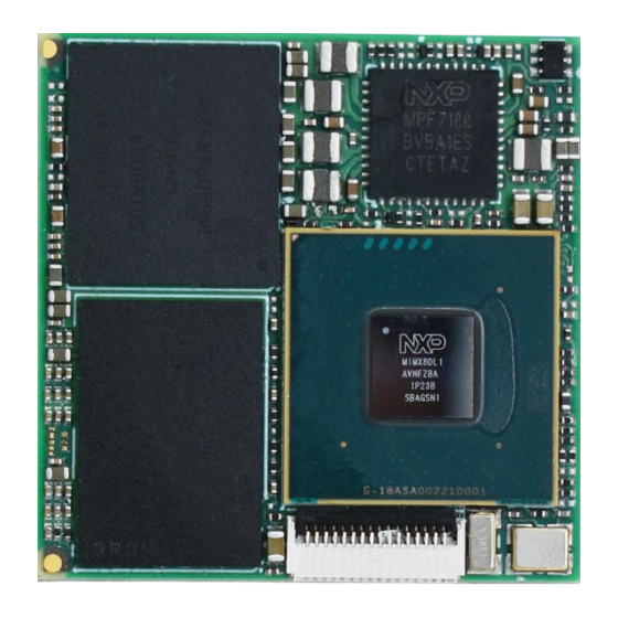
Summary of Contents for iWave iW-RainboW-G46M
- Page 1 8XLite OSM-Size SE LGA Module Hardware User Guide iW-RainboW-G46M i.MX 8XLite Dual/Solo OSM-Size SE LGA Module Hardware User Guide DRAFT VERSION SUBJECT TO CHANGE REL0.1 iWave Systems Technologies Pvt. Ltd. Page 1 of 52...
- Page 2 If you are not the intended recipient (or authorized to receive for the recipient), you are hereby notified that any disclosure, copying distribution or use of any of the information contained within this document is STRICTLY PROHIBITED. Thank you. “iWave Systems Tech. Pvt. Ltd.” REL0.1 iWave Systems Technologies Pvt.
- Page 3 No warranty of accuracy is given concerning the contents of the information contained in this publication. To the extent permitted by law no liability (including liability to any person by reason of negligence) will be accepted by iWave Systems, its subsidiaries or employees for any direct or indirect loss or damage caused by omissions from or inaccuracies in this document.
-
Page 4: Table Of Contents
TECHNICAL SPECIFICATION ..........................45 Electrical Characteristics ..........................45 3.1.1 Power Input Requirement ........................45 3.1.2 Power Consumption ..........................46 Environmental Characteristics ........................47 3.2.1 Environmental Specification ........................47 3.2.2 Heat Sink ............................... 47 REL0.1 iWave Systems Technologies Pvt. Ltd. Page 4 of 52... - Page 5 3.2.4 Electrostatic Discharge ........................... 48 Mechanical Characteristics ........................49 3.3.1 i.MX 8XLite OSM LGA Module Mechanical Dimensions ................49 ORDERING INFORMATION ..........................50 APPENDIX ................................. 51 i.MX 8XLite OSM Development Platform ....................51 REL0.1 iWave Systems Technologies Pvt. Ltd. Page 5 of 52...
- Page 6 Table 5: i.MX 8XLite SoC IOMUX for OSM LGA interfaces ..................38 Table 6: Power Input Requirement ..........................45 Table 7: Power Consumption ............................ 46 Table 8: Environmental Specification ........................47 Table 9: Orderable Product Part Numbers ......................... 50 REL0.1 iWave Systems Technologies Pvt. Ltd. Page 6 of 52...
-
Page 7: Introduction
This document is the Hardware User Guide for the NXP’s i.MX 8XLite (Dual/Solo) Application processor based OSM v1.0 specification compatible LGA module. This board is fully supported by iWave Systems Technologies Pvt. Ltd. This Guide provides detailed information on the overall design and usage of the i.MX 8XLite OSM Module from a Hardware Systems perspective. -
Page 8: Terminology Description
Universal Asynchronous Receiver/Transmitter Universal Serial Bus Video Processing Unit Terminology Description In this document, wherever Signal Type is mentioned, below terminology is used. Table 2: Terminology Terminology Description Input Signal REL0.1 iWave Systems Technologies Pvt. Ltd. Page 8 of 52... -
Page 9: References
Note: Signal Type does not include internal pull-ups or pull-downs implemented by the chip vendors and only includes the pull-ups or pull-downs implemented On-OSM. References • IMX8DXLA1AEC_Revx.pdf • iMX8DXL_RM_Rev_x.pdf • OSM Specification V1.0 REL0.1 iWave Systems Technologies Pvt. Ltd. Page 9 of 52... -
Page 10: Important Note
In this signal, BCONFIG_0 is the GPIO functionality and GPIO1_05 is the GPIO number. Note: The above naming is not applicable for other signals which are not connected to SoC. REL0.1 iWave Systems Technologies Pvt. Ltd. Page 10 of 52... -
Page 11: Architecture And Design
2. ARCHITECTURE AND DESIGN This section provides detailed information about i.MX 8XLite OSM LGA Module SOM and Hardware architecture with high level block diagram. i.MX 8XLite OSM LGA Module Block Diagram iW-RainboW-G46M- i.MX 8XLite based OSM Block Diagram On-Board Power to i.MX 8XLite... -
Page 12: I.mx 8Xlite Som Features
: 5V, 2.5A • Form Factor : 30mm X 30mm (OSM V1.0 Specification) Memory Size will differ based on iWave’s SOM Product Part Number. By default, only 1 Data UART port is supported. 2 UART is muxed with CAN. REL0.1 iWave Systems Technologies Pvt. -
Page 13: I.mx 8Xlite Soc
8XLite OSM-Size SE LGA Module Hardware User Guide i.MX 8XLite SoC iW-RainboW-G46M OSM LGA Module can support i.MX 8XLite SoCs from NXP. The i.MX 8XLite Family consists of two processors: i.MX 8XLite Dual & i.MX 8XLite Solo. The Major Difference between i.MX 8XLite SoCs are: •... -
Page 14: Pf7100 Pmic
I2C after start up offering flexibility for different system states. The PF7100 PMIC comes in 48pin 7x7 QFN Package and is placed on the Top side of the Module. REL0.1 iWave Systems Technologies Pvt. Ltd. Page 14 of 52... -
Page 15: Memory
The eMMC flash memory (U3) is physically located on Top side of the Module. The memory size of the eMMC Flash can be customised based on the requirement by contacting iWave Support Team. REL0.1 iWave Systems Technologies Pvt. Ltd. -
Page 16: Osm Lga Balls
OSM LGA has standard pinout as per OSM Specification V1.0 The interfaces which are available at 332 contacts are explained in the following sections. Figure 3: OSM LGA Number of contacts - : 332 REL0.1 iWave Systems Technologies Pvt. Ltd. Page 16 of 52... -
Page 17: Table 3: Osm Pinouts
8XLite OSM-Size SE LGA Module Hardware User Guide Table 3: OSM Pinouts OSM Pins Signal SIZE 0 BOOT_MODE0 AB17 FLEXCAN1_RX AC17 FLEXCAN1_TX AB19 FLEXCAN2_RX AC19 FLEXCAN2_TX CARRIER_PWR_ON AC18 ENET0_QOS_RGMII_RXC ENET0_QOS_RGMII_RX_CTL ENET0_QOS_RGMII_RD2 ENET0_QOS_RGMII_RD3 ENET0_QOS_RGMII_TXC ENET0_QOS_RGMII_TX_CTL ENET0_QOS_RGMII_TD2 ENET0_QOS_RGMII_TD3 ENET0_QOS_RGMII_RD0 REL0.1 iWave Systems Technologies Pvt. Ltd. Page 17 of 52... - Page 18 8XLite OSM-Size SE LGA Module Hardware User Guide OSM Pins Signal ENET0_QOS_RGMII_RD1 ENET0_QOS_RGMII_TD0 ENET0_QOS_RGMII_TD1 ENET_QOS_MDC ENET_QOS_MDIO AA14 AA17 AA19 AA22 AB15 AB21 GPIO3_IO20(QSPI0B_DATA2) GPIO3_IO21(QSPI0B_DATA3) GPIO3_IO18(QSPI0B_DATA0) GPIO3_IO19(QSPI0B_DATA1) GPIO3_IO22(QSPI0B_DQS) GPIO3_IO23(QSPI0B_SS0_B) GPIO3_IO17(QSPI0B_SCLK) GPIO3_IO16(QSPI0A_SCLK) GPIO3_IO14(QSPI0A_SS0_B) GPIO3_IO09(QSPI0A_DATA0) GPIO3_IO10(QSPI0A_DATA1) GPIO3_IO11(QSPI0A_DATA2) GPIO3_IO12(QSPI0A_DATA3) REL0.1 iWave Systems Technologies Pvt. Ltd. Page 18 of 52...
- Page 19 8XLite OSM-Size SE LGA Module Hardware User Guide OSM Pins Signal ENET0_REFCLK_125M_25M AA15 I2C2_SCL(SPI1_SDO) AA16 I2C2_SDA(SPI1_SCK) AA20 I2C3_SCL(SPI1_SDI) AA21 I2C3_SDA(SPI1_CS0) SAI1_RXD(FLEXCAN1_TX) SAI1_TXD(FLEXCAN1_RX) SAI1_TXC(FLEXCAN0_RX) SAI1_TXFS(FLEXCAN0_TX) JTAG_NTRST JTAG_TCK JTAG_TDI JTAG_TDO JTAG_TMS BOOT_MODE1 AA13 VDD_RTC REL0.1 iWave Systems Technologies Pvt. Ltd. Page 19 of 52...
- Page 20 8XLite OSM-Size SE LGA Module Hardware User Guide OSM Pins Signal SPI2_CSO(USDHC1_CD_B) SPI2_SCK(USDHC1_RESET_B) SPI2_SDI(USDHC1_WP) SPI2_SDO(USDHC1_VSELECT) AA23 SYS_RST# ADMA_UART3_RX ADMA_UART3_TX UART2_RX UART2_TX UART0_RX UART0_TX REL0.1 iWave Systems Technologies Pvt. Ltd. Page 20 of 52...
- Page 21 AC16 USB_OTG1_PWR(USB_SS3_TC0) AB14 USB_OTG1_ID AC15 USB_OTG1_OC(USB_SS3_TC2) AB16 OTG1_VBUS AB23 USB_OTG2_DM AC22 USB_OTG2_DP AC20 USB_OTG2_PWR(USB_SS3_TC1) AB22 USB_OTG2_ID AC21 USB_OTG2_OC(USB_SS3_TC3) AB20 OTG2_VBUS AA18 AB18 VDD_MAIN_1V0 VDD_MEMC_1V1 VDD_PER_1V8 VCC_3V3 VCC_IN_5V PMIC_ON_REQ SIZE S REL0.1 iWave Systems Technologies Pvt. Ltd. Page 21 of 52...
- Page 22 8XLite OSM-Size SE LGA Module Hardware User Guide OSM Pins Signal AB11 AB10 ENET1_RGMII_RXC ENET1_RGMII_RX_CTL ENET1_RGMII_RD2 ENET1_RGMII_RD3 ENET1_RGMII_TXC ENET1_RGMII_TX_CTL ENET1_RGMII_TD2 ENET1_RGMII_TD3 ENET1_RGMII_RD0 ENET1_RGMII_RD1 ENET1_RGMII_TD0 ENET1_RGMII_TD1 AC10 AA11 AA10 REL0.1 iWave Systems Technologies Pvt. Ltd. Page 22 of 52...
- Page 23 8XLite OSM-Size SE LGA Module Hardware User Guide OSM Pins Signal ENET1_REFCLK_125M_25M PCIE0_A_RX0_N PCIE0_A_RX0_P PCIE0_A_TX0_N PCIE0_A_TX0_P PCIE_RST_B PCIE_CLKREQ_B PCIE_CPU_REFCLK100M_N PCIE_CPU_REFCLK100M_P GPIO3_IO13(QSPI0A_DQS) I2C2_SCL(SPI1_SDO) I2C2_SDA(SPI1_SCK) PCIE_WAKE_B REL0.1 iWave Systems Technologies Pvt. Ltd. Page 23 of 52...
- Page 24 OSM Pins Signal CPU_ON_OFF ADMA_LCDIF_CLK(MCLK_OUT0) ADMA_LCDIF_D00_B0(SPI3_SCK) ADMA_LCDIF_D01_B1(SPI3_SDO) ADMA_LCDIF_D02_B2(SPI3_SDI) ADMA_LCDIF_D03_B3(MCLK_IN0) ADMA_LCDIF_D04_B4(UART1_TX) ADMA_LCDIF_D05_B5(UART1_RX) ADMA_LCDIF_RDE(SPI3_CS1) ADMA_LCDIF_D06_G0(UART1_RTS_B) ADMA_LCDIF_D07_G1(UART1_CTS_B) ADMA_LCDIF_D08_G2(SPI0_SCK) ADMA_LCDIF_D09_G3(SPI0_SDI) ADMA_LCDIF_D10_G4(SPI0_SDO) ADMA_LCDIF_D11_G5(SPI0_CS1) ADMA_LCDIF_HSYNC(SPI3_CS0) ADMA_LCDIF_D12_R0(SPI0_CS0) ADMA_LCDIF_D13_R1(ADC_IN1)_3V3 ADMA_LCDIF_D14_R2(ADC_IN0)_3V3 ADMA_LCDIF_D15_R3(ADC_IN3)_3V3 ADMA_LCDIF_D16_R4(ADC_IN2)_3V3 ADMA_LCDIF_D17_R5(ADC_IN5)_3V3 ADMA_LCDIF_RESET(ADC_IN4)_3V3 ADMA_LCDIF_VSYNC(MCLK_IN1) VDD_CPU_1V8 VDD_DDR_1V1 VCC_IN_5V REL0.1 iWave Systems Technologies Pvt. Ltd. Page 24 of 52...
- Page 25 8XLite OSM-Size SE LGA Module Hardware User Guide OSM Pins Signal VCC_IN_5V VCC_IN_5V VCC_IN_5V GPIO2_IO05(SNVS_TAMPER_OUT1) GPIO2_IO10(SNVS_TAMPER_IN1) SNVS_TAMPER_IN4 SNVS_TAMPER_OUT0 REL0.1 iWave Systems Technologies Pvt. Ltd. Page 25 of 52...
-
Page 26: Rgmii Interface
ENET0_QOS_RG ENET0_RGMII_RX_C I CMOS Receive data valid port A _RX_DV(_ER) MII_RX_CTL TL/C33 ETH_A_(R)(G)MII ENET0_QOS_RG ENET0_RGMII_RXC/ I/O CMOS Receive clock port A _RX_CLK MII_RXC ETH_MDIO ENET_QOS_MDIO ENET0_MDIO/E35 I/O CMOS Management data REL0.1 iWave Systems Technologies Pvt. Ltd. Page 26 of 52... - Page 27 ETH_B_(R)(G)MII_R ENET1_RGMII_RX ENET1_RGMII_RXC/ I/O CMOS Receive clock port B X_CLK Note: On-OSM series termination resistors for ENET0_TX & ENET1_TX is not provided. Kindly provide the same in the Carrier Board. REL0.1 iWave Systems Technologies Pvt. Ltd. Page 27 of 52...
-
Page 28: Usb 2.0 Otg Interface
USB 2.0 Port1 Over Current USB_SS3_TC3) 10K PU Indicator. AB20 USB_B_VBUS OTG2_VBUS USB_OTG2_VBU I USB VBUS 5V USB Port1 power detection. S/G13 AC20 USB_B_EN USB_OTG2_PW USB_SS3_TC1/G O, 3.3V CMOS USB Power Enable. R(USB_SS3_TC1 REL0.1 iWave Systems Technologies Pvt. Ltd. Page 28 of 52... -
Page 29: Pcie Interface
I2S, AC97 and other audio CODEC/DSP interfaces. The SAI general features are including Transmitter section with independent REL0.1 iWave Systems Technologies Pvt. Ltd. Page 29 of 52... -
Page 30: Spi Interface
LGA balls whereas UART2 is optionally connected to the LGA. UART3 can be used for any data communication. UART0 of the SoC is connected to LGA and used as Debug UART. For more details on UART pinouts, refer below table: REL0.1 iWave Systems Technologies Pvt. Ltd. Page 30 of 52... -
Page 31: Can Interface
Pin Number AC17 CAN_A_TX FLEXCAN1_TX(UART2_TX UART2_TX/AP O, 1.8V CAN 1 Transmitter. CMOS AB17 CAN_A_RX FLEXCAN1_RX(UART2_RX UART2_RX/AN I, 1.8V CAN 1 Receiver. CMOS AC19 CAN_B_TX FLEXCAN2_TX FLEXCAN2_TX O, 1.8V CAN 2 Transmitter. REL0.1 iWave Systems Technologies Pvt. Ltd. Page 31 of 52... -
Page 32: Rgb Interface
ADC_IN1/AE35 O, 3.3V RGB_R1 DC_IN1)_3V3 CMOS Red data bit 1 ADMA_LCDIF_D14_R2(A ADC_IN0/AD3 O, 3.3V RGB_R2 DC_IN0)_3V3 CMOS Red data bit 2 ADMA_LCDIF_D15_R3(A ADC_IN3/AF34 O, 3.3V RGB_R3 DC_IN3)_3V3 CMOS Red data bit 3 REL0.1 iWave Systems Technologies Pvt. Ltd. Page 32 of 52... -
Page 33: Jtag Interface
I2C2 Data. AP16 CMOS 2.2K PU AA20 I2C_B_SCL I2C3_SCL(SPI1_SDI) SPI1_SDI/ O, 1.8V I2C3 Clock. AP18 CMOS 2.2K PU AA21 I2C_B_SDA I2C3_SDA(SPI1_CS0) SPI1_CS0/ IO, 1.8V I2C3 Data. AR15 CMOS 2.2K PU REL0.1 iWave Systems Technologies Pvt. Ltd. Page 33 of 52... -
Page 34: Osm Gpios
/AN11 CMOS Input/output B4. GPIO_B_6 ENET0_REFCLK_125 ENET0_REFCLK IO, 1.8V OSM General Purpose M_25M _125M_25M/D CMOS Input/output B6. GPIO_C_2 ENET1_REFCLK_125 ENET1_REFCLK IO, 1.8V OSM General Purpose M_25M _125M_25M/K CMOS Input/output C2. REL0.1 iWave Systems Technologies Pvt. Ltd. Page 34 of 52... -
Page 35: Control Signals
For more details on Power & GND Signals pinouts on OSM PCB Ball, refer the below table. SoC Ball OSM Pin OSM Signal Signal Type/ Pin No. Name/ Description Name Name Termination Pin Number Y8, Y9, Y10, Y11, Y17 VCC_IN_5V VCC_IN_5V I, 5V Power Supply Voltage. REL0.1 iWave Systems Technologies Pvt. Ltd. Page 35 of 52... - Page 36 POWER voltage test point D18,E15,E21,F16,F2 Power Ground. 0,J16,J20,L18,M16, M20,P18,R16,R20,V 16,V20,Y18,AA14,A A17,AA19,AA22,AB1 5,AB21,A4,A7,A10,B 2,B5,B8,B9,C11,D1,D 5,D8,E2,H2,H4,L2,L4, P2,P4,R1,U2,U4,V1, W3,Y2,AA1,AA4,AA 7,AA8,AA10,AA11,A B3,AB6,AB9,AC4,AC 7,AC10 VDD_RTC VDD_RTC I, 3V Power 3V coin cell input for RTC. REL0.1 iWave Systems Technologies Pvt. Ltd. Page 36 of 52...
-
Page 37: Other Features
USB VBUS power for detection. Power Ground UART0_RX O, 1.8V CMOS Debug UART Receiver. UART0_TX I, 1.8V CMOS Debug UART Transmitter. Power Ground Power Ground BOOT_MODE0 SCU_BOOT_M I OD CMOS ,1.8V/4.7K PU ODE0/AR23 REL0.1 iWave Systems Technologies Pvt. Ltd. Page 37 of 52... -
Page 38: I.mx 8Xlite Pin Multiplexing On Osm Lga
This table has been prepared by referring NXP’s i.MX 8XLite Hardware User’s Manual. Important Note: It is strongly recommended to use the pin function same as selected in the OSM LGA for iWave’s BSP reusability and to have compatible OSM modules in future for upgradability. - Page 39 ADMA.UART3. ADMA.SAI1.RX ADMA.FLEXCAN2. LSIO.GPIO1.IO20 LSIO.GPIO6.IO13 AL33 AB16 CONN.USB_OTG1. CONN.USB_OTG1. VBUS VBUS AB14 CONN.USB_OTG1. CONN.USB_OTG1. AC14 CONN.USB_OTG1. CONN.USB_OTG1. OTG1 AB13 CONN.USB_OTG1. CONN.USB_OTG1. AC16 CONN.USB_OTG CONN.USB_O CONN.USB_OTG1. ADMA.I2C1.SCL LSIO.GPIO4.IO03 LSIO.GPIO7.IO03 1.PWR TG2.PWR REL0.1 iWave Systems Technologies Pvt. Ltd. Page 39 of 52...
- Page 40 LSIO.GPIO2.IO03 ADMA.UART3.RX AR27 AP26 M40.UART0.T ADMA.UART3. SCU.WDOG0.WD SCU.GPIO0.IO01 SCU.UART0.TX ADMA.UART3.TX OG_OUT ADMA.FLEXCAN0. ADMA.UART0. ADMA.SAI1.TX ADMA.SAI2.RXC LSIO.GPIO1.IO15 LSIO.GPIO6.IO08 ADMA.SAI1.TXC Audio AH34 RTS_B ADMA.FLEXCAN0. ADMA.UART0. ADMA.SAI1.TX ADMA.SAI2.RXD LSIO.GPIO1.IO16 LSIO.GPIO6.IO09 ADMA.SAI1.TXFS AJ35 CTS_B REL0.1 iWave Systems Technologies Pvt. Ltd. Page 40 of 52...
- Page 41 CONN.EQOS.RGM tiedoff input LSIO.GPIO0.IO09 LSIO.GPIO6.IO03 GMII_TXD1 II_TXD1 ADMA.LCDIF. CONN.EQOS.R CONN.EQOS.RGM ADMA.SPDIF0.RX ADMA.MQS.R LSIO.GPIO0.IO10 LSIO.GPIO6.IO04 GMII_RXD0 II_RXD0 ADMA.LCDIF. CONN.EQOS.R CONN.EQOS.RGM ADMA.SPDIF0.TX ADMA.MQS.L LSIO.GPIO0.IO11 LSIO.GPIO6.IO05 GMII_RX_CTL II_RX_CTL ADMA.LCDIF. ADMA.SPI3.SCK LSIO.GPIO0.IO13 ADMA.LCDIF.D00 ADMA.LCDIF.D00 REL0.1 iWave Systems Technologies Pvt. Ltd. Page 41 of 52...
- Page 42 M40.I2C0.SDA LSIO.GPIO1.IO06 ADMA.LCDIF.D10 ADMA.LCDIF.D10 AA35 ADMA.SAI1.TX ADMA.LCD_P ADMA.SPI0.CS1 ADMA.SAI0.RXC LSIO.GPIO1.IO07 ADMA.LCDIF.D11 ADMA.LCDIF.D11 AC35 WM0.OUT M40.TPM0.CH M40.GPIO0.IO ADMA.SPI0.CS0 ADMA.SAI0.RXD LSIO.GPIO1.IO08 ADMA.LCDIF.D12 ADMA.LCDIF.D12 AB34 M40.GPIO0.IO ADMA.I2C0.SD ADMA.ADC.IN1 M40.I2C0.SDA LSIO.GPIO1.IO09 ADMA.LCDIF.D13 ADMA.LCDIF.D13 AE35 REL0.1 iWave Systems Technologies Pvt. Ltd. Page 42 of 52...
- Page 43 HSIO.PCIE0.WAKE HSIO.PCIE0.TX0_P HSIO.PCIE0.TX0_P HSIO.PCIE0.TX0_ HSIO.PCIE0.TX0_ PCIe HSIO.PCIE0.RX0_P HSIO.PCIE0.RX0_P HSIO.PCIE0.RX0_ HSIO.PCIE0.RX0_ HSIO.PCIE_IOB.EX HSIO.PCIE_IOB.EX T_REFCLK100M_P T_REFCLK100M_P HSIO.PCIE_IOB.EX HSIO.PCIE_IOB.EX T_REFCLK100M_ T_REFCLK100M_ LSIO.QSPI0A.DAT LSIO.GPIO3.IO09 LSIO.GPIO3.IO09 AR11 LSIO.QSPI0A.DAT GPIO LSIO.GPIO3.IO10 LSIO.GPIO3.IO10 AN13 LSIO.QSPI0A.DAT LSIO.GPIO3.IO11 LSIO.GPIO3.IO11 REL0.1 iWave Systems Technologies Pvt. Ltd. Page 43 of 52...
- Page 44 LSIO.GPIO3.IO18 LSIO.GPIO3.IO18 AP10 LSIO.QSPI0B.DAT LSIO.GPIO3.IO19 LSIO.GPIO3.IO19 AP12 LSIO.QSPI0B.DAT LSIO.GPIO3.IO20 LSIO.GPIO3.IO20 AR13 LSIO.QSPI0B.DAT LSIO.GPIO3.IO21 LSIO.GPIO3.IO21 AP14 AN15 LSIO.QSPI0B.DQS LSIO.GPIO3.IO22 LSIO.GPIO3.IO22 LSIO.QSPI0B.SS0_ LSIO.GPIO3.IO23 LSIO.QSPI0A.SS1_B LSIO.GPIO3.IO23 AJ11 LSIO.QSPI0A.SCLK LSIO.GPIO3.IO16 LSIO.GPIO3.IO16 LSIO.QSPI0A.SS0_ LSIO.GPIO3.IO14 LSIO.GPIO3.IO14 REL0.1 iWave Systems Technologies Pvt. Ltd. Page 44 of 52...
-
Page 45: Technical Specification
¹ i.MX 8XLite OSM LGA Module is designed to work with VCC_IN_5V input power rail from OSM. i.MX 8XLite OSM LGA Module use this voltage as backup power source when VCC_IN_5V is OFF. REL0.1 iWave Systems Technologies Pvt. Ltd. Page 45 of 52... -
Page 46: Power Consumption
0.055/0.275 RTC power when no VCC_IN_5V supply is provided VRTC_3V0 0.0000004/0.0000012 ¹ Power consumption measurements have been done in iWave’s i.MX 8XLite based Pico ITX SBC with iWave‘s iW- PRGWZ-SC-01-R2.0-REL1.0-Linux5.15.52 BSP. REL0.1 iWave Systems Technologies Pvt. Ltd. Page 46 of 52... -
Page 47: Environmental Characteristics
SoC. Note: iWave supports Heat Sink Solution for i.MX 8XLite OSM LGA Module. For more information on Heat Sink contact iWave support team. Do not Power On the SOM without a proper thermal solution. -
Page 48: Rohs Compliance
3.2.4 Electrostatic Discharge iWave’s i.MX 8XLite OSM LGA Module is sensitive to electro static discharge and so high voltages caused by static electricity could damage some of the devices on board. It is packed with necessary protection while shipping. Do not open or use the SOM except at an electrostatic free workstation. -
Page 49: Mechanical Characteristics
The i.MX 8XLite OSM LGA Module PCB thickness is 1.2mm±0.1mm, top side maximum height component is 1.87mm (Programming Header). In bottom side maximum height component is Voltage Level Translator (1mm). Please refer the above figure which gives height details of the i.MX 8XLite OSM LGA Module. REL0.1 iWave Systems Technologies Pvt. Ltd. Page 49 of 52... -
Page 50: Ordering Information
The below table provides the standard orderable part numbers for different i.MX 8XLite OSM LGA Module variants. Please contact iWave for orderable part number of higher RAM memory size or Flash memory size SOM configurations. Also, if the desired part number is not listed in below table or if any custom configuration part number is required, please contact iWave. -
Page 51: Appendix
8XLite Pico ITX SBC iWave Systems supports iW-RainboW-G46S-i.MX 8XLite Pico ITX SBC which is targeted for quick validation of i.MX 8XLite SoC based OSM and its features. Being a Pico-ITX form factor with 100mm x 72mm size, the SBC is highly packed with all necessary interfaces &... - Page 52 8XLite OSM-Size SE LGA Module Hardware User Guide REL0.1 iWave Systems Technologies Pvt. Ltd. Page 52 of 52...
Need help?
Do you have a question about the iW-RainboW-G46M and is the answer not in the manual?
Questions and answers