
Subscribe to Our Youtube Channel
Related Manuals for iWave iW-RainboW-G50M i.MX 93


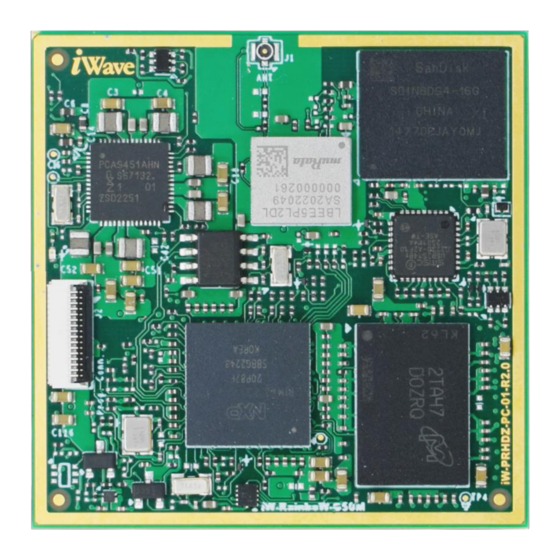
Summary of Contents for iWave iW-RainboW-G50M i.MX 93
- Page 1 93 or i.MX 91 OSM-Size LF LGA Module Hardware User Guide iW-RainboW-G50M i.MX 93 or i.MX 91 OSM-LF LGA Module Hardware User Guide DRAFT VERSION SUBJECT TO CHANGE REL0.2 iWave Systems Technologies Pvt. Ltd. Page 1 of 69...
- Page 2 If you are not the intended recipient (or authorized to receive for the recipient), you are hereby notified that any disclosure, copying distribution or use of any of the information contained within this document is STRICTLY PROHIBITED. Thank you. “iWave Systems Tech. Pvt. Ltd.” REL0.2 iWave Systems Technologies Pvt.
- Page 3 No warranty of accuracy is given concerning the contents of the information contained in this publication. To the extent permitted by law no liability (including liability to any person by reason of negligence) will be accepted by iWave Systems, its subsidiaries or employees for any direct or indirect loss or damage caused by omissions from or inaccuracies in this document.
-
Page 4: Table Of Contents
2.7.16 Control Signals ............................51 2.7.17 Power and GND ............................. 51 Other Features ............................53 2.8.1 Programming Header..........................53 i.MX 93 or i.MX 91 Pin Multiplexing on OSM LGA ..................55 REL0.2 iWave Systems Technologies Pvt. Ltd. Page 4 of 69... - Page 5 3.3.1 i.MX 93 or i.MX 91 OSM LGA Module Mechanical Dimensions ..............65 ORDERING INFORMATION ..........................66 APPENDIX-I ............................... 67 i.MX 93 or i.MX 91 SBC ..........................67 APPENDIX-II ..............................68 Design and Assembly recommendations ....................68 REL0.2 iWave Systems Technologies Pvt. Ltd. Page 5 of 69...
- Page 6 Table 7: i.MX 93 OSM Power Consumption ....................... 61 Table 7: i.MX 91 OSM Power Consumption ....................... 62 Table 8: Environmental Specification ........................63 Table 9: Orderable Product Part Numbers ......................... 66 REL0.2 iWave Systems Technologies Pvt. Ltd. Page 6 of 69...
-
Page 7: Introduction
This document is the Hardware User Guide for the NXP’s i.MX 93 or i.MX 91 Application processor based OSM V1.1 specification compatible LGA module. This board is fully supported by iWave Systems Technologies Pvt. Ltd. This Guide provides detailed information on the overall design and usage of the i.MX 93 or i.MX 91 OSM Module from a Hardware Systems perspective. - Page 8 Real Time Clock Request to Send Serial Audio Interface Secure Digital System on Chip System On Module SPDIF The Sony/Philips Digital Interface Serial Peripheral Interface UART Universal Asynchronous Receiver/Transmitter Universal Serial Bus REL0.2 iWave Systems Technologies Pvt. Ltd. Page 8 of 69...
-
Page 9: Terminology Description
Note: Signal Type does not include internal pull-ups or pull-downs implemented by the chip vendors and only includes the pull-ups or pull-downs implemented On-OSM. References • IMX93IEC_Rev_x.pdf • IMX91PEC_Revx • i.MX93RM Rev_x.pdf • OSM Specification V1.1 REL0.2 iWave Systems Technologies Pvt. Ltd. Page 9 of 69... -
Page 10: Important Note
In this signal, BCONFIG_0 is the GPIO functionality and GPIO1_05 is the GPIO number. Note: The above naming is not applicable for other signals which are not connected to SoC. REL0.2 iWave Systems Technologies Pvt. Ltd. Page 10 of 69... -
Page 11: Architecture And Design
If Wi-Fi/BT is required, SPI is not supported at OSM. * Not supported in i.MX 91 SoC VRTC_3V mktg@iwavesystems.com iWave Systems Technologies Pvt. Ltd. Figure 1: i.MX 93 or i.MX 91 OSM LGA MODULE Block Diagram REL0.2 iWave Systems Technologies Pvt. Ltd. -
Page 12: I.mx 93 And I.mx 91 Som Features
SPI x 1 • Data UART with flow control x 2 (1 is optional) • Data UART without flow control x 1 • Debug UART x 1 • GPIOs x 16 REL0.2 iWave Systems Technologies Pvt. Ltd. Page 12 of 69... - Page 13 There are four configurations of i.MX 93 Processor, hence this document is used to represent either of one based on SOM Part Number. Memory Size will differ based on iWave’s SOM Product Part Number. i.MX 93 OSM supports LPDDR4X by default and i.MX 91 OSM supports LPDDR4.
-
Page 14: Cpu
93 or i.MX 91 OSM-Size LF LGA Module Hardware User Guide iW-RainboW-G50M i.MX 93 and i.MX 91 OSM LGA Module can support different i.MX 93 or i.MX 91 SoCs from NXP. 2.3.1 i.MX 93 CPU The i.MX 93 (11 x 11 mm) Family consists of four processors. -
Page 15: I.mx 91 Cpu
Note: The i.MX 93 and i.MX 91 processor offers numerous advanced features, please refer the latest i.MX 93 or i.MX 91 Datasheet & Reference Manual for Electrical characteristics and other information, which may be revised from time to time. REL0.2 iWave Systems Technologies Pvt. Ltd. Page 15 of 69... -
Page 16: Pca9451 Pmic
5V adapter non-portable applications. Regulator parameters are adjustable through high-speed I2C after start up offering flexibility for different system states. The PCA9451 PMIC comes in 56-pin HVQFN package. REL0.2 iWave Systems Technologies Pvt. Ltd. Page 16 of 69... -
Page 17: Memory
The i.MX 93 or i.MX 91 OSM LGA Module supports 2GB LPDDR4X/LPDDR4 memory by using 16bit DDR_CH0 channel of the SoC. By default, LPDDR4X is supported in i.MX 93 OSM. The i.MX 91 SoC supports only LPDDR4. To customize the LPDDR4X/LPDDR4 memory size, contact iWave. 2.5.2 eMMC Flash The i.MX 93 or i.MX 91 OSM LGA Module supports 16GB eMMC as default boot and storage device. -
Page 18: Network & Communications Features
OSM. If SPI is required at the OSM, Wi-Fi/BT module will be made DNP in the OSM. Figure 4: Wi-Fi+Bluetooth Antenna Connector Connector Part Number - : MM4829-2702RA4 from Murata. Antenna Part Number - : 2042811100 from Molex REL0.2 iWave Systems Technologies Pvt. Ltd. Page 18 of 69... -
Page 19: Rtc Controller
1.8V voltage level. In SOM power off condition, this device will take power from OSM pin No. W17 (RTC_PWR) coin cell power input and continues to keep the current time. Note: RTC cannot be used as wake-up source, as a result RTC alarm won't work. REL0.2 iWave Systems Technologies Pvt. Ltd. Page 19 of 69... -
Page 20: Osm Lga/Bga
OSM LGA/BGA (J3) has standard pinout as per OSM Specification V1.1 The interfaces which are available at 662 contacts are explained in the following sections. Figure 5: OSM LGA/BGA Number of contacts - : 662 REL0.2 iWave Systems Technologies Pvt. Ltd. Page 20 of 69... -
Page 21: Table 3: Osm Pinouts
Table 3: OSM Pinouts OSM Pins Signal SIZE 0 ADC_IN0 ADC_IN1 BOOT_SEL0# UART2_TXD(BOOT_MODE1) AB17 CAN1_RX(PDM_BIT0) AC17 CAN1_TX(PDM_CLK) AB19 CAN2_RX(GPIO_IO27) AC19 CAN2_TX(GPIO_IO25) CARRIER_PWR_ON OSM_ANT0 AC18 ENET1_QOS_RGMII_RXC ENET1_QOS_RGMII_RX_CTL ENET1_QOS_RGMII_RD2 ENET1_QOS_RGMII_RD3 ENET1_QOS_RGMII_TXC ENET1_QOS_RGMII_TX_CTL ENET1_QOS_RGMII_RD0 ENET1_QOS_RGMII_RD1 REL0.2 iWave Systems Technologies Pvt. Ltd. Page 21 of 69... - Page 22 93 or i.MX 91 OSM-Size LF LGA Module Hardware User Guide OSM Pins Signal ENET1_QOS_RGMII_TD0 ENET1_QOS_RGMII_TD1 ENET1_QOS_RGMII_TD2 ENET1_QOS_RGMII_TD3 VDD_1V8 ENET1_QOS_MDC ENET1_QOS_MDIO FORCE_RECOV# AA14 AA17 AA19 AA22 AB15 AB21 OSM_GPIO_A0(GPIO1_IO01_I3C1_SDA) OSM_GPIO_A1(SPI3_MISO_GPIO_IO09) OSM_GPIO_A2(SPI3_MOSI_GPIO_IO10) OSM_GPIO_A3(SPI3_SS0_GPIO_IO08) OSM_GPIO_A4(SPI3_SCLK_GPIO_IO11) OSM_GPIO_A5(GPIO1_IO00_I3C1_SCL) OSM_GPIO_A6(IO_5) OSM_GPIO_A7(GPIO4_IO29_CCM_CLKO4) OSM_GPIO_B0(GPIO4_IO28_CCM_CLKO3) OSM_GPIO_B1(GPIO_IO16) REL0.2 iWave Systems Technologies Pvt. Ltd. Page 22 of 69...
- Page 23 OSM Pins Signal OSM_GPIO_B2(GPIO_IO17) OSM_GPIO_B5(GPIO_IO26) AA15 I2C7_SCL(GPIO_IO07) AA16 I2C7_SDA(GPIO_IO06) AA20 I2C3_SCL(GPIO_IO29) AA21 I2C3_SDA(GPIO_IO28) SAI1_RX_DATA0 SAI1_TXD0(BOOT_MODE3) SAI1_TXCLK SAI1_TXFS(BOOT_MODE2) JTAG_NTRST GPIO3_IO30(JTAG_TCK) GPIO3_IO28(JTAG_TDI) GPIO3_IO31(JTAG_TDO) GPIO3_IO29(JTAG_TMS) AA13 VRTC_3V0 SD2_CD_B SD2_CLK SD2_CMD SD2_DATA0 SD2_DATA1 SD2_DATA2 REL0.2 iWave Systems Technologies Pvt. Ltd. Page 23 of 69...
- Page 24 93 or i.MX 91 OSM-Size LF LGA Module Hardware User Guide OSM Pins Signal SD2_DATA3 NVCC_SD2 GPIO3_IO7(SD2_RESET_B) SDIO_B_IOPWR SPI4_SSO(GPIO_IO18) SPI4_SCK(GPIO_IO21) SPI4_MISO(GPIO_IO19) SPI4_MOSI(GPIO_IO20) AA23 PMIC_RST_B UART5_CTS(GPIO_IO02) UART5_RTS(GPIO_IO03) UART5_RXD(GPIO_IO01) UART5_TXD(GPIO_IO00) UART8_CTS UART8_RTS UART8_RXD UART8_TXD UART2_RXD UART2_TXD(BOOT_MODE1) UART1_RXD REL0.2 iWave Systems Technologies Pvt. Ltd. Page 24 of 69...
- Page 25 AB22 USB_B_ID AC21 OSM_USB_B_OC AB20 USB_B_VBUS AB18 V_BAT AA18 V_BAT VDD_3V3 NVCC_SD2 VDD_SOC_0V8 VCC_IN_3V3 VCC_IN_5V VCC_OUT_IO PMIC_ON_REQ ADC_IN2 ADC_IN3 SIZE S CAM_PWR_EN(GPIO_IO24) CAM_RST(GPIO_IO23) MIPI_CSI1_CLK_N* MIPI_CSI1_CLK_P* MIPI_CSI1_D0_N* MIPI_CSI1_D0_P* MIPI_CSI1_D1_N* MIPI_CSI1_D1_P* MIPI_DSI1_CLK_N* REL0.2 iWave Systems Technologies Pvt. Ltd. Page 25 of 69...
- Page 26 OSM Pins Signal MIPI_DSI1_CLK_P* AB11 MIPI_DSI1_D0_N* AB10 MIPI_DSI1_D0_P* MIPI_DSI1_D1_N* MIPI_DSI1_D1_P* MIPI_DSI1_D2_N* MIPI_DSI1_D2_P* MIPI_DSI1_D3_N* MIPI_DSI1_D3_P* ENET2_RGMII_RXC ENET2_RGMII_RX_CTL ENET2_RGMII_RD2 ENET2_RGMII_RD3 ENET2_RGMII_TXC ENET2_RGMII_TX_CTL ENET2_RGMII_RD0 ENET2_RGMII_RD1 ENET2_RGMII_TD0 ENET2_RGMII_TD1 ENET2_RGMII_TD2 ENET2_RGMII_TD3 ENET2_MDC ENET2_MDIO AC10 AA11 AA10 REL0.2 iWave Systems Technologies Pvt. Ltd. Page 26 of 69...
- Page 27 93 or i.MX 91 OSM-Size LF LGA Module Hardware User Guide OSM Pins Signal OSM_GPIO_C4(GPIO_IO22) GPIO2_IO4(GPIO_IO04) I2C7_SCL(GPIO_IO07) I2C7_SDA(GPIO_IO06) REL0.2 iWave Systems Technologies Pvt. Ltd. Page 27 of 69...
- Page 28 93 or i.MX 91 OSM-Size LF LGA Module Hardware User Guide OSM Pins Signal CPU_ON_OFF USB_HUB2OUT_DM USB_HUB2OUT_DP OSM_USBC_PWR_EN USB_C_ID OSMC_USB_OC VCC_5_TEST REL0.2 iWave Systems Technologies Pvt. Ltd. Page 28 of 69...
- Page 29 93 or i.MX 91 OSM-Size LF LGA Module Hardware User Guide OSM Pins Signal VCC_6_TEST VCC_IN_5V VCC_IN_5V VCC_IN_5V VCC_IN_5V TAMPER0 TAMPER1 SIZE M AB35 AC34 REL0.2 iWave Systems Technologies Pvt. Ltd. Page 29 of 69...
- Page 30 93 or i.MX 91 OSM-Size LF LGA Module Hardware User Guide OSM Pins Signal AA35 AA34 AC30 AC33 AC27 AB34 AB31 AB28 AA32 AA28 AA27 AA26 AA25 REL0.2 iWave Systems Technologies Pvt. Ltd. Page 30 of 69...
- Page 31 93 or i.MX 91 OSM-Size LF LGA Module Hardware User Guide OSM Pins Signal AB25 AB26 AC26 AB27 AC32 REL0.2 iWave Systems Technologies Pvt. Ltd. Page 31 of 69...
- Page 32 93 or i.MX 91 OSM-Size LF LGA Module Hardware User Guide OSM Pins Signal AC31 AB33 AB32 AC29 AC28 AB30 AB29 USB_HUB3OUT_DM USB_HUB3OUT_DP OSM_USBD_PWR_EN USB_D_ID OSM_USB_D_OC AA33 VCC_IN_5V VCC_IN_5V VCC_IN_5V VCC_IN_5V USB_HUB4OUT_DP AA29 USB_HUB4OUT_DM AA30 AA31 SIZE L REL0.2 iWave Systems Technologies Pvt. Ltd. Page 32 of 69...
- Page 33 93 or i.MX 91 OSM-Size LF LGA Module Hardware User Guide OSM Pins Signal AN10 AR10 AP25 AP28 AP31 AP34 AR14 AP19 AR20 AR26 AR29 AR32 AP22 AP16 AP13 AE34 AN33 AN21 REL0.2 iWave Systems Technologies Pvt. Ltd. Page 33 of 69...
- Page 34 AF33 AG32 AG33 AH32 AH33 AJ32 AJ33 AN12 LVDS0_CLK_N* AN13 LVDS0_CLK_P* AP17 LVDS0_D0_N* AP18 LVDS0_D0_P* AR15 LVDS0_D1_N* AR16 LVDS0_D1_P* AP14 LVDS0_D2_N* AP15 LVDS0_D2_P* AP11 LVDS0_D3_N* AP12 LVDS0_D3_P* AN16 AN17 AM20 REL0.2 iWave Systems Technologies Pvt. Ltd. Page 34 of 69...
- Page 35 AN14 AP32 AP33 AP35 AN35 AL35 AK35 AH35 AG35 AR33 AR34 AN34 AM34 AK34 AJ34 AG34 AF34 AE33 AR18 AR19 AR21 AR22 AP26 AP27 AP29 AP30 AP20 AP21 AP23 AP24 REL0.2 iWave Systems Technologies Pvt. Ltd. Page 35 of 69...
- Page 36 OSM Pins Signal AR27 AR28 AR30 AR31 AN32 AM10 AM23 AM24 AM25 AM26 AM27 AM28 AM29 AM30 AM31 AN24 AN25 AN26 AN27 AN28 AN29 AN30 AP10 AN31 AE32 VCC_IN_5V VCC_IN_5V VCC_IN_5V REL0.2 iWave Systems Technologies Pvt. Ltd. Page 36 of 69...
- Page 37 93 or i.MX 91 OSM-Size LF LGA Module Hardware User Guide OSM Pins Signal VCC_IN_5V VCC_IN_5V VCC_IN_5V VCC_IN_5V VCC_IN_5V AK32 AK33 AL32 AL33 AM32 AM33 * Not supported in i.MX 91 SoC. REL0.2 iWave Systems Technologies Pvt. Ltd. Page 37 of 69...
-
Page 38: Rgmii Interface
Receive data bit 3 port A _RXD3 MII_RD3 ETH_A_(R)(G)MII ENET1_QOS_RG ENET1_RX_CTL/Y8 I, 1.8V CMOS Receive data valid port A _RX_DV(_ER) MII_RX_CTL ETH_A_(R)(G)MII ENET1_QOS_RG ENET1_RXC/AA7 I,1.8V CMOS Receive clock port A _RX_CLK MII_RXC REL0.2 iWave Systems Technologies Pvt. Ltd. Page 38 of 69... - Page 39 I, 1.8V CMOS Receive data bit 1 port _RXD1 ETH_B_(R)(G)MII_R ENET2_RGMII_RD ENET2_RX2/AA5 I, 1.8V CMOS Receive data bit 2 port ETH_B_(R)(G)MII_R ENET2_RGMII_RD ENET2_RX3/Y6 I, 1.8V CMOS Receive data bit 3 port REL0.2 iWave Systems Technologies Pvt. Ltd. Page 39 of 69...
-
Page 40: Usb 2.0 Otg Interface
Note: Same power is also connected to 1Othpin of Programming Header 2.7.3 USB 2.0 Host Interface For more details on USB 2.0 Host pinouts on OSM LGA, refer the below table. REL0.2 iWave Systems Technologies Pvt. Ltd. Page 40 of 69... - Page 41 Note: This pin is connected to USB Hub. Vendor USB_HUB4OUT IO USB USB2.0 Data Negative Defined8 Note: This pin is connected to USB Hub. AA29 Vendor USB_HUB4OUT IO USB USB2.0 Data Positive Defined11 REL0.2 iWave Systems Technologies Pvt. Ltd. Page 41 of 69...
-
Page 42: Audio Interface
CMOS, 100K Frame Sync. Note: This signal is also used as BOOT_MODE2. I2S_BITCLK SAI1_TXCLK SAI1_TXC/ O, 1.8V Digital audio clock CMOS/33E I2S_A_DATA_IN SAI1_RX_DATA0 SAI1_RXD0/ O, 1.8V CMOS Digital audio Input REL0.2 iWave Systems Technologies Pvt. Ltd. Page 42 of 69... -
Page 43: Spi Interface
GPIO_IO03/K21 O, 1.8V "Request to Send" CMOS handshake signal for UART5 UART_A_CTS UART5_CTS GPIO_IO02/K20 I, 1.8V CMOS "Clear to Send" signal handshake UART5 D14 UART_B_RX UART8_RXD GPIO_IO13/N21 I, 1.8V CMOS REL0.2 iWave Systems Technologies Pvt. Ltd. Page 43 of 69... -
Page 44: Can Interface
OSM Pin Name Name/ Description Signal Name Termination Pin Number AC17 CAN_A_TX CAN1_TX(PDM_CLK) PDM_CLK/G17 O, 1.8V CAN 1 Transmitter. CMOS AB17 CAN_A_RX CAN1_RX(PDM_BIT0) PDM_BIT_STR I, 1.8V CAN 1 Receiver. EAM0/J17 CMOS REL0.2 iWave Systems Technologies Pvt. Ltd. Page 44 of 69... -
Page 45: Jtag Interface (Optional)
I2C_A_SCL I2C7_SCL(GPIO_IO07) GPIO_IO07/ O, 1.8V I2C7 Clock. CMOS 4.7K PU AA16 I2C_A_SDA I2C7_SDA(GPIO_IO06) GPIO_IO06/ IO, 1.8V I2C7 Data. CMOS 4.7K PU AA20 I2C_B_SCL I2C3_SCL(GPIO_IO29) GPIO_IO29/ O, 1.8V I2C3 Clock. CMOS REL0.2 iWave Systems Technologies Pvt. Ltd. Page 45 of 69... -
Page 46: Mipi Csi Interface (Not Available In I.mx 91)
SoC Ball OSM Ball Signal Type/ Pin No. OSM Pin Name Name/ Description Signal Name Termination Pin Number LVDS_A_LANE0_P LVDS0_D0_P LVDS_D0_P O, LVDS LVDS differential AP18 data lane 0 positive REL0.2 iWave Systems Technologies Pvt. Ltd. Page 46 of 69... -
Page 47: Mipi Dsi Interface (Not Available In I.mx 91)
MIPI D-PHY specification v1.2. It is capable of resolutions achievable with a 200 MHz pixel clock and active pixel rate of 140 Mpixel/s with 24-bit RGB. Support 80 Mbps—1.5 Gbps data rate per lane in high-speed operation. REL0.2 iWave Systems Technologies Pvt. Ltd. Page 47 of 69... -
Page 48: Sd Interface
OSM Ball SoC Ball Name/ Signal Type/ OSM Pin Name Description Signal Name Pin Number Termination SDIO_A_CLK SD2_CLK SD2_CLK/AA19 O, 1.8/3.3V, SD Clock SDIO_A_CMD SD2_CMD SD2_CMD/Y19 IO, 1.8/3.3V SD command CMOS REL0.2 iWave Systems Technologies Pvt. Ltd. Page 48 of 69... -
Page 49: Osm Gpios
1_IO00_I3C1_SCL) CMOS Input/output A5. GPIO_A_6 / OSM_GPIO_A6(IO_5 IO, 1.8V OSM General Purpose SPI_A_CS1# CMOS Input/output A6. GPIO_A_7 / OSM_GPIO_A7(GPIO CCM_CLKO4/V IO, 1.8V OSM General Purpose SPI_B_CS1# CMOS Input/output A7. 4_IO29_CCM_CLKO4 REL0.2 iWave Systems Technologies Pvt. Ltd. Page 49 of 69... -
Page 50: Miscellaneous Pins
Analog Digital 0V -1.8V Converter 3 VENDOR DEFINED7 TAMPER1 TAMPER1/F14 Tamper Pin 1 VENDOR DEFINED6 TAMPER0 TAMPER0/B16 Tamper Pin 0 COM_AREA_02 OSM_ANT0 Main Antenna Optional. By default, connected to Wi-Fi REL0.2 iWave Systems Technologies Pvt. Ltd. Page 50 of 69... -
Page 51: Control Signals
Y17, Y8, Y9, Y10, VCC_IN_5V VCC_IN_5V I, 5V Power Supply Voltage. Y11, Y25, Y26, Y27, Y28, AE4, AF4, AG4, AH3, AH4, AJ3, AJ4, VCC_2_TEST VDD_3V3 I, 1.1V Module power POWER voltage test point REL0.2 iWave Systems Technologies Pvt. Ltd. Page 51 of 69... - Page 52 AN15, AN18, AN21, AN33, AP2, AP5, AP8, AP13, AP16, AP19, AP22, AP25, AP28, AP31, AP34, AR14, AR17, AR20, AR26, AR29, AR32 VRTC_3V0 I, 3V Power 3V coin cell input for RTC. REL0.2 iWave Systems Technologies Pvt. Ltd. Page 52 of 69...
-
Page 53: Other Features
USB2.0 Data Negative. USB1_DP USB1_D_P/B14 IO, USB USB2.0 Data Positive. Power Ground OTG1_VBUS USB1_VBUS/F12 I, Power USB VBUS power for detection. Power Ground UART1_RXD UART1_RXD/ O, 1.8V CMOS Debug UART Receiver. REL0.2 iWave Systems Technologies Pvt. Ltd. Page 53 of 69... - Page 54 UART1_TXD/E21 4.7K PU, I, 1.8V Debug UART Transmitter. ODE0) CMOS Power Ground Power Ground FORCE_RECOV# I, OD 1.8V If this signal is low, module enters recovery mode (Flash mode) CMOS REL0.2 iWave Systems Technologies Pvt. Ltd. Page 54 of 69...
-
Page 55: I.mx 93 Or I.mx 91 Pin Multiplexing On Osm Lga
This table has been prepared by referring NXP’s i.MX 93 or i.MX 91 Hardware User’s Manual. Important Note: It is strongly recommended to use the pin function same as selected in the OSM LGA for iWave’s BSP reusability and to have compatible OSM modules in future for upgradability. - Page 56 LVDS pdm.BIT_STREAM flexio1.FLEXIO[ gpio2.IO[5] tpm4.CH0 lcdif.D[1] spi7.SIN uart6.RX i2c6.SCL AN22 pdm.BIT_STREAM flexio1.FLEXIO[ gpio2.IO[6] tpm5.CH0 lcdif.D[2] spi7.SOUT uart6.CTS_B i2c7.SDA AA16 AA15 flexio1.FLEXIO[ gpio2.IO[7] spi3.PCS1 isi.D[1] lcdif.D[3] spi7.SCK uart6.RTS_B i2c7.SCL REL0.2 iWave Systems Technologies Pvt. Ltd. Page 56 of 69...
- Page 57 INPUT=enet2.TX_C ENET2 enet2.RGMII_TD2 OUTPUT=ccmsrcgp sai2.RX_DATA[1] flexio2.FLEXIO[17] gpio4.IO[17] cmix.ENET_REF_CL K_ROOT enet2.RGMII_TX_CTL uart4.DTR_B sai2.TX_SYNC flexio2.FLEXIO[20] gpio4.IO[20] REL0.2 iWave Systems Technologies Pvt. Ltd. Page 57 of 69...
- Page 58 REL0.2 iWave Systems Technologies Pvt. Ltd. Page 58 of 69...
- Page 59 93 OSM-Size LF LGA Module Hardware User Guide SoC Pin Function 5 Function 6 Function 7 Function 0 Function 1 Function 2 Function 3 Function 4 Interfaces Pin No. bbsmmix.PMIC_ON_R Vendor anamix.adc_in2 defined anamix.adc_in3 bbsmmix.TAMPER1 bbsmmix.TAMPER0 REL0.2 iWave Systems Technologies Pvt. Ltd. Page 59 of 69...
-
Page 60: Technical Specification
93 or i.MX 91 OSM LGA Module use this voltage as backup power source when VCC_IN_5V is OFF. 3.1.2 Power Input Sequencing The i.MX 93 or i.MX 91 OSM LGA Module Power Input sequence requirement is explained below. Figure 7: Power Input Sequencing REL0.2 iWave Systems Technologies Pvt. Ltd. Page 60 of 69... -
Page 61: Power Consumption
File Transfer - Transfer the 1MB files in storage devices • Run the dry2 application on background • Ping Wifi • Camera Streaming • Play Video in LVDS Low Power Mode Power Consumption REL0.2 iWave Systems Technologies Pvt. Ltd. Page 61 of 69... -
Page 62: Table 7: I.mx 91 Osm Power Consumption
0.035A/0.175W RTC power when no VCC_IN_5V supply is provided VRTC_3V0 0.04uA/0.12uW Power consumption measurements have been done in iWave’s i.MX 93 based Pico ITX SBC with iWave‘s iW-PRHDZ-SC- 01-R2.0-REL0.1-Linux6.1.1 BSP. Table 8: i.MX 91 OSM Power Consumption Current Drawn/ Task/Status... -
Page 63: Environmental Characteristics
SoC. Note: iWave supports Heat Sink Solution for i.MX 93 or i.MX 91 OSM LGA Module. For more information on Heat Sink contact iWave support team. Do not Power ON the SOM without a proper thermal solution. -
Page 64: Rohs Compliance
3.2.4 Electrostatic Discharge iWave’s i.MX 93 or i.MX 91 OSM LGA Module is sensitive to electro static discharge and so high voltages caused by static electricity could damage some of the devices on board. It is packed with necessary protection while shipping. -
Page 65: Mechanical Characteristics
The i.MX 93 or i.MX 91 OSM LGA Module PCB thickness is 1.2mm±0.1mm, top side maximum height component is 1.87mm (Programming Header) followed by RTC Controller (1.75mm). Please refer the above figure which gives height details of the Module. REL0.2 iWave Systems Technologies Pvt. Ltd. Page 65 of 69... -
Page 66: Ordering Information
The below table provides the standard orderable part numbers for different i.MX 93 or i.MX 91 OSM LGA Module variants. Please contact iWave for orderable part number of higher RAM memory size or Flash memory size SOM configurations. Also, if the desired part number is not listed in below table or if any custom configuration part number is required, please contact iWave. -
Page 67: I.mx 93 Or I.mx 91 Sbc
93 or i.MX 91 SBC iWave Systems supports iW-RainboW-G50S-i.MX 93 or i.MX 91 SBC which is targeted for quick validation of i.MX 93 or i.MX 91 SoC based OSM and its features. Being a Pico-ITX form factor with 100mm x 72mm size, the OSM Development Platform is highly packed with all necessary interfaces &... -
Page 68: Design And Assembly Recommendations
If iWave’s thermal solution is planned to use, two Mounting holes are recommended in the Carrier Board. For the position and dimensions of the holes, please refer below drawing. (All the dimension are in mm). - Page 69 93 or i.MX 91 OSM-Size LF LGA Module Hardware User Guide REL0.2 iWave Systems Technologies Pvt. Ltd. Page 69 of 69...
Need help?
Do you have a question about the iW-RainboW-G50M i.MX 93 and is the answer not in the manual?
Questions and answers