
Related Manuals for iWave iW-RainboW-G54M STM32MP13 Series


Summary of Contents for iWave iW-RainboW-G54M STM32MP13 Series
- Page 1 STM32MP13x OSM Hardware User Guide iW-RainboW-G54M STM32MP13x OSM Hardware User Guide Document Revision History REL0.1 iWave Systems Technologies Pvt. Ltd. Page 1 of 51 DRAFT VERSION SUBJECT TO CHANGE...
- Page 2 If you are not the intended recipient (or authorized to receive for the recipient), you are hereby notified that any disclosure, copying distribution or use of any of the information contained within this document is STRICTLY PROHIBITED. Thank you. “iWave Systems Tech. Pvt. Ltd.” REL0.1 iWave Systems Technologies Pvt.
- Page 3 No warranty of accuracy is given concerning the contents of the information contained in this publication. To the extent permitted by law no liability (including liability to any person by reason of negligence) will be accepted by iWave Systems, its subsidiaries or employees for any direct or indirect loss or damage caused by omissions from or inaccuracies in this document.
-
Page 4: Table Of Contents
STM32MP13x Pin Multiplexing on OSM BGA ....................37 TECHNICAL SPECIFICATION.......................... 45 Electrical Characteristics ..........................45 3.1.1 Power Input Requirement ........................... 45 3.1.2 Power Consumption ............................ 46 REL0.1 iWave Systems Technologies Pvt. Ltd. Page 4 of 51 DRAFT VERSION SUBJECT TO CHANGE... - Page 5 Mechanical Characteristics ..........................48 3.3.1 STM32MP13x OSM LGA Module Mechanical Dimensions ................48 ORDERING INFORMATION .......................... 49 APPENDIX ..............................50 STM32MP13x OSM Development Platform ....................50 REL0.1 iWave Systems Technologies Pvt. Ltd. Page 5 of 51 DRAFT VERSION SUBJECT TO CHANGE...
- Page 6 Table 4: STM32MP13x SoC IOMUX for OSM BGA interfaces..................37 Table 5: Power Input Requirement ..........................45 Table 6: Environmental Specification ..........................47 Table 7: Orderable Product Part Numbers ........................49 REL0.1 iWave Systems Technologies Pvt. Ltd. Page 6 of 51 DRAFT VERSION SUBJECT TO CHANGE...
-
Page 7: Introduction
This document is the Hardware User Guide for the STMicroelectronics’s STM32MP13x MPU based OSM v1.1 specification compatible Size-0 LGA module. This board is fully supported by iWave Systems Technologies Pvt. Ltd. This Guide provides detailed information on the overall design and usage of the STM32MP13x OSM Module from a Hardware Systems perspective. -
Page 8: Terminology Description
Output Signal Bidirectional Input/output Signal CMOS Complementary Metal Oxide Semiconductor Signal Gigabit Ethernet Signal Universal Serial Bus Open Drain Signal Open Collector Signal Power Power Pin REL0.1 iWave Systems Technologies Pvt. Ltd. Page 8 of 51 DRAFT VERSION SUBJECT TO CHANGE... -
Page 9: References
On-OSM. References • STM32MP131_Datasheet.pdf • STM32MP133_Datasheet.pdf • STM32MP135_Datasheet.pdf • STM32MP13_RM.pdf • OSM Hardware Specification V1.1 • OSM Design Guide 1.0 REL0.1 iWave Systems Technologies Pvt. Ltd. Page 9 of 51 DRAFT VERSION SUBJECT TO CHANGE... -
Page 10: Important Note
In this signal, BCONFIG_0 is the GPIO functionality and GPIO1_05 is the GPIO number. Note: The above naming is not applicable for other signals which are not connected to SoC. REL0.1 iWave Systems Technologies Pvt. Ltd. Page 10 of 51 DRAFT VERSION SUBJECT TO CHANGE... -
Page 11: Architecture And Design
Peripherals * STM32MP135 SoC supports additionally Camera and Display support. To utilize the same, Custom Carrier Board design is required mktg@iwavesystems.com iWave Systems Technologies Pvt. Ltd. Figure 1: STM32MP13x OSM LGA MODULE Block Diagram REL0.1 iWave Systems Technologies Pvt. Ltd. -
Page 12: Stm32Mp13X Osm Features
PWM x 6 • ADC x 2 • I2S x 2 • JTAG x 1 • Tamper x 1 • GPIOs x 16 • Boot Mode REL0.1 iWave Systems Technologies Pvt. Ltd. Page 12 of 51 DRAFT VERSION SUBJECT TO CHANGE... - Page 13 Form Factor : 15mm X 30mm (OSM V1.1 Specification) Memory Size will differ based on iWave’s Module Product Part Number. CAN support is available only when using STM32MP133 or STM32MP135 series SoCs. OSM supports common Master Clock, Frame Clock and Bit Clock for both I2S. The Clocks for the 2 I2S are supported through Vendor Defined Pins of OSM.
-
Page 14: Stm32Mp13X Mpu
Note: The STM32MP13x processor offers numerous advanced features, please refer the latest STM32MP13x Datasheet & Reference Manual for Electrical characteristics and other information, which may be revised from time to time. REL0.1 iWave Systems Technologies Pvt. Ltd. Page 14 of 51 DRAFT VERSION SUBJECT TO CHANGE... -
Page 15: Stpmic1Epqr Pmic
The STM32MP13x OSM LGA Module supports upto 1GB DDR3L SDRAM memory by using 16bit DDR channel of STM32MP13x MPU at 533MHz frequency. DDR3L part U1 is placed on Top side of the Module. The memory size in default configuration is 5132MB. To customize the DDR3L memory size, contact iWave. 2.5.2 QSPI The STM32MP13x OSM LGA Module supports 16Mb QSPI that can be used for storing the tf-a data. -
Page 16: Osm Lga/Bga Balls
OSM LGA/BGA Balls has standard pinout as per OSM Specification V1.1 The interfaces which are available at 188 contacts are explained in the following sections. Figure 3: OSM LGA/BGA Number of contacts - : 188 REL0.1 iWave Systems Technologies Pvt. Ltd. Page 16 of 51 DRAFT VERSION SUBJECT TO CHANGE... -
Page 17: Table 3: Osm Pinouts
FDCAN1_RX(PG9) AC17 FDCAN1_TX(PE10) AB19 FDCAN2_RX(PB5) AC19 FDCAN2_TX(PG0) CARRIER_PWR_EN AC18 ETH1_RGMII_ RX_CLK(PD7) ETH1_RGMII_ RX_CTL(PA7) ETH1_RGMII_ RXD2(PB0) ETH1_RGMII_ RXD3(PB1) ETH1_RGMII_ GTX_CLK(PC1) ETH1_RGMII_ TX_CTL(PB11) ETH1_RGMII_ RXD0(PC4) ETH1_RGMII_ RXD1(PC5) REL0.1 iWave Systems Technologies Pvt. Ltd. Page 17 of 51 DRAFT VERSION SUBJECT TO CHANGE... - Page 18 ETH1_RGMII_ TXD2(PC2) ETH1_RGMII_ TXD3(PE5) ETH1_RGMII_ CLK125(PF12) VDD_1V8 ETH1_MDC(PG2) ETH1_MDIO(PA2) FORCE_RECOV# AA14 AA17 AA19 AA22 AB15 AB21 OSM_GPIO_A_0(PB10) OSM_GPIO_A_1(PB12) OSM_GPIO_A_2(PG15) OSM_GPIO_A_3(PG5) OSM_GPIO_A_4(PG7) OSM_GPIO_A_5(PH13) OSM_GPIO_A_6(PH2) OSM_GPIO_A_7(PH8) OSM_GPIO_B_0(PD5) OSM_GPIO_B_1(PD9) REL0.1 iWave Systems Technologies Pvt. Ltd. Page 18 of 51 DRAFT VERSION SUBJECT TO CHANGE...
- Page 19 SAI1_MCLK_A(PD0) JTAG_NJTRST JTAG_TCK JTAG_TDI JTAG_TDO JTAG_TMS TIM1_CH1(PE9) TIM1_CH2(PA9) TIM1_CH4(PH9) TIM4_CH1(PD12) TIM4_CH3(PB8) TIM8_CH1(PB6) TAMP_IN3/TAMP_OUT4_RSVD1(PI2) TAMP_IN8/TAMP_OUT1_RSVD2(PI0) OSM_GPIO_RSVD4(PI1) OSM_GPIO_RSVD5(PA14) AA13 SAI2_MCLK_A_RSVD(PA12) VDD_RTC SDMMC1_CD_B(PF1) SDMMC1_CK(PC12) SDMMC1_CMD(PD2) SDMMC1_D0(PC8) SDMMC1_D1(PC9) SDMMC1_D2(PC10) REL0.1 iWave Systems Technologies Pvt. Ltd. Page 19 of 51 DRAFT VERSION SUBJECT TO CHANGE...
- Page 20 SDMMC2_WP_B(PA15) SPI4_HOLD(PE7) SPI4_WP(PE6) SPI4_NSS(PD10) SPI4_SCK(PE12) SPI4_MISO(PF3) SPI4_MOSI(PD1) AA23 SPI1_NSS(PA4) SPI1_SCK(PC3) SPI1_MISO(PA6) SPI1_MOSI(PA3) NRST BOOTFAIL_IN(PA13) UART8_CTS(PD14) UART8_RTS(PE14) UART8_RX(PE0) UART8_TX(PE1) USART3_CTS(PH10) USART3_RTS(PG8) USART3_RX(PG4) USART3_TX(PG11) UART7_RX(PF6) UART7_TX(PF7) UART4_RX(PD8) REL0.1 iWave Systems Technologies Pvt. Ltd. Page 20 of 51 DRAFT VERSION SUBJECT TO CHANGE...
- Page 21 AB23 USB_DM1 AC22 USB_DP1 AC20 USB_HS_PWR_EN_GPIO(PE11) AB22 USB_HS_ID AC21 USB_HS_OC_GPIO(PD3) AB20 USB_B_VBUS AB18 V_BAT AA18 V_BAT VDD_ADC VDDQ_DDR_1V35 VDDCORE_1V25 VCC_IN_3V3 VCC_IN_5V VDD_1V8 PONKEYN SAI2_SCK_A_VD(PG12) SAI2_FS_A_VD(PG1) REL0.1 iWave Systems Technologies Pvt. Ltd. Page 21 of 51 DRAFT VERSION SUBJECT TO CHANGE...
-
Page 22: Rgmii Interface
I, 1.8V CMOS Receive data bit 1 port A. MII_RXD1 1(PC5) ETH_A_(R)(G)MII ETH1_RGMII_RXD PB0/M8 I, 1.8V CMOS Receive data bit 2 port A. _RXD2 2(PB0) REL0.1 iWave Systems Technologies Pvt. Ltd. Page 22 of 51 DRAFT VERSION SUBJECT TO CHANGE... - Page 23 ETH_IOPWR VDD_1V8 P, 1.8V ETH voltage. It is used to provide the IO Voltage Level for all Ethernet interfaces. Here it is fixed to 1.8V. REL0.1 iWave Systems Technologies Pvt. Ltd. Page 23 of 51 DRAFT VERSION SUBJECT TO CHANGE...
-
Page 24: Usb 2.0 Otg & Host Interface
I OD 1.8V USB 2.0 Port1 Over Current IO(PD3) CMOS/ 10K PU Indicator. AB20 USB_B_VBUS AC20 USB_B_EN USB_HS_PWR_E PE11/E4 O, 1.8V CMOS USB Power Enable. N_GPIO(PE11) REL0.1 iWave Systems Technologies Pvt. Ltd. Page 24 of 51 DRAFT VERSION SUBJECT TO CHANGE... -
Page 25: Audio Interface
VENDOR SAI2_FS_A_VD(PG1) PA12/F2 I/O, 1.8V Master Clock output for DEFINED2 CMOS channel2. VENDOR SAI2_SCK_A_VD(PG12) PG12/L6 I/O, 1.8V I2S Channel2 Left Right DEFINED3 CMOS Synchronization Clock. REL0.1 iWave Systems Technologies Pvt. Ltd. Page 25 of 51 DRAFT VERSION SUBJECT TO CHANGE... -
Page 26: Spi Interface
Slave OUT. AA23 SPI_B_CS0# SPI1_NSS(PA4) PA4/N7 O, 1.8V CMOS SPI B Master Chip Select SPI_B_SCK SPI1_SCK(PC3) PC3/P7 O, 1.8V CMOS SPI B Serial Data Clock. REL0.1 iWave Systems Technologies Pvt. Ltd. Page 26 of 51 DRAFT VERSION SUBJECT TO CHANGE... -
Page 27: Data Uart
OSM Pin Name Description Signal Name Pin Number Termination UART_CON_RX UART4_RX(PD8) PD8/B2 I, 1.8V CMOS UART4 Receiver. D23 UART_CON_TX UART4_TX(PD6) PD6/G9 O, 1.8V UART4 Transmitter. CMOS REL0.1 iWave Systems Technologies Pvt. Ltd. Page 27 of 51 DRAFT VERSION SUBJECT TO CHANGE... -
Page 28: Can Interface
I, 1.8V CAN 1 Receiver. CMOS AC19 CAN_B_TX FDCAN2_TX(PG0) PG0/A4 O, 1.8V CAN 2 Transmitter. CMOS AB19 CAN_B_RX FDCAN2_RX(PB5) PB5/F9 I, 1.8V CAN 2 Receiver. CMOS REL0.1 iWave Systems Technologies Pvt. Ltd. Page 28 of 51 DRAFT VERSION SUBJECT TO CHANGE... -
Page 29: Sdio Interface
I OD, 1.8V SDMMC1 Write Protect. CMOS, PU10K SDIO_A_PWR_E SDMMC1_PWR_EN(PE8) PE8/F8 O, 1.8V SDMMC1 Power Enable. CMOS SDIO_A_IOPWR VDD_SD1 P, 1.8V SDMMC1 IO Voltage Output REL0.1 iWave Systems Technologies Pvt. Ltd. Page 29 of 51 DRAFT VERSION SUBJECT TO CHANGE... - Page 30 SDIO_B_WP SDMMC2_WP_B(PA15) PA15/E7 I OD, SDMMC2 Write Protect. 1.8VCMOS, PU SDIO_B_PWR_E SDMMC2_PWR_EN(PD PD4/A2 O, 1.8V CMOS SDMMC2 Power Enable. SDIO_B-IOPWR VDD_SD2 P, 1.8V SDMMC2 Voltage. REL0.1 iWave Systems Technologies Pvt. Ltd. Page 30 of 51 DRAFT VERSION SUBJECT TO CHANGE...
-
Page 31: Adc Interface
I2C_B_SCL I2C4_SCL(PE15) PE15/A6 I/O OD, 1.8V I2C4 Clock Signal. CMOS 2.2K PU AA21 I2C_B_SDA I2C4_SDA(PB7) PB7/D5 I/O OD, 1.8V I2C4 Data Signal. CMOS 2.2K PU REL0.1 iWave Systems Technologies Pvt. Ltd. Page 31 of 51 DRAFT VERSION SUBJECT TO CHANGE... -
Page 32: Pwm Interface
JTAG Test Data Input. JTAG_RTCK JTAG_TDO JTAG_TDO(PH5) PH5/L12 O, 1.8V JTAG Test Data Output. CMOS JTAG_NTRST JTAG_NJTRST NJTRST/R10 I, 1.8V CMOS JTAG Test Reset, Active Low. REL0.1 iWave Systems Technologies Pvt. Ltd. Page 32 of 51 DRAFT VERSION SUBJECT TO CHANGE... -
Page 33: Osm Gpios
CMOS Input/Output B5. GPIO_B_6 OSM_GPIO_B_6(PE13 PE13/C1 I/O, 1.8V OSM General Purpose CMOS Input/output B6. GPIO_B_7 OSM_GPIO_B_7(PE2) PE2/T1 I/O, 1.8V OSM General Purpose CMOS Input/output B7. REL0.1 iWave Systems Technologies Pvt. Ltd. Page 33 of 51 DRAFT VERSION SUBJECT TO CHANGE... -
Page 34: Tamper
CARRIER_PWR_ON goes High. TEST_GENERIC BOOTFAIL_IN(PA1 PA13/K7 O, 1.8V This signal can be used CMOS for monitoring Boot failure. Can be used as GPIO. REL0.1 iWave Systems Technologies Pvt. Ltd. Page 34 of 51 DRAFT VERSION SUBJECT TO CHANGE... -
Page 35: Boot Selection
General Purpose GPIO CMOS RSVD4 OSM_GPIO_RSVD PA14/R11 I/O, 1.8V General Purpose GPIO CMOS AA13 RSVD5 SAI2_FS_A_VD(P PG1/P4 I/O, 1.8V I2S Channel2 Digital CMOS Audio Clock. REL0.1 iWave Systems Technologies Pvt. Ltd. Page 35 of 51 DRAFT VERSION SUBJECT TO CHANGE... -
Page 36: Power And Gnd
VCC_IN_5V I, 5V Power Supply Voltage. D18,E15,E21,F16,F2 Power Ground. 0,J16,J20,L18,M16, M20,P18,R16,R20,V 16,V20,Y18,AA14,A A17,AA19,AA22,AB1 5,AB21 VDD_RTC VDD_RTC I, 3V Power 3V coin cell input for RTC. REL0.1 iWave Systems Technologies Pvt. Ltd. Page 36 of 51 DRAFT VERSION SUBJECT TO CHANGE... -
Page 37: Stm32Mp13X Pin Multiplexing On Osm Bga
MPU pin connections to the OSM LGA and with selected pin function highlighted and available alternate functions. This table has been prepared by referring STMicroelectronics’s STM32MP13x MPU’s Hardware User’s Manual. Important Note: 1. It is strongly recommended to use the pin function same as selected in the OSM BGA for iWave’s BSP reusability and to have compatible OSM modules in future for upgradability. 2. Signals in... - Page 38 OTG_PWR_EN DATIN2 1_IO3 C_DA1 TIM2_CH1 USART2_C TIM8_CH1 I2S1_WS/S ETH1_PPS_O ETH2_PPS_O SAI1_D1 SAI1_SD_A ADC1_INP2 SAI1_SD_A /TIM2_ETR PI1_NSS UART8_CT FDCAN1_T QUADSPI_BK SPI5_SCK SAI1_SD_B FMC_NE3 DCMIPP_D2 SAI1_SD_B 2_IO1 REL0.1 iWave Systems Technologies Pvt. Ltd. Page 38 of 51 DRAFT VERSION SUBJECT TO CHANGE...
- Page 39 LTDC_VSY FMC_D9/FM DCMIPP_D1 /UART8_R LTDC_G4 LTDC_G6 HDP_HDP4 I2S4_CK/SPI4_SCK PI4_SCK C_DA9 UART4_DE ADC1_INP17, I2S1_SDI/S TIM13_CH TIM1_BKIN TIM3_CH1 TIM8_BKIN SAI2_CK2 USART1_CK /UART4_R SAI2_SCK_A ADC1_INN16, I2S1_SDI/SPI1_MISO PI1_MISO TAMP_IN2 REL0.1 iWave Systems Technologies Pvt. Ltd. Page 39 of 51 DRAFT VERSION SUBJECT TO CHANGE...
- Page 40 BK2_IO2 USART2_T I2S4_WS USART3_TX UART4_RX DCMIPP_D9 DCMIPP_D3 UART4_RX UART CONSOLE TIM16_CH SAI1_D1 SAI1_SD_A UART4_TX DCMIPP_D4 DCMIPP_D0 UART4_TX TIM1_CH2 FDCAN1_T FMC_D7/FM AC17 UART7_RX FDCAN1_TX INTERFACE C_DA7 REL0.1 iWave Systems Technologies Pvt. Ltd. Page 40 of 51 DRAFT VERSION SUBJECT TO CHANGE...
- Page 41 SAI2_SCK_A LTDC_B6 LTDC_R0 SDMMC2_D3 ACED14 PI4_SCK DEBUG_TR DFSDM1_C SDMMC2_D USART3_CK FMC_A0 SDMMC2_D4 ACED13 KOUT DEBUG_TR FDCAN1_T SDMMC2_D SDMMC1_C TIM4_CH4 I2C4_SDA UART5_TX LTDC_DE LTDC_B1 SDMMC2_D5 ACED3 REL0.1 iWave Systems Technologies Pvt. Ltd. Page 41 of 51 DRAFT VERSION SUBJECT TO CHANGE...
- Page 42 DATIN1 MC_DA13 DEBUG_TR TIM16_CH USART1_T QUADSPI_ TIM4_CH1 TIM8_CH1 SAI1_CK2 LTDC_B6 ETH2_MDIO FMC_NE3 DCMIPP_D5 LTDC_B7 HDP_HDP6 TIM8_CH1 ACED6 BK1_NCS DEBUG_JTCK- DEBUG_JTCK-SWCLK SWCLK JTAG DEBUG_JTMS- DEBUG_JTMS-SWDIO SWDIO REL0.1 iWave Systems Technologies Pvt. Ltd. Page 42 of 51 DRAFT VERSION SUBJECT TO CHANGE...
- Page 43 LTDC_B0 LTDC_G4 OSM_GPIO BK1_IO0 DEBUG_TR DFSDM1_ SDMMC2_C FMC_D14/F LTDC_B5 LTDC_CLK LTDC_B0 OSM_GPIO ACECLK DATIN3 MC_DA14 USART1_CTS I2S2_WS/S TIM1_CH4 I2C5_SCL /USART1_NS ETH2_RXD1 ETH1_CLK ETH2_CLK OSM_GPIO PI2_NSS REL0.1 iWave Systems Technologies Pvt. Ltd. Page 43 of 51 DRAFT VERSION SUBJECT TO CHANGE...
- Page 44 ETH2_RXD1 FMC_A23 LTDC_R1 OSM_GPIO ACECLK /TIM2_ETR USART6_RTS TAMP_IN3/TAMP SPDIFRX_I TAMP_IN3/TAMP_ OUT4 OUT4, WKUP5 TAMPER TAMP_IN8/TAMP SPDIFRX_I TAMP_IN8/TAMP_ OUT1 OUT1 PI5-BOOT1 BOOT & PI6-BOOT2 CONTROL NRST REL0.1 iWave Systems Technologies Pvt. Ltd. Page 44 of 51 DRAFT VERSION SUBJECT TO CHANGE...
-
Page 45: Technical Specification
¹ STM32MP13x OSM LGA Module is designed to work with VCC_IN_5V input power rail from OSM Base Board. STM32MP13x OSM LGA Module use this voltage as backup power source for storing RTC contents when VCC_IN_5V is OFF. REL0.1 iWave Systems Technologies Pvt. Ltd. Page 45 of 51 DRAFT VERSION SUBJECT TO CHANGE... -
Page 46: Power Consumption
STM32MP13x OSM Size-0F LGA Module Hardware User Guide 3.1.2 Power Consumption REL0.1 iWave Systems Technologies Pvt. Ltd. Page 46 of 51 DRAFT VERSION SUBJECT TO CHANGE... -
Page 47: Environmental Characteristics
3.2.3 Electrostatic Discharge iWave’s STM32MP13x OSM LGA Module is sensitive to electro static discharge and so high voltages caused by static electricity could damage some of the devices on board. It is packed with necessary protection while shipping. Do not open or use the Module except at an electrostatic free workstation. -
Page 48: Mechanical Characteristics
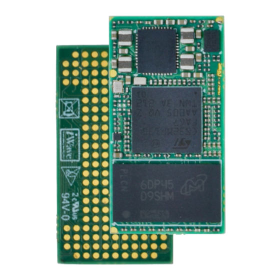
The STM32MP13x OSM LGA Module PCB thickness is 1.2mm±0.1mm, top side maximum height component is 1mm (DDR3L). In bottom side, there are no components available. REL0.1 iWave Systems Technologies Pvt. Ltd. Page 48 of 51 DRAFT VERSION SUBJECT TO CHANGE... -
Page 49: Ordering Information
The below table provides the standard orderable part numbers for different STM32MP13x OSM LGA Module variants. Please contact iWave for orderable part number of higher RAM memory size or Flash memory size Module configurations. Also, if the desired part number is not listed in below table or if any custom configuration part number is required, please contact iWave. -
Page 50: Appendix
5. APPENDIX STM32MP13x OSM Development Platform iWave Systems supports iW-RainboW-G54D-STM32MP13x Development Platform which is targeted for quick validation of STM32MP13 MPU based OSM and its features. Being a OSM of Size-0F form factor with 30mm x 15mm size, the OSM Development Platform is highly useful for testing all the necessary interfaces & also has on-board connectors to validate complete OSM supported features. -
Page 51: Iwave Systems Technologies Pvt. Ltd
STM32MP13x OSM Size-0F LGA Module Hardware User Guide REL0.1 iWave Systems Technologies Pvt. Ltd. Page 51 of 51 DRAFT VERSION SUBJECT TO CHANGE...
Need help?
Do you have a question about the iW-RainboW-G54M STM32MP13 Series and is the answer not in the manual?
Questions and answers