
Related Manuals for Freescale Semiconductor MSC8144ADS


Summary of Contents for Freescale Semiconductor MSC8144ADS
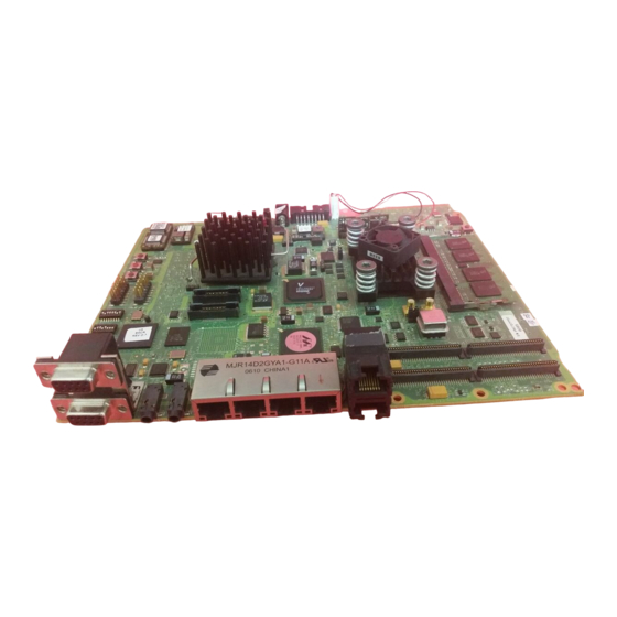
- Page 1 MSC8144ADS Processor Board Reference Manual MSC8144ADSRM Rev 0, February 2007 Downloaded from Elcodis.com electronic components distributor...
- Page 2 Technical Information Center purpose, nor does Freescale Semiconductor assume any liability arising out of the Schatzbogen 7 application or use of any product or circuit, and specifically disclaims any and all 81829 Muenchen, Germany liability, including without limitation consequential or incidental damages.
-
Page 3: Table Of Contents
Chain............1-2 MSC8144ADS processor board Features ......1-2 External Connections . - Page 4 BCSR7 Board Control Register 7 ........5-28 MSC8144ADS Reference Manual, Rev. 0...
- Page 5 AMC in ATCA Environment........6-10 Replacing the MSC8144 DSP MSC8144ADS Reference Manual, Rev. 0 Freescale Semiconductor Downloaded from Elcodis.com...
- Page 6 Contents MSC8144ADS Reference Manual, Rev. 0 Freescale Semiconductor Downloaded from Elcodis.com electronic components distributor...
-
Page 7: General Information
(ADS) that provides a complete debugging environment for engineers developing applications for the Freescale MSC8144 DSP family.The MSC8144ADS processor board is intended to serve as a platform for software and hardware development in the MSC8144 processor environment. On-board resources and the associated... -
Page 8: Standalone Mode
DIP switches (SW[2–3]). 1.1.3.2 Chain A chain connection can be used to debug applications for the MSC8144ADS processor board. In such a case, the debugger can only be connected to the MSC8144-MPC8560 via the P1 connection. Use the DIP switches (SW2.3) to configure the board for this. -
Page 9: External Connections
— Main Power-On Reset (for both Host and Slave); — Hard Reset, Soft Reset, and NMI for MSC8144 1.3 External Connections The MSC8144ADS processor board interconnects with external devices via the following set of connectors (see Figure 1-1 and Figure 1-2): Double RS232 9-pin connector (P2). - Page 10 ISP 14-pin connector to program Altera FPGA. (P3) MSC8144 OnCE Debug connector 14-pin (P1 for single or chain). AMC edge connector (P26) Figure 1-1. MSC8144ADS processor board External Connections (front view) 9 10 Figure 1-2. MSC8144ADS processor board External Connections (rear view) MSC8144ADS Reference Manual, Rev.
-
Page 11: Block Diagram
Diff Signals: SGMII & SRIO E1/T1 LA connector MICTOR RJ48 Framer GETH interfaces sRIO hw switch Framer a. Optional function Mode <number> mean MSC8144 Pinmux Mode Figure 1-3. MSC8144ADS Block Diagram MSC8144ADS Reference Manual, Rev. 0 Freescale Semiconductor Downloaded from Elcodis.com electronic components distributor... -
Page 12: Definitions, Acronyms, And Abbreviations
Reduced Gigabit Media Independent Interface RMII Reduced Media Independent Interface RCW(L,H) Reset Configuration Word (Low/High) Real Time Clock SGMII Serial Gigabit Media Independent Interface SerDes Serializer/Deserializer Type of Mini-RF connector MSC8144ADS Reference Manual, Rev. 0 Freescale Semiconductor Downloaded from Elcodis.com electronic components distributor... -
Page 13: Related Documentation
— MSC8144 Data Sheet — MSC8144 Reference Manual — MSC8144 ADS Processor Board Hardware Getting Started — MSC8144 ADS Using Code Warrior™ and MSC8144ADS Kit Configuration Guide „ Third Party Documentation — PICMG2.15 PCI Telecom Mezzanine/Carrier Card Specification 1.7 Specifications The MSC8144ADS processor board specifications are given in Table 1-2. - Page 14 RS-232 transceiver allows data exchange at 115 Kbps Compliant with standard. Used to control peripheral devices UTOPIA2 8/16-bit UTOPIA level II interfaces for ATM running up to 50 MHz. Acts as a master MSC8144ADS Reference Manual, Rev. 0 Freescale Semiconductor Downloaded from Elcodis.com electronic components distributor...
-
Page 15: Hardware Preparation And Installation
„ Refer to packing list and verify that all items are present. „ Save packing material for storing and reshipping of equipment. 2.2 Installation Instructions To install the MSC8144ADS processor board properly, perform the following steps in the order indicated: Verify that Jumpers and Switches are in default positions (see Chapter 4, Controls and Indicators for a list of default positions). - Page 16 Hardware Preparation and Installation LD1- Figure 2-1. LED Locations The LEDs operate in the following sequences during reset: LD8 and LD1 light LD3 and LD4 light and then go off MSC8144ADS Reference Manual, Rev. 0 Freescale Semiconductor Downloaded from Elcodis.com electronic components distributor...
-
Page 17: Memory Map
Memory Map Each of the processors on the ADS board uses its own memory map. 3.1 MPC8560 Host Mapping for the MSC8144ADS The MPC8560 Memory Controller governs all access to the processor memory slaves. Consequently, the memory map may be reprogrammed according to specific user needs. After performing a Hard Reset sequence, the debug host may initialize the memory controller via the JTAG/COP connector to allow additional access to bus addressable peripherals. -
Page 18: Msc8144 Mapping
FEE00000–FEE3FFFF Packet — Internal 256 Kbyte Processor FEE40000–FEEFFFFF Empty Space — 768 Kbyte FEF00000–FEF17FFF Boot ROM — Internal 96 Kbyte FEF18000–FFFFFFFF — Empty Space — 928 Kbyte MSC8144ADS Reference Manual, Rev. 0 Freescale Semiconductor Downloaded from Elcodis.com electronic components distributor... -
Page 19: Controls And Indicators
Controls and Indicators This chapter describes controls and indicators of the MSC8144ADS processor board, which includes switches, jumpers, LEDs, and push buttons. LD1- Figure 4-1. MSC8144ADS Switches, Jumpers, LEDs, Push Buttons Locations MSC8144ADS Reference Manual, Rev. 0 Freescale Semiconductor Downloaded from Elcodis.com... -
Page 20: Dip Switches
0 Sets PCI as boot port (default) RC12 (works together with SW3.1–SW3.3) for more details and all options, see MSC8144 Reference Manual, under the RCW field Factory setting: '00000110 MSC8144ADS Reference Manual, Rev. 0 Freescale Semiconductor Downloaded from Elcodis.com electronic components distributor... - Page 21 0 Clock_in frequency range is less than or equal 66 MHz (default) — 1 Clock_in frequency is greater than 66 MHz. — SW3.6–SW3.8: Reserved 111 Default Factory setting: ’10010111’ MSC8144ADS Reference Manual, Rev. 0 Freescale Semiconductor Downloaded from Elcodis.com electronic components distributor...
- Page 22 For more details, see MSC8144 Reference Manual, under the RCW field Factory setting: '01000010' Table 4-2. Default Settings (boot from EEPROM) Switch Table 4-3. Default Settings (boot from PCI) Switch MSC8144ADS Reference Manual, Rev. 0 Freescale Semiconductor Downloaded from Elcodis.com electronic components distributor...
-
Page 23: Jumpers
667 MHz CPM & CCB 266 MHz 266 MHz 33 MHz Jumpers Figure 4-1 shows the locations of the jumpers. MSC8144ADS processor board jumpers settings are described in 4-5, below. Table 4-5. Jumpers Jumper Description Soldered jumper. Sets GE interface voltage to 2.5V or 3.3V. -
Page 24: Leds
Controls and Indicators 4.3 LEDs Figure 4-1 shows the locations of the MSC8144ADS processor board LEDs that are described in Table 4-6. Table 4-6. LED Descriptions Name Color LED On LED Off Green Power Good Power Supply fail(*) Green BCSR4.5 is low BCSR4.5 is high... -
Page 25: Ads Functional Description
5.1.2 DDR1 The MSC8144ADS can use two DDR1 SODIMM modules. These have ECC functionality and include 3 or 5 DDR1 parts with a 16- or 8-bit size, respectively. The DDR1 modules each draw 2.6 V from TPS51116 power supply on the MSC8144ADS. -
Page 26: Power For Ddr Devices
VDDQ VTTREF & VTT Memory System 2.6 V /2 = 1.3 V DDR1 VDDQ (GND on SODIMM) 1.8 V /2 = 0.9 V DDR2 VDDQ (NC on SODIMM) MSC8144ADS MSC8144, Rev. 0 Freescale Semiconductor Downloaded from Elcodis.com electronic components distributor... -
Page 27: Mpc8560 Pci Host Bus
MSC8144 port G1 through the GETH phy. This interconnection allows exchanging of data between the host and the MSC8144, and to connect any port out to the LAN. Figure 5-2 shows the GETH interconnection. MSC8144ADS MSC8144, Rev. 0 Freescale Semiconductor Downloaded from Elcodis.com... - Page 28 88E1145 p.p. 1,2 MDX_Addr = 0x13, 0x12 Note: The Host TSEC2 port configured as RGMII is connected to the Quad 88E1145 phy port 0. Figure 5-2. GETH Interconnection Diagram MSC8144ADS MSC8144, Rev. 0 Freescale Semiconductor Downloaded from Elcodis.com electronic components distributor...
-
Page 29: Serial Rapidio Ports
TDM. For each framer (TDM Enable and Reset), there are two sets of control signals: BCSR0[1], BCSR2[4] and BCSR0[2], and BCSR2[5] that allow isolation of the framer outputs. MSC8144ADS MSC8144, Rev. 0 Freescale Semiconductor Downloaded from Elcodis.com... -
Page 30: Tdm Bus Interconnection
Figure 5-3. TDM Scheme A MSC8144 TLV320AIC22 CODEC TDM0TCLK BCLK 24.576MHz MCLK FSYNC TDM0TSYNC +/-100ppm TDM0RDAT DOUT nCODEC_RST RESET TDM0TDAT nCODEC_EN PWRDWN Master Mode Figure 5-4. TDM Scheme B MSC8144ADS MSC8144, Rev. 0 Freescale Semiconductor Downloaded from Elcodis.com electronic components distributor... - Page 31 • DSR = Data Set Ready (I) NC • CTS = Clear To Send (I) NC • RTS = Request To Send (O) NC Stacked DB-9 Figure 5-5. RS-232 Serial Port Connectors MSC8144ADS MSC8144, Rev. 0 Freescale Semiconductor Downloaded from Elcodis.com electronic components distributor...
-
Page 32: C Bus Interconnection
BOOTWP bit BCSR0[4]. Its default value is high, which protects the device against undesirable write operation. Chip Enable pins E0, E1, and E2 are grounded to provide MPC8560 boot function. MSC8144ADS MSC8144, Rev. 0 Freescale Semiconductor Downloaded from Elcodis.com... -
Page 33: Serial Eeprom For Msc8144 Boot
„ Registers 6–10 and 16 are used to control codec 2. „ Registers 11–14 and 17 are used to configure the device inputs, outputs, and clocking. „ Register 21 is used for Device ID and preamp control. MSC8144ADS MSC8144, Rev. 0 Freescale Semiconductor Downloaded from Elcodis.com... -
Page 34: Power Manager
Table 5-5. This feature requires a disable signal on the SPI Select lines driving MPC8560 from the Host ( ). This may be achieved while the Host stays in reset with DIP-switch SW2[1] in the OFF position. MSC8144ADS MSC8144, Rev. 0 5-10 Freescale Semiconductor Downloaded from Elcodis.com... -
Page 35: Reset Operation And Configuration
GPIO20. To enable write operation, configure GPIO20 as an output and to drive the high level. 5.9 Reset Operation and Configuration This section describes overall reset connectivity on the ADS board and how the power-on reset and hard reset sequences function. MSC8144ADS MSC8144, Rev. 0 Freescale Semiconductor 5-11 Downloaded from Elcodis.com... -
Page 36: Reset Connectivity
These initiate values are defined by DIP-switch values latched into the FPGA BCSRs during PORESET and driven towards the appropriate MSC8144 pins until SRESET is deasserted. The RCW[0–16] configuration signals used for Reduced Configuration Word apply the similar way. MSC8144ADS MSC8144, Rev. 0 5-12 Freescale Semiconductor Downloaded from Elcodis.com... -
Page 37: Hard Reset Configuration
Reserved Reserved 21-20 RS_RCS RapidIO/SGMII RCW3. Selects RIO/SGMII reference Reference Clock whether to enable or Clock is 100MHz. Select disable power to the RapidIO and Ethernet blocks. MSC8144ADS MSC8144, Rev. 0 Freescale Semiconductor 5-13 Downloaded from Elcodis.com electronic components distributor... - Page 38 Boot port configured with Boot port configured no Boot Port no SMII SMII (PCI) BPRTC Configuration 27 -26 RCW[15–14]. RCW[15–14] Boot port configuration value 1 and 0. MSC8144ADS MSC8144, Rev. 0 5-14 Freescale Semiconductor Downloaded from Elcodis.com electronic components distributor...
-
Page 39: Clock Options
Figure 5-10. The clock circuits are locked, according to the selected clock mode, when the first stage of the system reset configuration is done (reset configuration is controlled by the RESET block). MSC8144ADS MSC8144, Rev. 0 Freescale Semiconductor 5-15 Downloaded from Elcodis.com... -
Page 40: Shmoo Programmable Clock
The CLK1 output may be connected to the MSC8144 CLKIN pin. The CLK2 output drives variant frequencies to MSC8144 PLL2 (Figure 5-11), which is connected to the PCI_CLK_IN input. Figure 5-11. Programmable Clock Block Diagram MSC8144ADS MSC8144, Rev. 0 5-16 Freescale Semiconductor Downloaded from Elcodis.com... -
Page 41: Jtag Debug Port Connectivity
„ LBC bus; „ 64-bit PCI controller configured in 32-bit mode; „ Two integrated TSEC 1Gbps in RGMII mode. „ CPM SPI port in multi-master mode; „ CPM FCC1 Utopia bus; MSC8144ADS MSC8144, Rev. 0 Freescale Semiconductor 5-17 Downloaded from Elcodis.com... -
Page 42: Host Configuration
CCB/SYSCLK = 4 LALE,LGPL2 cfg_pll_core[0:1] 4.7k Pull-Up/Down Core/CCB = 3 LA27 The e500 core is allowed to boot without waiting 4.7k Pull-Up for configuration by an external master MSC8144ADS MSC8144, Rev. 0 5-18 Freescale Semiconductor Downloaded from Elcodis.com electronic components distributor... -
Page 43: Host Memory Module
Figure 5-13 shows the read timing for the Flash memory. Figure 5-14 shows the signal connections between the Flash memory and the MPC8560 multiplexed local bus. The interface also supports single/page asynchronous and burst synchronous with 16-bit accesses. MSC8144ADS MSC8144, Rev. 0 Freescale Semiconductor 5-19 Downloaded from Elcodis.com... -
Page 44: Ds3 Framer On Lbiu
HRST_REQ output signal or by setting BCSR2[0] = 0. Figure 5-15 shows the read/write timing for the DS3 framer. Figure 5-16 shows the signal connections between the DS3 framer and the MPC8560 Multiplexed Local bus. MSC8144ADS MSC8144, Rev. 0 5-20 Freescale Semiconductor Downloaded from Elcodis.com... -
Page 45: Bcsr On Fpga (Optional)
LBIU in the CS1 Memory Space. The Register File may achieve 32 8-bit slices. CS1 configures as GPCM. Figure 5-17 shows the signal connections between the FPGA and the MPC8560 Multiplexed Local bus. MSC8144ADS MSC8144, Rev. 0 Freescale Semiconductor 5-21 Downloaded from Elcodis.com... -
Page 46: Interrupt Assignment
INTC IRQ4 INTD 4xGETH phy IRQ5 88E1145 IRQ6 IRQ7 DS1374 IRQ8 IRQ9 E1/T1 IRQ10 E1/T1 DS26251 DS26251 INTB INTB XRT79L71 O.D. FPGA Figure 5-18. ADS Interrupt Scheme MSC8144ADS MSC8144, Rev. 0 5-22 Freescale Semiconductor Downloaded from Elcodis.com electronic components distributor... -
Page 47: Board Control And Status Registers (Bcsrs)
Sections of the BCSR slice control registers generally have low active notations. This means that a bit function will be enabled while the bit is zero. When a bit is set to high (or 1) a related function is disabled. The most significant bit is bit 0. MSC8144ADS MSC8144, Rev. 0 Freescale Semiconductor 5-23 Downloaded from Elcodis.com... -
Page 48: Bcsr0 Board Control Register 0
MSC8144 GPIO[0:3] = 4’b1010 code is present. The LED is unlit when in its inactive (default) state (high). During the Reset Configuration sequence the LED indicates the HRESET assertion. MSC8144ADS MSC8144, Rev. 0 5-24 Freescale Semiconductor Downloaded from Elcodis.com... -
Page 49: Bcsr1 Board Control Register 1
5.14.3 BCSR2 Board Control Register 2 On the board, the BCSR2 acts as a control reset register. The BCSR2, which may be read or written at any time, receives its defaults upon Power-On-Reset. All reset signals mentioned MSC8144ADS MSC8144, Rev. 0 Freescale Semiconductor 5-25 Downloaded from Elcodis.com... -
Page 50: Bcsr3 Board Control Register 3
ATT. PRST PRST Power-on-Reset. Writing low will generate PORESET pulse for ‘1’ after MSC8144ADS to re-configure it except the M3 Reset. reset M3PRST M3 Power-on-Reset. Writing low will generate RESET pulse for the ‘1’ after MSC8144 M3 Memory and main PORESET for the whole board.. -
Page 51: Bcsr4 Board Control Register 4
Indication. Low illuminates the appropriate LED “IND”. When high, the LED is dark RSRV4 Reserved ‘11’ Table 5-14. TDM Clock Divider TDMDIV[0–2] Frequency 16 MHz 8 MHz 4 MHz 2 MHz 0,5–7 Disabled MSC8144ADS MSC8144, Rev. 0 Freescale Semiconductor 5-27 Downloaded from Elcodis.com electronic components distributor... -
Page 52: Bcsr5 Board Control Register 5
SW3.1-3.4 CLKRNG Clock-in Range. MSC8144 Configuration pin SW3.5 PHYStoR SGMII Phy Mode. Low configures the GETH Phy in SGMII Mode. High sets the phy in RGMII Mode. MSC8144ADS MSC8144, Rev. 0 5-28 Freescale Semiconductor Downloaded from Elcodis.com electronic components distributor... -
Page 53: Bcsr8 Board Miscellaneous Register 1
Default mode - FA_M3 module is disabled. FA_MODE_ACT FA Module Activation. High with PORESET places FA Module in operation mode. FA_M3_ACT FA_M3 Module Activation. High with PORESET places FA_M3 Module in operation mode. MSC8144ADS MSC8144, Rev. 0 Freescale Semiconductor 5-29 Downloaded from Elcodis.com electronic components distributor... -
Page 54: Bcsr10 Board Status Register 1
C EEPROM failed due to an error. Low indicates normal operation Not Implemented. Table 5-22. PTMC Card Type Assignment PTMC_type[0:1] Description ‘00’ ‘01’ PCI protocol is supported ‘10’ Incapable PCI protocol ‘11’ Disconnected MSC8144ADS MSC8144, Rev. 0 5-30 Freescale Semiconductor Downloaded from Elcodis.com electronic components distributor... -
Page 55: Bcsr12 Board Status Register 3
Table 5-25. Table 5-25. BCSR14 - FA_M3 Data Register (Offset 0xE) DEF on MNEMONIC Function ATT. PRST FA_M3_DATA FA_M3 Data. Data register for FA_M3 operations. MSC8144ADS MSC8144, Rev. 0 Freescale Semiconductor 5-31 Downloaded from Elcodis.com electronic components distributor... -
Page 56: Bcsr15 Reserved
The BCSR19 Register is a status register (read only). The BCSR19 fields are described below in Table 5-29. Table 5-29. BCSR19 Time Stamp 4 (Offset 0x13) MNEMONIC Function Read At TIMEH Firmware Creation Hour. Programmed MSC8144ADS MSC8144, Rev. 0 5-32 Freescale Semiconductor Downloaded from Elcodis.com electronic components distributor... -
Page 57: Bcsr20 Board Status Register 8
ZM7108 are programmable via the I C bus and can be changed by a user at any time during product development and service. Table 5-31 shows the power distribution on the MSC8144ADS, for the MPC8560, and for the MSC8144. MSC8144ADS MSC8144, Rev. 0 Freescale Semiconductor... - Page 58 DDR1 on SODIMM: 2.5 V @ 3 A Fixed LDO5 — POL3 VDDDRH LT1764EQ_2.5 3.3 V DDR1 on SODIMM: VDDDRH/2 Fixed LDO6 — VTT, VREF 1.25 V FAN1655MTF MSC8144ADS MSC8144, Rev. 0 5-34 Freescale Semiconductor Downloaded from Elcodis.com electronic components distributor...
-
Page 59: Interconnection Details
Errors reporting PCI_REQ_B,PCI_GNT_B PCI_REQ0,PCI_GNT0 — PCI_REQ1,PCI_GNT1 To PTMC INT_OUT IRQ1 Interrupt like INTA# PCI_CLK_IN PCI_CLK_IN Clock Distributor, or Clock synthesizer for MSC8144 UTP2-8/16 RxADDR0 PC15(TxAddr[0]) RxADDR1 PC13(TxAddr[1]) MSC8144ADS MSC8144, Rev. 0 Freescale Semiconductor 5-35 Downloaded from Elcodis.com electronic components distributor... - Page 60 RxSOC PA29(TxSOC) RxPRTY PD16(TxPrty) SPI_MISO RxENB PA31(TxEnb) RxCLAV PA30(TxClav) RCLK PC20(CLK12-TxCLK) Driven from PTMC exp. card TxADDR0 PC14(RxAddr[0]) TxADDR1 PC12(RxAddr[1]) TxADDR2 PC6(RxAddr[2]) TxADDR3 PD29(RxAddr[3]) — PD18(RxAddr[4]) SPI_SLK MSC8144ADS MSC8144, Rev. 0 5-36 Freescale Semiconductor Downloaded from Elcodis.com electronic components distributor...
- Page 61 PC31(CLK1-TDMA1RXCLK) TDM0RSYN PA6(A1L1RSYNC) Fxdata3(TDM0TDAT) PA9(A1L1TXD) TDM0TCLK PC30(CLK2-TDMA1TXCLK) TDM0TSYN PA7(A1L1TSYNC) Fxdata4 (TDM1RDAT) PD12(B1L1RXD) TDM1RCLK PC29(CLK3-TDMB1RXCLK) TDM1RSYN PD10(B1L1RSYNC) Fxdata7(TDM1TDAT) PD13(B1L1TXD) TDM1TCLK PC28(CLK4-TDMB1TXCLK) TDM1TSYN PD11(B1L1TSYNC) Fxdata8 (TDM2RDAT) PB14(C1L1RXD) TDM2RCLK PC27(CLK5-TDMC1RXCLK) MSC8144ADS MSC8144, Rev. 0 Freescale Semiconductor 5-37 Downloaded from Elcodis.com electronic components distributor...
- Page 62 PB27(C2L1TXD) TDM6RCLK PB16(CLK18 -TDMC2TXCLK) TDM6RSYN PB25(C2L1TSYNC) Fxdata27(TDM6TDAT) PB26(C2L1RXD) TDM6TCLK PB17(CLK17-TDMC2RXCLK) TDM6TSYN PB24(C2L1RSYNC) Fxdata28 (TDM7RDAT) PB23(D2L1TXD) TDM7RCLK PA2(CLK20 -TDMD2TXCLK) TDM7RSYN PB21(D2L1TSYNC) Fxdata31(TDM7TDAT) PB22(D2L1RXD) TDM7TCLK PA3(CLK19 -TDMD2RXCLK) TDM7TSYN PB20(D2L1RSYNC) MSC8144ADS MSC8144, Rev. 0 5-38 Freescale Semiconductor Downloaded from Elcodis.com electronic components distributor...
- Page 63 MSC8144 TDM[0–3] ports connected directly to appropriated host TDM port, the upper multiplexed ports TDM[4–7] are connected to the host as transmit-to-receive cross. c. Configured as output for testing against the host CPM d. Over FCC2 MPC8560, MSC8144 is configured in Mode 1 MSC8144ADS MSC8144, Rev. 0 Freescale Semiconductor 5-39 Downloaded from Elcodis.com...
- Page 64 ADS Functional Description MSC8144ADS MSC8144, Rev. 0 5-40 Freescale Semiconductor Downloaded from Elcodis.com electronic components distributor...
-
Page 65: Expansion Options
„ The AMC edge connector, with the appropriate connecting device, allows two MSC8144ADS boards to be connected back-to-back, or alternatively, allows an MSC8144ADS to be connected to a TUNDRA device or any other ATCA system. 6.1 PTMC Expansion Card The PTMC expansion card allows expanded ethernet and video connections and serves as a verification tool for the MSC8144ADS. - Page 66 — — +3.3V Power J1-32 AD17 AD17/TDM5TDAT PCI/TDM5 Mode3/Mode2 or Mode0 J1-33 FRAME# FRAME/GE1_RD2/RxDATA4 PCI/GE1-MII/UTP2-16 Mode3/Mode1/Mode0 J1-34 — — J1-35 — — J1-36 IRDY# IRDY/GE1_RD3/RxDATA5 PCI/GE1-MII/UTP2-16 Mode3/Mode1/Mode0 MSC8144ADS Reference Manual, Rev. 0 Freescale Semiconductor Downloaded from Elcodis.com electronic components distributor...
- Page 67 — — — J2-5 — — — J2-6 — — J2-7 — J2-8 RSRV UTP_REOP UTP2-16-POS Mode7 J2-9 RSRV GE1_RX_COL/RxDATA1 GE1MII/UTP2-16 Mode1/Mode0 J2-10 RSRV UTP_TEOP UTP2-16-POS Mode7 MSC8144ADS Reference Manual, Rev. 0 Freescale Semiconductor Downloaded from Elcodis.com electronic components distributor...
- Page 68 — — +3.3V Power J2-42 SERR# SERR/TxDATA0 PCI/UTP2-16 — Pull-Up on ADS J2-43 C/BE1# CBE1/GE1_TX_ER/TxDATA7 PCI/GE1-MII/UTP2-16 Mode3/Mode1/Mode0 J2-44 — — J2-45 AD14 AD14/TDM5RDAT PCI/TDM5 Mode3/Mode2 or Mode0 MSC8144ADS Reference Manual, Rev. 0 Freescale Semiconductor Downloaded from Elcodis.com electronic components distributor...
- Page 69 RMII Mode J3-13 REFCLK GE1_TX_CLK/RxDATA0 GE1/UTP2-16 RMII/SMII Mode J3-14 — — J3-15 — — J3-16 RxD0 GE1_RD0/RxDATA2 GE1/UTP2-16 RMII/SMII Mode J3-17 CT_FA TDM0TSYN TDM0 Main TDM SYNC MSC8144ADS Reference Manual, Rev. 0 Freescale Semiconductor Downloaded from Elcodis.com electronic components distributor...
- Page 70 Any Mode J3-50 CT_D11 TDM2TDAT TDM2 Any Mode J3-51 J3-52 CT_D9 TDM2RSYN TDM2 Any Mode J3-53 CT_D6 TDM1RCLK TDM1 Any Mode J3-54 CT_D7 TDM1TDAT TDM1 Any Mode MSC8144ADS Reference Manual, Rev. 0 Freescale Semiconductor Downloaded from Elcodis.com electronic components distributor...
- Page 71 RxADDR2 UTP2-8/16 Mode3/Mode0 J4-20 J4-21 USER FPGA CTRL2 J4-22 TxENB# RxENB UTP2-8/16 Mode3/Mode0 J4-23 J4-24 RxADR2 TxADDR2 UTP2-8/16 Mode3/Mode0 J4-25 UTP2-8/16 Mode3/Mode0 J4-26 TxCLK RxCLK UTP2-8/16 Mode3/Mode0 MSC8144ADS Reference Manual, Rev. 0 Freescale Semiconductor Downloaded from Elcodis.com electronic components distributor...
- Page 72 USER3 SCL/GPIO26 I/O,O. Pull-Up on ADS J4-58 RxD1 TxDATA9 UTP2-8/16 Mode3/Mode0 J4-59 TxD1 RxDATA9 UTP2-8/16 Mode3/Mode0 J4-60 RxD0 TxDATA8 UTP2-8/16 Mode3/Mode0 J4-61 TxD0 RxDATA8 UTP2-8/16 Mode3/Mode0 J4-62 MSC8144ADS Reference Manual, Rev. 0 Freescale Semiconductor Downloaded from Elcodis.com electronic components distributor...
- Page 73 GE1-MII — — — GE1- RMII — — Test Mode RMII/SMII h/w setting GE2- — GE2-RMII over — — RMII/SMII reserved pins a.Reached with hw production setting MSC8144ADS Reference Manual, Rev. 0 Freescale Semiconductor Downloaded from Elcodis.com electronic components distributor...
-
Page 74: Amc In Atca Environment
The AMC connecting module is shown in Figure 6-1. Fasten the connecting module (by hand) to the AMC edge connector as shown in Figure 6-2. Two MSC8144ADS boards are shown connected to each other via the AMC connecting module in Figure 6-3. - Page 75 50,51 TX7+/- SRIO_TX1+/- 53,54 RX7+/- SRIO_RX1+/- SCL_L — C to ADS MMC (optional) 59,60 TX6+/- SRIO_TX2+/- Muxed with GE1 SGMII on MSC8144ADS 62,63 RX6+/- SRIO_RX2+/- 65,66 TX7+/- SRIO_TX3+/- Muxed with GE2 SGMII on MSC8144ADS 68,69 RX7+/- SRIO_RX3+/- SCA_L — C to ADS MMC...
- Page 76 Fxdata2(TDM0RCLK) RTM34 - ST_D02 RX12+ Fxdata1(TDM0RSYN) RTM35 - ST_D01 RX12- Fxdata0(TDM0RDAT) RTM36 - ST_D00 a. MSC8144 TDM ports is in “Shared Frame,Sync,Clock and Data Link” mode MSC8144ADS Reference Manual, Rev. 0 6-12 Freescale Semiconductor Downloaded from Elcodis.com electronic components distributor...
- Page 77 The Allen wrench is provided in the tool kit. Figure 7-1. Disconnect Fan Figure 7-2. Loosen Allen screws Figure 7-3. Remove Allen Screws Figure 7-4. Remove Heat Sink MSC8144ADS Reference Manual, Rev. 0 Freescale Semiconductor Downloaded from Elcodis.com electronic components distributor...
- Page 78 Figure 7-5. Remove Chip Figure 7-6. Chip Alignment: Correct Alignment Indicator Alignment Indicator Figure 7-7. Chip Alignment: Indicator on Figure 7-8. Chip Alignment: Indicator on Chip Board MSC8144ADS Reference Manual, Rev. 0 Freescale Semiconductor Downloaded from Elcodis.com electronic components distributor...
Need help?
Do you have a question about the MSC8144ADS and is the answer not in the manual?
Questions and answers