Table of Contents
Advertisement
Quick Links
Getting started with the STEVAL-A6983NV1 synchronous step-down switching
Introduction
The
STEVAL-A6983NV1
is based on the
mode architecture in a VQFN package with internal compensation, to minimize design complexity and size. The device is able
to deliver up to 3 A DC to the load.
The
STEVAL-A6983NV1
operates over an input voltage range of 6 to 38 V to provide a regulated 5 V output at a switching
frequency of 400 kHz.
The board can be easily modified to obtain:
•
the preferred switching frequency, modifying the resistor connected to the FSW pin
•
the preferred power-up threshold, modifying the resistors partition
•
the required output voltage, changing the feedback resistors partition
Use the
eDesignSuite
software to configure the
UM3094 - Rev 1 - February 2024
For further information contact your local STMicroelectronics sales office.
regulator evaluation board based on the A6983NQTR
A6983NQTR
synchronous step-down regulator, which implements the peak current
A6983NQTR
and satisfy the specifications.
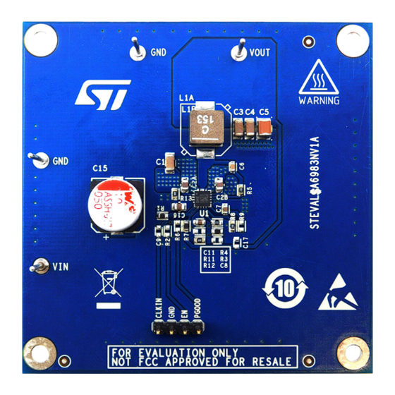
Figure 1.
STEVAL-A6983NV1 evaluation board
UM3094
User manual
www.st.com
Advertisement
Table of Contents

Subscribe to Our Youtube Channel
Related Manuals for ST STEVAL-A6983NV1


Summary of Contents for ST STEVAL-A6983NV1
-
Page 1: Figure 1. Steval-A6983Nv1 Evaluation Board
UM3094 User manual Getting started with the STEVAL-A6983NV1 synchronous step-down switching regulator evaluation board based on the A6983NQTR Introduction STEVAL-A6983NV1 is based on the A6983NQTR synchronous step-down regulator, which implements the peak current mode architecture in a VQFN package with internal compensation, to minimize design complexity and size. The device is able to deliver up to 3 A DC to the load. -
Page 2: Getting Started
Optional spread spectrum for improved EMC • Power good • Synchronization with an external clock • QFN16 (3 x 3 mm) package 1.2.2 Block diagram Figure 2. STEVAL-A6983NV1 functional block diagram VOUT Input Switching Output DC Input LOAD regulator filter filter filter... -
Page 3: Connectors And Test Points
(10%). Otherwise, it is short to the V voltage. 1.2.4 Input EMI filter STEVAL-A6983NV1 is compliant with CISPR16-4-2. The suggested input filters help to reduce EMI. The network consists of a double Pi filter with an inductor (L2), a ferrite bead (L5), MLCC capacitors (C18, C19, C20 and C30), and an electrolytic capacitor used for a bulk energy storage. -
Page 4: Settings
ST products for power conversion applications. You can use it to customize a PFC controller for a specific application. Start by entering the main specifications for your design. Then, generate an automatic design or follow a sequential process to build a highly customized design. -
Page 5: How To Use The Board
UM3094 How to use the board How to use the board STEVAL-A6983NV1 is configured with A6983 LNM with adjustable V . The board is set to deliver a 5 V output voltage with Fsw = 400 KHz. This board is best suited for applications where the low output ripple is preferred on every load condition. -
Page 6: Application 1: Vout = 5 V, Fsw = 400 Khz
• from 6.5 to 38 V • = 5 V • = 0.4 MHz • = 3 A Schematic: Figure 3. STEVAL-A6983NV1 schematic - application 1 Coilcraft: MSS1048 Coilcraft: XAL6060 15uH VOUT VOUT A6983 100nF Ty pe = 50V VIN1... -
Page 7: Oscilloscope Acquisitions For Application 1
UM3094 Application 1: VOUT = 5 V, FSW = 400 KHz Oscilloscope acquisitions for application 1 3.1.1 Power-up from EN • Yellow = EN • Green = inductor current • Blue = V • Violet = V Figure 4. = 6.5 V; V = 5 V;... -
Page 8: Power-Up From Vin
UM3094 Application 1: VOUT = 5 V, FSW = 400 KHz 3.1.2 Power-up from V • Yellow = EN • Green = inductor current • Blue = V • Violet = V Figure 9. = 12 V; V = 5 V; I = 2 A Figure 8. -
Page 9: Vout Ripple For No Load Operation
UM3094 Application 1: VOUT = 5 V, FSW = 400 KHz 3.1.3 ripple for no load operation • Green = inductor current • Blue = V ripple (DC offset = 5 V) • Violet = switching node Figure 12. = 6.5 V; V = 5 V;... -
Page 10: Vout Ripple For Iout = 3 A
UM3094 Application 1: VOUT = 5 V, FSW = 400 KHz 3.1.4 ripple for I = 3 A • Green = inductor current • Blue = V ripple (DC offset = 5 V) • Violet = switching node Figure 16. = 6.5 V;... -
Page 11: Load Transition
UM3094 Application 1: VOUT = 5 V, FSW = 400 KHz 3.1.5 Load transition • from 0.3 to 3 A • = 0.1 A/µs SLOPE • Green = output current • Blue = V ripple (DC offset = 5 V) •... -
Page 12: Performance Curves
UM3094 Application 1: VOUT = 5 V, FSW = 400 KHz 3.1.6 Performance curves Figure 24. Efficiency over I Figure 25. Efficiency over I log scale Vin = 38 [V] Vin = 24 [V] Vin = 12 [V] Vin = 38 [V] Vin = 6.5 [V] Vin = 24 [V] Vin = 12 [V]... -
Page 13: Thermal Acquisitions
UM3094 Application 1: VOUT = 5 V, FSW = 400 KHz Thermal acquisitions The measures have been acquired at the following conditions: 1. T = 25°C 2. I = 3 A The measures have been acquired leaving the device with the reported V and I for more than 5 minutes. -
Page 14: Application 2: Vout = 3.3 V, Fsw = 400 Khz
• from 6.5 to 38 V • = 3.3 V • = 0.4 MHz • = 3 A Schematic: Figure 32. STEVAL-A6983NV1 schematic - application 2 Coilcraft: MSS1048 Coilcraft: XAL6060 8.2uH VOUT VOUT A6983NQTR 100nF Ty pe = 50V VIN1... -
Page 15: Oscilloscope Acquisitions For Application 2
UM3094 Application 2: VOUT = 3.3 V, FSW = 400 KHz Oscilloscope acquisitions for application 2 4.1.1 Power-up from EN • Yellow = EN • Green = inductor current • Blue = V • Violet = V Figure 33. Power-up from EN: V = 6.5 V;... -
Page 16: Power-Up From Vin
UM3094 Application 2: VOUT = 3.3 V, FSW = 400 KHz 4.1.2 Power-up from V • Yellow = EN • Green = inductor current • Blue = V • Violet = V Figure 37. = 6.5 V; V = 3.3 V; I = 3 A Figure 38. -
Page 17: Vout Ripple For No Load Operation
UM3094 Application 2: VOUT = 3.3 V, FSW = 400 KHz 4.1.3 ripple for no load operation • Green = inductor current • Blue = V ripple (DC offset = 3.3 V) • Violet = switching node Figure 41. = 6.5 V; V = 3.3 V;... -
Page 18: Vout Ripple For Iout = 3 A
UM3094 Application 2: VOUT = 3.3 V, FSW = 400 KHz 4.1.4 ripple for I = 3 A • Green = inductor current • Blue = V ripple (DC offset = 3.3 V) • Violet = switching node Figure 45. = 6.5 V;... -
Page 19: Load Transition
UM3094 Application 2: VOUT = 3.3 V, FSW = 400 KHz 4.1.5 Load transition • from 0.3 to 3 A • = 0.1 A/µs SLOPE • Green = output current • Blue = V ripple (DC offset = 5 V) •... -
Page 20: Performance Curves
UM3094 Application 2: VOUT = 3.3 V, FSW = 400 KHz 4.1.6 Performance curves Figure 53. Efficiency over I Figure 54. Efficiency over I log scale Vin = 6.5 [V] Vin = 6.5 [V] Vin = 12[V] Vin = 12 [V] Vin = 24 [V] Vin = 24 [V] Vin = 38 [V]... -
Page 21: Thermal Acquisitions
UM3094 Application 2: VOUT = 3.3 V, FSW = 400 KHz Thermal acquisitions The measures have been acquired at the following conditions: 1. T = 25°C 2. I = 3 A The measures have been acquired leaving the device with the reported V and I for more than 5 minutes. -
Page 22: Application 3: Vout = 3.3 V, Fsw = 2 Mhz
• from 6.5 to 24 V • = 3.3 V • = 2.0 MHz • = 2 A Schematic: Figure 61. STEVAL-A6983NV1 schematic - application 3 Coilcraft: XAL4030 3.3uH VOUT VOUT A6983NQTR 100nF Ty pe = 50V VIN1 VIN2 VINLDO BOOT 0.01K... -
Page 23: Oscilloscope Acquisitions For Application 3
UM3094 Application 3: VOUT = 3.3 V, FSW = 2 MHz Oscilloscope acquisitions for application 3 5.1.1 Power-up from EN • Yellow = EN • Green = output current • Blue = V • Violet = V Figure 62. Power-up from EN: V = 6.5 V;... -
Page 24: Power-Up From Vin
UM3094 Application 3: VOUT = 3.3 V, FSW = 2 MHz 5.1.2 Power-up from V • Yellow = EN • Green = output current • Blue = V • Violet = V Figure 66. = 6.5 V; V = 3.3 V; I = 2 A Figure 67. -
Page 25: Vout
UM3094 Application 3: VOUT = 3.3 V, FSW = 2 MHz 5.1.3 ripple for no load operation • Green = inductor current • Blue = V ripple (DC offset = 3.3 V) • Violet = switching node Figure 70. = 6.5 V; V = 3.3 V;... -
Page 26: Vout Out = 2 A
UM3094 Application 3: VOUT = 3.3 V, FSW = 2 MHz 5.1.4 ripple for I = 2 A • Green = inductor current • Blue = V ripple (DC offset = 3.3 V) • Violet = switching node Figure 74. = 6.5 V;... -
Page 27: Load Transition
UM3094 Application 3: VOUT = 3.3 V, FSW = 2 MHz 5.1.5 Load transition • from 0.3 to 3 A • = 0.1 A/µs SLOPE • Green = inductor current • Blue = V ripple (DC offset = 3.3 V) •... -
Page 28: Performance Curves
UM3094 Application 3: VOUT = 3.3 V, FSW = 2 MHz 5.1.6 Performance curves Figure 82. Efficiency over I Figure 83. Efficiency over I log scale Vin = 6.5 [V] Vin = 6.5 [V] Vin = 12[V] Vin = 12 [V] Vin = 24 [V] Vin = 24 [V] Vin = 38 [V]... -
Page 29: Thermal Acquisitions
UM3094 Application 3: VOUT = 3.3 V, FSW = 2 MHz Thermal acquisitions The measures have been acquired at the following conditions: 1. T = 25°C 2. I = 2 A The measures have been acquired leaving the device with the reported V and I for more than 5 minutes. -
Page 30: Application 4: Vout = 5 V, Fsw = 2 Mhz
• from 6.5 to 24 V • = 5.0 V • = 2.0 MHz • = 2 A Schematic: Figure 90. STEVAL-A6983NV1 schematic - application 4 Coilcraft: XAL4030 3.3uH VOUT VOUT A6983NQTR 100nF Ty pe = 50V VIN1 VIN2 VINLDO BOOT 0.01K... -
Page 31: Oscilloscope Acquisitions For Application 4
UM3094 Application 4: VOUT = 5 V, FSW = 2 MHz Oscilloscope acquisitions for application 4 6.1.1 Power-up from EN • Yellow = EN • Green = output current • Blue = V • Violet = V Figure 91. Power-up from EN: V = 6.5 V;... -
Page 32: Power-Up From Vin
UM3094 Application 4: VOUT = 5 V, FSW = 2 MHz 6.1.2 Power-up from V • Yellow = EN • Green = I current • Blue = V • Violet = V Figure 95. = 6.5 V; V = 5 V; I = 2.5 A Figure 96. -
Page 33: Vout Ripple For No Load Operation
UM3094 Application 4: VOUT = 5 V, FSW = 2 MHz 6.1.3 ripple for no load operation • Green = inductor current • Blue = V ripple (DC offset = 5.0 V) • Violet = switching node Figure 99. = 6.5 V; V = 5 V;... -
Page 34: Vout Out = 2 A
UM3094 Application 4: VOUT = 5 V, FSW = 2 MHz 6.1.4 ripple for I = 2 A • Green = inductor current • Blue = V ripple (DC offset = 5.0 V) • Violet = switching node Figure 103. = 6.5 V;... -
Page 35: Load Transition
UM3094 Application 4: VOUT = 5 V, FSW = 2 MHz 6.1.5 Load transition • from 0.3 to 3 A • = 0.1 A/µs SLOPE • Green = inductor current • Blue = V ripple (DC offset = 5 V) •... -
Page 36: Performance Curves
UM3094 Application 4: VOUT = 5 V, FSW = 2 MHz 6.1.6 Performance curves Figure 111. Efficiency over I Figure 112. Efficiency over I log scale Vin = 6.5 [V] Vin = 6.5 [V] Vin = 8.5[V] Vin = 8.5 [V] Vin = 12 [V] Vin = 12 [V] Vin = 24 [V]... -
Page 37: Thermal Acquisitions
UM3094 Application 4: VOUT = 5 V, FSW = 2 MHz Thermal acquisitions The measures have been acquired at the following conditions: 1. T = 25°C 2. I = 2 A The measures have been acquired leaving the device with the reported V and I for more than 5 minutes. -
Page 38: Pcb Layout
UM3094 PCB layout PCB layout Figure 119. STEVAL-A6983CNV1 evaluation board - PCB layout (top layer) Figure 120. STEVAL-A6983CNV1 evaluation board - PCB layout (bottom layer) UM3094 - Rev 1 page 38/52... -
Page 39: Stack-Up Layers
UM3094 Stack-up layers Stack-up layers Figure 121. STEVAL-A6983CNV1 stack-up layers UM3094 - Rev 1 page 39/52... -
Page 40: Schematic Diagrams
Schematic diagrams Figure 122. STEVAL-A6983NV1 schematic diagrams... -
Page 41: Bill Of Materials
UM3094 Bill of materials Bill of materials Table 2. STEVAL-A6983NV1 bill of materials Item Q.ty Ref. Part/value Description Manufacturer Order code 10µF 50V, 1206 C1, C3, C4, X7R ceramic (3216 metric), CGA5L1X7R1H106K160AC C12, C13, C14 capacitor 50 V, 10 % 1µF 50V,... - Page 42 UM3094 Bill of materials Item Q.ty Ref. Part/value Description Manufacturer Order code 10Ω, 0603(1608 Resistor PANASONIC ERJ-U01F10R0C metric), 0.01 % TP1, TP2, TP3, Single Male Test points ETTINGER 13.14.145 TP4, Header, 1mm DC-DC A6983NQTR, converter buck A6983NQTR 38 V, 3 A regulator UM3094 - Rev 1 page 42/52...
-
Page 43: Board Versions
UM3094 Board versions Board versions Table 3. STEVAL-A6983NV1 versions PCB version Schematic diagrams Bill of materials STEVAL$A6983NV1A STEVAL$A6983NV1A schematic diagrams STEVAL$A6983NV1A bill of materials 1. This code identifies the STEVAL-A6983NV1 evaluation board first version. UM3094 - Rev 1 page 43/52... -
Page 44: Regulatory Compliance Information
UM3094 Regulatory compliance information Regulatory compliance information Notice for US Federal Communication Commission (FCC) For evaluation only; not FCC approved for resale FCC NOTICE - This kit is designed to allow: (1) Product developers to evaluate electronic components, circuitry, or software associated with the kit to determine whether to incorporate such items in a finished product and (2) Software developers to write software applications for use with the end product. -
Page 45: Revision History
UM3094 Revision history Table 4. Document revision history Date Revision Changes 09-Feb-2024 Initial release. UM3094 - Rev 1 page 45/52... -
Page 46: Table Of Contents
UM3094 Contents Contents Getting started ..............2 Safety precautions . - Page 47 UM3094 Contents 5.1.3 ripple for no load operation ......... . . 25 5.1.4 ripple for I = 2 A .
-
Page 48: List Of Tables
STEVAL-A6983NV1 bill of materials ........ -
Page 49: List Of Figures
STEVAL-A6983NV1 schematic - application 2 ........ - Page 50 STEVAL-A6983NV1 schematic - application 3 ........
- Page 51 STEVAL-A6983NV1 schematic diagrams ........
- Page 52 ST’s terms and conditions of sale in place at the time of order acknowledgment. Purchasers are solely responsible for the choice, selection, and use of ST products and ST assumes no liability for application assistance or the design of purchasers’...
Need help?
Do you have a question about the STEVAL-A6983NV1 and is the answer not in the manual?
Questions and answers