Sign In
Upload
Manuals
Brands
ST Manuals
Controller
STEVAL-A6983NV1
ST STEVAL-A6983NV1 Manuals
Manuals and User Guides for ST STEVAL-A6983NV1. We have
1
ST STEVAL-A6983NV1 manual available for free PDF download: Getting Started
ST STEVAL-A6983NV1 Getting Started (52 pages)
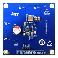
synchronous step-down switching regulator evaluation board based on the A6983NQTR
Brand:
ST
| Category:
Controller
| Size: 15 MB
Table of Contents
Figure 1. STEVAL-A6983NV1 Evaluation Board
1
1 Getting Started
2
Figure 2. STEVAL-A6983NV1 Functional Block Diagram
2
Table 1. Switching Frequency Settings
3
Edesignsuite
4
Settings
4
VOUT Settings
4
Overview
2
Features
2
Block Diagram
2
Safety Precautions
2
Connectors and Test Points
3
Input EMI Filter
3
Switching Frequency Settings
3
2 How to Use the Board
5
Figure 3. STEVAL-A6983NV1 Schematic - Application 1
6
Oscilloscope Acquisitions for Application 1
7
Power-Up from en
7
3 Application 1: VOUT = 5 V, FSW = 400 Khz
6
Figure 23. VIN = 38 V; V out = 5 V; IOUT MAX = 5.149 a
7
Figure 4. VIN = 6.5 V; V out = 5 V; IOUT = 2 a
7
Figure 77. VIN = 24 V
7
Figure 31. VIN = 38 V
7
Figure 33. Power-Up from en
7
Figure 34. Power-Up from en
7
Vin = 24 V
8
Figure 8. VIN = 6.5 V; VOUT = 5 V; IOUT = 2 a
8
Figure 10. VIN = 24 V; VOUT = 5 V; IOUT = 2 a
8
VOUT Ripple for no Load Operation
9
Power-Up from VIN
8
Vin = 12 V
8
Figure 12. VIN = 6.5 V; V out = 5 V; no Load
9
Figure 13. VIN = 12 V; V out out , RIPPLE < 10 MV
9
Figure 46. VIN = 12 V
9
Figure 14. VIN = 24 V; V out out , RIPPLE < 10 MV
9
Figure 44. VIN = 38 V; V out out , RIPPLE < 10 MV
9
Figure 18. VIN = 24 V
10
OUT , RIPPLE < 15 MV
10
Load Transition
11
Figure 48. VIN = 38 V
9
Figure 7. in = 38 V; V out = 5 V; IOUT = 2 a
9
Figure 74. VIN = 6.5 V
9
OUT , RIPPLE < 10 MV
9
VOUT Ripple for IOUT = 3 a
10
Figure 67. VIN = 12 V
11
Figure 20. VIN = 8.5 V
11
Out Min = 4.849 a
11
Figure 22. VIN = 24 V
11
Figure 60. VIN = 38 V
11
Figure 9. in = 12 V; V out = 5 V; IOUT = 2 a
11
Figure 11. in = 38 V; V out = 5 V; IOUT = 2 a
11
Out = 5 V
11
Out Min = 4.853 a
11
Figure 26. Power Losses over IOUT
12
Figure 25. Efficiency over IOUT Log Scale
12
Figure 24. Efficiency over IOUT
12
Figure 27. Load Regulation
12
Performance Curves
12
Thermal Acquisitions
13
Out = 5 V
13
Vin = 24 V; V out = 5 V
13
4 Application 2: VOUT = 3.3 V, FSW = 400 Khz
14
Figure 32. STEVAL-A6983NV1 Schematic - Application 2
14
Figure 58. in = 12 V
15
Figure 15. in = 38 V; V out out , RIPPLE < 10 MV
15
Figure 36. Power-Up from en
15
Figure 37. VIN = 6.5 V; VOUT = 3.3 V; IOUT = 3 a
16
Figure 38. VIN = 12 V; V out = 3.3 V; IOUT = 3 a
16
Figure 39. VIN = 24 V; VOUT = 3.3 V; IOUT = 3 a
16
Figure 40. VIN = 38 V; V out = 3.3 V; IOUT = 3 a
16
Figure 17. in = 12 V
17
Figure 19. in = 38 V
17
Figure 21. VIN = 12 V; V out = 5 V; IOUT MAX = 5.149 A; IOUT MIN = 4.857 a
17
Figure 28. in = 6.5 V
17
Figure 41. VIN = 6.5 V; V out = 3.3 V; no Load
17
Figure 42. VIN = 12 V; V out out , RIPPLE < 10 MV
17
Figure 43. VIN = 24 V; V out out , RIPPLE < 10 MV
17
OUT , RIPPLE < 10 MV
17
Out out
17
VOUT Ripple for no Load Operation
17
Figure 45. VIN = 6.5 V
18
Figure 47. VIN = 24 V
18
OUT , RIPPLE < 10 MV
18
OUT , RIPPLE < 15 MV
18
OUT , RIPPLE < 50 MV
18
OUT , RIPPLE < 8 MV
18
Vout = 3.3 V; Iout
18
VOUT Ripple for IOUT = 3 a
18
Figure 49. VIN = 6.5 V
19
Figure 51. in = 24 V
19
Figure 52. VIN = 38 V; VOUT = 5 V; I
19
Figure 53. Efficiency over IOUT
20
Figure 56. Load Regulation
20
Log Scale
20
Performance Curves
20
Figure 57. VIN = 6.5 V; VOUT
21
Figure 59. VIN = 24 V; VOUT
21
Out = 3.3 V
21
Thermal Acquisitions
21
Figure 61. STEVAL-A6983NV1 Schematic - Application 3
22
Out
22
Oscilloscope Acquisitions for Application 3
23
Power-Up from en
23
In = 12 V
15
In = 24 V
15
In = 6.5 V
15
Out = 3.3 V; Iout = 3 a
15
Figure 50. VIN = 12 V; VOUT = 5 V; I
19
Load Transition
19
Figure 35. Power-Up from en
15
Oscilloscope Acquisitions for Application 2
15
Power-Up from en
15
Power-Up from VIN
16
5 Application 3: VOUT = 3.3 V, FSW = 2 Mhz
22
Figure 94. Power-Up from en
23
Figure 92. Power-Up from en
23
Figure 66. VIN = 6.5 V; VOUT = 3.3 V; I
24
Figure 68. VIN = 15.5 V; VOUT = 3.3 V; I
24
Figure 70. VIN = 6.5 V
25
Figure 71. in = 12 V
25
Figure 72. VIN = 15.5 V
25
Figure 73. VIN = 24 V; VOUT
25
Figure 80. VIN = 15.5 V
25
Figure 87. VIN = 12 V
25
Out = 2 A; Vout
25
V; no Load; VOUT , RIPPLE < 6 MV
25
Vout
25
Figure 76. VIN = 15.5 V
26
Vout out = 2 a
26
Figure 29. in = 12 V
27
Figure 79. VIN = 12 V; VOUT = 3.3 V
27
Figure 81. VIN = 24 V; VOUT = 3.3 V
27
Load Transition
27
Out Max = 3.406 a
27
Out Max = 3.407 a
27
Out Max = 3.426 a
27
Out Min
27
Figure 82. Efficiency over IOUT
28
Figure 83. Efficiency over IOUT
28
Figure 84. Power Losses over IOUT
28
Log Scale
28
Out out
28
Performance Curves
28
Figure 86. VIN = 6.5 V; VOUT
29
Figure 88. VIN = 15.5 V; VOUT
29
Thermal Acquisitions
29
Figure 93. Power-Up from en
23
Figure 69. VIN = 24 V
24
Out = 2 a
24
Power-Up from VIN
24
Figure 91. Power-Up from en
23
Figure 65. Power-Up from en
23
Out = 2 a
23
Out
23
V; Iout = 2 a
23
6 Application 4: VOUT = 5 V, FSW = 2 Mhz
30
Out
30
Oscilloscope Acquisitions for Application 4
31
Power-Up from en
31
V; Vout = 5 V
31
Vout = 5 V
31
Power-Up from VIN
32
Figure 97. VIN = 12 V; VOUT = 5 V; I
32
Figure 95. VIN = 6.5 V; VOUT = 5 V; I
32
Out = 2.5 a
32
Vin = 12 V
33
OUT = 5 V; no Load; VOUT , RIPPLE < 10 MV
33
OUT = 5 V; no Load; VOUT , RIPPLE < 8 MV
33
Vin = 6.5 V
33
VOUT Ripple for no Load Operation
33
RIPPLE < 5 MV
33
OUT = 3.3 V; no Load
33
Vout out = 2 a
34
OUT = 5 V; IOUT = 2 A; VOUT , RIPPLE < 15 MV
34
OUT = 5 V; IOUT = 2 A; VOUT , RIPPLE < 8 MV
34
VOUT , RIPPLE < 10 MV
34
VOUT , RIPPLE < 8 MV
34
Load Transition
35
Figure 98. in = 24 V
35
Out = 5 V; Vout Max = 5.151 A; Vout Min = 4.875 a
35
Out = 5 V; Vout Max = 5.155 A; Vout Min = 4.875 a
35
Out = 5 V; Vout Max = 5.159 A; Vout Min = 4.867 a
35
Efficiency over IOUT Log Scale
36
Power Losses over IOUT
36
In = 8.5 V
37
Vin = 6.5 V
37
Load Regulation
36
Performance Curves
36
Out
36
Figure 115
37
Out = 5 V
37
Thermal Acquisitions
37
Vin = 8.5 V
37
In = 12 V
37
In = 24 V
37
Figure 117
37
7 PCB Layout
38
Figure 119. STEVAL-A6983CNV1 Evaluation Board - PCB Layout (Top Layer)
38
Figure 120. STEVAL-A6983CNV1 Evaluation Board - PCB Layout (Bottom Layer)
38
8 Stack-Up Layers
39
Figure 121. STEVAL-A6983CNV1 Stack-Up Layers
39
9 Schematic Diagrams
40
Figure 122. STEVAL-A6983NV1 Schematic Diagrams
40
Table 2. STEVAL-A6983NV1 Bill of Materials
41
10 Bill of Materials
41
Table 3. STEVAL-A6983NV1 Versions
43
11 Board Versions
43
12 Regulatory Compliance Information
44
Table 4. Document Revision History
45
Table of Contents
46
Revision History
45
List of Tables
48
List of Figures
49
Advertisement
Advertisement
Related Products
ST STEVAL-ESC002V1
ST STEVAL-IHM037V1
ST STEVAL-IAS001V1
ST STEVAL-TTM007A
ST ST5-Q
ST ST5-IP-E
ST STM8AF6268
ST STM32F103 series
ST ST7735R
ST Sitronix ST7038
ST Categories
Motherboard
Computer Hardware
Microcontrollers
Control Unit
Controller
More ST Manuals
Login
Sign In
OR
Sign in with Facebook
Sign in with Google
Upload manual
Upload from disk
Upload from URL