Table of Contents
Advertisement
Quick Links
Advertisement
Table of Contents

Related Manuals for Advantech EWM-W179M201E


Summary of Contents for Advantech EWM-W179M201E
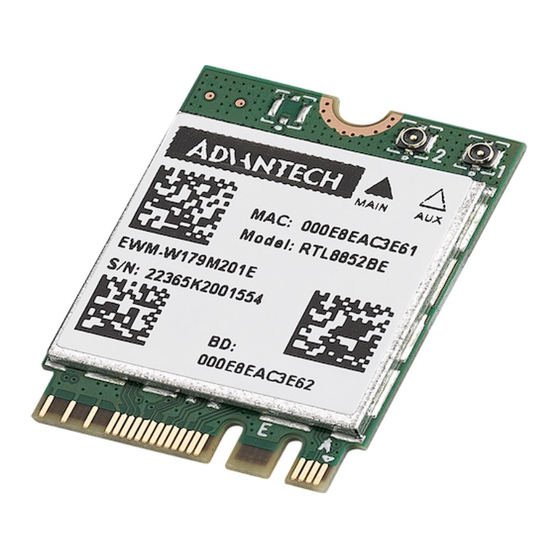
- Page 1 EWM-W179M201E User manual...
-
Page 2: Applicability Type
Applicability Type AIW PN Description WNFT- 802.11ax/ac/b/g/n M.2 2230 Key A/E solution based EWM-W179M201E 238AX(BT) on RTL8852BE chipset... -
Page 3: Revision History
Revision History Version Owner Date Description V1.0 Joejohn.Chen 2023-04-20 First issue V1.1 Joejohn.Chen 2023-06-12 Add Linux /Android Support... -
Page 4: Product Introduction
1 Product Introduction Item Description IEEE 802.11ax/ac/a/b/g/n (2T2R) Standard Bluetooth V5.0, 4.2, V4.1, V4.0LE, V3.0, V2.1+EDR Chipset solution Realtek RTL8852BE 802.11b: 11Mbps 802.11a/g: 54Mbps 802.11n: MCS0~15 Data Rate 802.11ac: MCS0~9 802.11ax: HE0~11 Bluetooth: 1 Mbps, 2Mbps and Up to 3Mbps IEEE 802.11ax/ac/a/b/g/n Operating Frequency ISM Band, 2.412GHz~2.484GHz, 5.150GHz~5.850GHz... - Page 5 Item Description 802.11a: OFDM (BPSK, QPSK, 16-QAM, 64-QAM) 802.11ac: OFDM (BPSK, QPSK, 16-QAM, 64-QAM, 256- QAM) 802.11ax: OFDMA (BPSK, QPSK, 16-QAM, 64-QAM, 256- QAM, 1024-QAM) Modulation Header: GFSK Payload 2M: π/4-DQPSK Payload 3M: 8-DPSK TX mode: 860 mA (Max) Power Consumption RX mode: 450 mA Operating Voltage DC 3.3V...
- Page 6 2 Output Power & Sensitivity 2.1 Wi-Fi 802.11b Data Rate Tx ± 2dBm Rx Sensitivity ≦-76dBm 11Mbps 19dBm 802.11g Data Rate Tx ± 2dBm Rx Sensitivity ≦-65dBm 54Mbps 18dBm 802.11n / 2.4GHz Tx ± 2dBm Tx ± 2dBm Data Rate Rx Sensitivity (1TX) (2TX)
- Page 7 802.11ac Tx ± 2dBm Tx ± 2dBm Data Rate Rx Sensitivity (1TX) (2TX) VHT80 ≦-51dBm MCS9 15dBm 18dBm 802.11ax / 2.4 GHz Tx ± 2dBm Tx ± 2dBm Data Rate Rx Sensitivity (1TX) (2TX) HE40 ≦-49dBm MCS11 13dBm 16dBm 802.11ax / 5 GHz Tx ±...
-
Page 8: Hardware Specification
3 Hardware Specification 3.1 Mechanical Dimension Dimension (L x W x H): 30 mm (Tolerance:±0.15mm) x 22 mm (Tolerance:±0.15mm) x 2.24 mm (Tolerance:±0.3mm) Figure 3-1: Hardware Dimension... -
Page 9: Mhf4 Connector Spec
3.2 MHF4 connector spec Figure 3-2: MHF4 connector spec... -
Page 10: Block Diagram
3.3 Block Diagram Figure 3-3: Block Diagram... -
Page 11: Pin Assignment
3.4 Pin Assignment The following section illustrate signal pin-outs for the module connector. l Top Side Pin Name Type Description Ground connections USB_D+ USB serial differential data Positive USB_D- USB serial differential data Negative Ground connections NOTCH FOR KEY A No Connection NOTCH FOR KEY A No Connection... - Page 12 Pin Name Type Description Ground connections PETp0 PCI Express transmit data- Positive PETn0 PCI Express transmit data- Negative Ground connections REFCLKp0 PCI Express differential clock input- Positive REFCLKn0 PCI Express differential clock input- Negative Ground connections CLKREQ0# PCIe clock request PEWAKE0# PCIe wake signal Ground connections...
-
Page 13: Bottom Side
l Bottom Side Pin Name Type Description 3.3V VDD system power supply input 3.3V VDD system power supply input LED_1# O/OD WLAN LED NOTCH FOR KEY A No Connection NOTCH FOR KEY A No Connection NOTCH FOR KEY A No Connection NOTCH FOR KEY A No Connection LED_2#... - Page 14 Pin Name Type Description COEX3 Do Not Connect COEX_TXD Do Not Connect COEX_RXD Do Not Connect SUSCLK 32.768KHz CLOCK INPUT PERST0# PCIe host indication to reset the device Active low W_DISABLE2# Turn off BT RF analog and front-end. Active low W_DISABLE1# Turn off WLAN RF analog and front-end.
Need help?
Do you have a question about the EWM-W179M201E and is the answer not in the manual?
Questions and answers