Table of Contents
Advertisement
Quick Links
UM_2307_PL88_2308_013018
XDP710 evaluation PCBA user guide
Scope and purpose
Setup and evaluation of XP710 printed circuit board assembly (PCBA).
Intended audience
Test engineers.
Table of contents
Table of contents ............................................................................................................................ 1
1
Introduction .......................................................................................................................... 2
2
Hardware and software requirements ...................................................................................... 2
3
XDP710 evaluation platform .................................................................................................... 3
3.1
Electrical specifications .......................................................................................................................... 3
3.2
Block diagram .......................................................................................................................................... 3
3.3
XDP710 evaluation board schematics .................................................................................................... 5
3.4
XDP710 evaluation board layout ............................................................................................................ 7
3.5
XDP710 evaluation board bill of materials ........................................................................................... 12
3.6
XDP710 evaluation board default settings ........................................................................................... 14
3.7
.......................................................................................................................................................... 16
3.8
FET board ............................................................................................................................................... 16
3.8.1
Different FET footprint options on FET board ...................................................................................... 16
3.9
XDP710 dongle schematics ................................................................................................................... 18
4
Programming, setup, and turn-on instructions ......................................................................... 18
4.1
XDP Designer communication setup .................................................................................................... 19
4.1.1
Check the dongle connection in XDP Designer ............................................................................... 19
4.1.2
Detecting XDP710-002 ...................................................................................................................... 20
4.1.3
Reading and writing registers .......................................................................................................... 22
4.1.4
Program FET ..................................................................................................................................... 23
4.1.5
4.1.6
Watchdog timer selection ................................................................................................................ 24
4.1.7
Program current sense range (CS_RNG) and start-up current limit (IST) ...................................... 25
4.1.8
Program VIN_UV_FAULT_LIMIT ....................................................................................................... 25
4.1.9
Program VIN_OV_FAULT_LIMIT ....................................................................................................... 26
4.1.10
Program VOUT_UV_FAULT_LIMIT ................................................................................................... 26
4.2
XDP710 programming under different modes ..................................................................................... 27
4.2.1
FDM ................................................................................................................................................... 27
4.2.1.1
FDM (DCM) ........................................................................................................................................ 27
4.2.1.2
FDM (ACM)......................................................................................................................................... 28
4.2.2
AADM ................................................................................................................................................. 28
5
Loading configuration file ...................................................................................................... 30
6
Hands-on.............................................................................................................................. 32
6.1
Example test: UV fault ........................................................................................................................... 32
6.2
Programming SOA, OTP, and MTP ........................................................................................................ 33
Revision history............................................................................................................................. 35
User Guide
www.infineon.com/xdp710-001
...................................................................................................................................... 24
sns
Please read the sections "Important notice" and "Warnings" at the end of this
document
V 1.0
2023-08-11
Advertisement
Table of Contents

Related Manuals for Infineon XDP710


Summary of Contents for Infineon XDP710
-
Page 1: Table Of Contents
Electrical specifications .......................... 3 Block diagram ............................3 XDP710 evaluation board schematics ....................5 XDP710 evaluation board layout ......................7 XDP710 evaluation board bill of materials ................... 12 XDP710 evaluation board default settings ................... 14 ................................16 FET board ............................... 16 3.8.1... -
Page 2: Introduction
PMBus communication interface to access their register map in order to configure all of their features. The XDP710 series dongle is a PC-USB COM port to PMBus bridge dongle that allows access to the XDP710 registers from the PC software configurator. This document describes how to set up and use the whole interface for testing purposes, using the Add-Ins menu to format your document. -
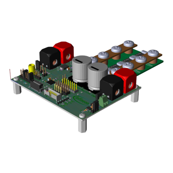
Page 3: Xdp710 Evaluation Platform
Block diagram The XDP710 evaluation platform consists of: XDP710 evaluation board: Positive input hot-swap controller and e-fuse circuitry designed to run a single • channel controller including its corresponding FET. Communication, control and protection circuitry is also included. - Page 4 XDP710 evaluation PCBA user guide XDP710 evaluation platform Figure 4 XDP710 evaluation platform block diagram User Guide V 1.0 2023-08-11...
-
Page 5: Xdp710 Evaluation Board Schematics
XDP710 evaluation PCBA user guide XDP710 evaluation platform XDP710 evaluation board schematics Figure 5 Schematic for main IC User Guide V 1.0 2023-08-11... - Page 6 XDP710 evaluation PCBA user guide XDP710 evaluation platform Figure 6 Schematic for main PCBA ports Figure 7 Schematic for MOSFET PCBA User Guide V 1.0 2023-08-11...
-
Page 7: Xdp710 Evaluation Board Layout
XDP710 evaluation PCBA user guide XDP710 evaluation platform XDP710 evaluation board layout Figure 8 Top layer layout of main PCB User Guide V 1.0 2023-08-11... - Page 8 XDP710 evaluation PCBA user guide XDP710 evaluation platform Figure 9 Mid 1 layer layout of main PCB User Guide V 1.0 2023-08-11...
- Page 9 XDP710 evaluation PCBA user guide XDP710 evaluation platform Figure 10 Mid 2 layer layout of main PCB User Guide V 1.0 2023-08-11...
- Page 10 XDP710 evaluation PCBA user guide XDP710 evaluation platform Figure 11 Bottom layer layout of main PCB User Guide V 1.0 2023-08-11...
- Page 11 XDP710 evaluation PCBA user guide XDP710 evaluation platform Figure 12 Top, Mid 1, Mid 2 and bottom layer layouts of MOSFET PCB User Guide V 1.0 2023-08-11...
-
Page 12: Xdp710 Evaluation Board Bill Of Materials
XDP710 evaluation PCBA user guide XDP710 evaluation platform XDP710 evaluation board bill of materials Table 1 Bill of materials (BOM) for the main PCBA Reference Item Qty Value Characteristics Manufacturer Part number designator Cin, Ci 0.1 µF 200 V X7R... - Page 13 XDP710 evaluation PCBA user guide XDP710 evaluation platform Reference Item Qty Value Characteristics Manufacturer Part number designator R4, R5, R6, R16, R19, 4.7k Panasonic ERJ-3EKF4701V R20, R45 Panasonic ERJ-3EKF10R0V 121k Vishay CRCW0805121KFK 4.71k Yageo RC0603FR-074K7L 12 R11, R12, R13, R35,...
-
Page 14: Xdp710 Evaluation Board Default Settings
XDP710 evaluation PCBA user guide XDP710 evaluation platform Reference Item Qty Value Characteristics Manufacturer Part number designator 28 X29, X31, X32, X34, SMD loop Harwin S2761-46R X36, X37, X38, X39, X42, X43, X46, X47, X48, X49, X50, X51, X52, X53, X54, X55,... - Page 15 XDP710 evaluation PCBA user guide XDP710 evaluation platform Between Pin 5 and 6 and in ADDRx pins configuration to 0x10. Move the jumpers to change between Pins 11 and 12 the PMBus address. MODEx pins configuration. Leave them open for fully digital Open mode (FDM).
-
Page 16: R Sns
XDP710 evaluation PCBA user guide XDP710 evaluation platform Three different footprints are provided to support different resistor sizes. The current onboard resistor is 1 mΩ. There are optional footprints that are optimized for resistor packages on board: : 5930, 5931... - Page 17 XDP710 evaluation PCBA user guide XDP710 evaluation platform Figure 15 SS08 position (bottom side) Figure 16 PG-TSON-8-3 position (bottom side) User Guide V 1.0 2023-08-11...
-
Page 18: Xdp710 Dongle Schematics
• XDP710 powers up as soon as VDD_VIN is equal to or greater than 5.5 V. At this point, communication and programming is possible, but the FET will still be off. To turn on the FET, a minimum of 9 V is required, then the following registers must be programmed at a minimum to turn on the device: •... -
Page 19: Xdp Designer Communication Setup
XDP710 evaluation PCBA user guide Programming, setup, and turn-on instructions Figure 18 XDP710 evaluation board and dongle setup XDP Designer communication setup The following steps explain how to configure and test the evaluation board and dongle using the XDP Designer software. -
Page 20: Detecting Xdp710-002
XDP710 evaluation PCBA user guide Programming, setup, and turn-on instructions Figure 19 USB007A1 detection on XDP Designer 4.1.2 Detecting XDP710-002 Click on the button shown in the red box in Figure 20 and then wait for few seconds; the device should be detected by the GUI automatically. - Page 21 XDP710 evaluation PCBA user guide Programming, setup, and turn-on instructions Figure 21 “Scan For Devices” to find XDP710-002 The detected device will be XDP710V002, with the telemetry displayed on the left side as shown in Figure Figure 22 Live telemetry of connected XDP710-002 User Guide V 1.0...
-
Page 22: Reading And Writing Registers
PMBus registers and the stored values in it, as shown in Figure Figure 23 XDP Designer showing all the PMBus registers of connected XDP710-002 4.1.3 Reading and writing registers For editing any register individually, click on the corresponding PMBus register, make the necessary changes and then click on “Write”... -
Page 23: Program Fet
XDP710 evaluation PCBA user guide Programming, setup, and turn-on instructions Most of the registers are updated automatically, but to read the latest values click on “Read” to read the corresponding register, as shown in Figure Figure 25 Reading VIN_OV_WARN_LIMIT 4.1.4 Program FET If using analog-assisted digital mode (AADM), the FET will be pre-programmed, and this step can be skipped. -
Page 24: Program R
XDP710 evaluation PCBA user guide Programming, setup, and turn-on instructions 4.1.5 Program R The sense resistor value must be programmed in the R bits of the REG_CFG register according to the one populated on the board. The board has R “1mΩ”... -
Page 25: Program Current Sense Range (Cs_Rng) And Start-Up Current Limit (Ist)
XDP710 evaluation PCBA user guide Programming, setup, and turn-on instructions 4.1.7 Program current sense range (CS_RNG) and start-up current limit (IST) If using AADM or analog comparator mode (ACM), this step can be skipped, as the resistor on the IST pin selects the start-up current limit and current sense range. -
Page 26: Program Vin_Ov_Fault_Limit
XDP710 evaluation PCBA user guide Programming, setup, and turn-on instructions 4.1.9 Program VIN_OV_FAULT_LIMIT If using AADM or ACM, this step can be skipped, as the input overvoltage (OV) fault limit is set by external resistors on the OV pin. In DCM, program the desired UV fault limit in the VIN_OV_FAULT_LIMIT register (0x55). If OV fault is not used, the register can be programmed to 88 V, or the fault can be disabled. -
Page 27: Xdp710 Programming Under Different Modes
XDP710 programming under different modes There are two different modes in which the XDP710 can be operated, namely FDM and AADM. FDM has two selections: DCM and ACM. AADM or FDM can be selected based on the resistor connected on the Mode 0 and Mode 1 pins on the evaluation board. -
Page 28: Fdm (Acm)
XDP710 evaluation PCBA user guide Programming, setup, and turn-on instructions Figure 33 Enabling FET by toggling enable signal high 4.2.1.2 FDM (ACM) If the device is to be programmed using ACM, first the ACM need to be selected in register 0xD1, then modify Bit 7 to “0”. - Page 29 XDP710 evaluation PCBA user guide Programming, setup, and turn-on instructions Connector Jumper position (resistor) Function Between 9 and 10 (Mode 1: 20 kΩ (2.0 V)) X21 (IST pins) Between 7 and 8 recommended 25 mV current sense range is (IST: 15 kΩ (1.5 V)) selected and 12.5 percent of...
-
Page 30: Loading Configuration File
XDP710 evaluation PCBA user guide Loading configuration file Loading configuration file This setion describes how the configuration file can be loaded directly into the device, eliminating the need to manually modify the required register. The configuration file can be loaded into the device as follows: •... - Page 31 XDP710 evaluation PCBA user guide Loading configuration file Figure 36 Click on “Load” to load the selected configuration file An example configuration file in .txt format can be found in Figure 37. This configuration file is compatible with the evaluation board in the default configuration.
-
Page 32: Hands-On
XDP710 evaluation PCBA user guide Hands-on Hands-on Example test: UV fault 1. Turn on XDP710 and FET as specified in the previous section for FDM (DCM). 2. Write 38 V to VIN_UV_FAULT_LIMIT register, as shown in Figure Figure 38 Write 38 V to VIN_UV_FAULT_LIMIT 3. -
Page 33: Programming Soa, Otp, And Mtp
Set the input voltage back to 48 V. The fault must be cleared, the FET must be turned back on and the PWRGD LED must turn on again. Programming SOA, OTP, and MTP As specified in the XDP710 datasheet, to program the desired settings in internal commands or OTP at power- up, the following steps must be followed: •... - Page 34 XDP710 evaluation PCBA user guide Hands-on Figure 40 Programming tab 3. Set the program from “Registers”, select the memory section that needs to be programmed and then click on “Program to OTP”, as shown in Figure Figure 41 OTP and MTP programming 4.
-
Page 35: Revision History
XDP710 evaluation PCBA user guide Revision history Revision history Document Date of release Description of changes version V 1.0 2023-08-11 Initial release User Guide V 1.0 2023-08-11... - Page 36 With respect to any examples, hints or any typical 81726 München, Germany values stated herein and/or any information WARNINGS regarding the application of the product, Infineon Technologies hereby disclaims any and all Due to technical requirements products may contain warranties and liabilities of any kind, including dangerous substances.
Need help?
Do you have a question about the XDP710 and is the answer not in the manual?
Questions and answers