Table of Contents
Advertisement
Quick Links
UM012553
XDP™ XDP700-002 evaluation PCBA user guide
About this document
Scope and purpose
This document describes how to set up the XDP™ XDP700-002 Evaluation Board and configure the internal
registers to evaluate the performance of the XDP700-002 hot-swap controller for negative rail.
Intended audience
This document is intended for test engineers who want to evaluate the performance of the XDP700-002
hot-swap controller.
User manual
Please read the sections "Important notice" and "Warnings" at the end of this document
V 1.0
www.infineon.com
2024-04-12
Advertisement
Table of Contents

Related Manuals for Infineon XDP XDP700-002


Summary of Contents for Infineon XDP XDP700-002
-
Page 1: About This Document
Intended audience This document is intended for test engineers who want to evaluate the performance of the XDP700-002 hot-swap controller. User manual Please read the sections “Important notice” and “Warnings” at the end of this document V 1.0 www.infineon.com 2024-04-12... -
Page 2: Important Notice
Boards provided by Infineon Technologies. The design of the Evaluation Boards and Reference Boards has been tested by Infineon Technologies only as described in this document. The design is not qualified in terms of safety requirements, manufacturing, and operation over the entire operating temperature range or lifetime. -
Page 3: Safety Precautions
XDP™ XDP700-002 evaluation PCBA user guide Safety precautions Safety precautions Note: Please note the following warnings regarding the hazards associated with development systems. Table 1 Safety precautions Warning: The evaluation or reference board contains DC bus capacitors which take time to discharge after removal of the main supply. Before working on the drive system, wait five minutes for capacitors to discharge to safe voltage levels. -
Page 4: Table Of Contents
XDP™ XDP700-002 evaluation PCBA user guide Table of contents Table of contents About this document ........................1 Important notice ..........................2 Safety precautions .......................... 3 Table of contents ..........................4 Introduction .......................... 5 Hardware and software requirements ..................6 XDP700-002 evaluation platform ..................... 8 Electrical specifications .......................... -
Page 5: Introduction
Introduction Introduction Infineon’s XDP™ XDP7x0-002 family of devices (XDP700-002, XDP710-002) are highly integrated wide-input voltage system monitoring and inrush current protection devices. These are digitally configurable and use a power management bus (PMBus) communication interface to access their register map to configure their features. -
Page 6: Hardware And Software Requirements
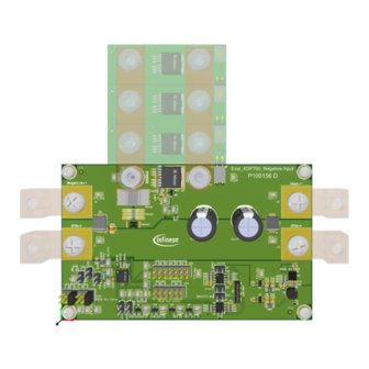
Order code: EVAL_XDP700 − XDP™ Designer USB dongle USB007 or higher • Order code: USB007A1 − XDP™ Designer GUI • Download from Infineon Development Center − Figure 1 XDP700-002 Evaluation Board Figure 2 USB007A1 dongle User manual V 1.0 2024-04-12... - Page 7 XDP™ XDP700-002 evaluation PCBA user guide Hardware and software requirements Figure 3 XDP™ Designer User manual V 1.0 2024-04-12...
-
Page 8: Xdp700-002 Evaluation Platform
XDP™ XDP700-002 evaluation PCBA user guide XDP700-002 evaluation platform XDP700-002 evaluation platform The following sections describe the XDP700-002 Evaluation Board highlighting the electrical specifications, block diagram, schematics, layout, bill of materials (BOM), and different configuration settings that could be used on this evaluation board. Electrical specifications Input and output voltage range: –12 V DC to –80 V DC •... -
Page 9: Xdp700-002 Evaluation Board Schematics
XDP™ XDP700-002 evaluation PCBA user guide XDP700-002 evaluation platform XDP700-002 Evaluation Board schematics Figure 5 Main IC and bias Figure 6 Communication and isolation User manual V 1.0 2024-04-12... - Page 10 XDP™ XDP700-002 evaluation PCBA user guide XDP700-002 evaluation platform Figure 7 MOSFET Figure 8 Configuration selection User manual V 1.0 2024-04-12...
-
Page 11: Xdp700-002 Evaluation Board Layout
XDP™ XDP700-002 evaluation PCBA user guide XDP700-002 evaluation platform Figure 9 MOSFET PCBA XDP700-002 Evaluation Board layout Figure 10 Top layer layout of main PCB User manual V 1.0 2024-04-12... - Page 12 XDP™ XDP700-002 evaluation PCBA user guide XDP700-002 evaluation platform Figure 11 Mid 1 layer layout of main PCB Figure 12 Mid 2 layer layout of main PCB User manual V 1.0 2024-04-12...
- Page 13 XDP™ XDP700-002 evaluation PCBA user guide XDP700-002 evaluation platform Figure 13 Bottom layer layout of main PCB Figure 14 Top, Mid 1, Mid 2, and bottom layer layouts of MOSFET PCB User manual V 1.0 2024-04-12...
-
Page 14: Xdp700-002 Evaluation Board Bill Of Materials
XDP™ XDP700-002 evaluation PCBA user guide XDP700-002 evaluation platform XDP700-002 Evaluation Board bill of materials Table 2 Bill of materials (BOM) for the main PCBA Item Qty Reference designator Value Footprint Manufacturer Part number BRD1 PC Board – – P100156 D (FAB) C1, C2, C3, C4, C9, C21, 0.1 uF... - Page 15 XDP™ XDP700-002 evaluation PCBA user guide XDP700-002 evaluation platform Item Qty Reference designator Value Footprint Manufacturer Part number Q1, Q2, Q3 BSR315P SOT23 Infineon BSR315P Technologies 2N7002E sot23 2N7002ET1G MMBT3904 Sot23 Nexperia MMBT3904,2 IPB017N10N5 PG-TO263-7 Infineon IPB017N10N5 Technologies ATMA1 R1, R2, R5, R6 1.5K...
- Page 16 5930K-1L00F Rsns2 3920 Bourns Not Used Rsns3 0.5uR 2512 Bourns Not Used 220uH LPD5030V Coilcraft LPD5030V- 224MRC ISO1641B ISO1641BDR 2DIB1410F Infineon 2DIB1410FXU LM5018SD/NO WSON-8 Texas LM5018SD/N Instruments U4, U5 3.3 V SOT23-5 STMicroelectron LDK320AM33 XDP700-002 IFX-PG-VQFN- Infineon XDP700-002 29-1 Technologies...
- Page 17 S1, S2, S3, S4 mtg_hole_125 Keystone 2203 40x1/2 C7, C8 C0603 Not used C24a, C25a CAP18X46mm Nichicon Not used DO-219AC Vishay Not used Infineon PG-HSOF-8-1 Not used Technologies PG-HSOG-8-1 Infineon Not used Technologies PG-HDSOP-16 Infineon Not used Technologies PG-TDSON-8_1 Infineon Not used...
-
Page 18: Xdp700-002 Evaluation Board Default Settings
XDP™ XDP700-002 evaluation PCBA user guide XDP700-002 evaluation platform Item Qty Reference designator Value Footprint Manufacturer Part number P710 CON2_RA_TSW- Samtec Not used 102-08-F-S-RA Infineon PG-HSOF-8-1 Not used Technologies PG-HSOG-8-1 Infineon Not used Technologies Infineon PG-HDSOP-16 Not used Technologies PG-TDSON-8_1... -
Page 19: Current Sensing Resistor (R )
XDP™ XDP700-002 evaluation PCBA user guide XDP700-002 evaluation platform Table 5 Resistors and capacitors Reference Default configuration Notes designator Check depending on FET – C7, C8 and C of FET R37, R41 Check depending on sense Can be populated: 10 Ω resistor Max 100 nF filter... - Page 20 XDP™ XDP700-002 evaluation PCBA user guide XDP700-002 evaluation platform Figure 16 TOLL position (top side) Figure 17 PG-TDSON-8-1 position (top side) Figure 18 PG-HDSOP-16 position (bottom side) User manual V 1.0 2024-04-12...
-
Page 21: Usb007A Dongle Schematics
XDP™ XDP700-002 evaluation PCBA user guide XDP700-002 evaluation platform Figure 19 PG-HSOG-8-1 position (bottom side) 3.10 USB007A dongle schematics Figure 20 USB007A1 dongle schematic User manual V 1.0 2024-04-12... -
Page 22: Programming, Setup, And Turn-On Instructions
XDP™ XDP700-002 evaluation PCBA user guide Programming, setup, and turn-on instructions Programming, setup, and turn-on instructions Set up the system as follows: 1. Connect the USB007 dongle to the XDP700-002 Evaluation Board connector X6 as shown in Figure 2. Connect the USB007 dongle to the PC USB port. 3. -
Page 23: Xdp™ Designer Communication Setup
XDP™ XDP700-002 evaluation PCBA user guide Programming, setup, and turn-on instructions XDP™ Designer communication setup Install XDP™ Designer from the Infineon Development Center. 4.1.1 Dongle connection in XDP™ Designer 1. Open XDP™ Designer. 2. Wait for a few moments and check the bottom status bar for the dongle connection. -
Page 24: Detecting Xdp700-002
XDP™ XDP700-002 evaluation PCBA user guide Programming, setup, and turn-on instructions 4.1.2 Detecting XDP700-002 1. Click the button highlighted in Figure 23 and then wait for a few seconds to detect the device. If the device is not detected on its own, click on Scan For Devices, as shown in Figure Figure 23 XDP700-002 detection... - Page 25 XDP™ XDP700-002 evaluation PCBA user guide Programming, setup, and turn-on instructions Figure 25 Live telemetry of the connected XDP700-002 2. Click the PMB button to view PMBus registers and their stored values. See Figure Figure 26 XDP™ Designer displaying PMBus registers of connected XDP700-002 User manual V 1.0 2024-04-12...
-
Page 26: Reading And Writing Registers
XDP™ XDP700-002 evaluation PCBA user guide Programming, setup, and turn-on instructions 4.1.3 Reading and writing registers 1. To edit a register individually, click on the corresponding PMBus register. 2. Make the necessary changes, and then click Write. See Figure Figure 27 Editing VIN_OV_FAULT_LIMIT Most of the registers are updated automatically. -
Page 27: Programming The Fet
XDP™ XDP700-002 evaluation PCBA user guide Programming, setup, and turn-on instructions 4.1.4 Programming the FET Note: This section is applicable only if fully digital mode (FDM) is used. If using analog-assisted digital mode (AADM), the FET will be pre-programmed. These modes are discussed in detail in Section 4.2. You can skip this step in that case. -
Page 28: Programming R
XDP™ XDP700-002 evaluation PCBA user guide Programming, setup, and turn-on instructions 4.1.5 Programming R The sense resistor value must be programmed in the R bits of the REG_CFG register according to the one populated on the board. The board has R of 1 mΩ... -
Page 29: Selecting The Watchdog Timer
XDP™ XDP700-002 evaluation PCBA user guide Programming, setup, and turn-on instructions 4.1.6 Selecting the watchdog timer Set the watchdog timer higher than the turn-on time to ensure that the watchdog timer does not expire before the turn-on. At the same time, ensure that the watchdog timer is not set much longer than the turn-on time to prevent damage to the FET in the event of a short-circuit during turn-on. -
Page 30: Programming Vin_Uv_Fault_Limit
XDP™ XDP700-002 evaluation PCBA user guide Programming, setup, and turn-on instructions Figure 32 Current sense range and start-up current limit setting 4.1.8 Programming VIN_UV_FAULT_LIMIT If using AADM or ACM, skip this step because the input undervoltage (UV) fault limit is set by external resistors on the UV pin. -
Page 31: Programming Vin_Ov_Fault_Limit
XDP™ XDP700-002 evaluation PCBA user guide Programming, setup, and turn-on instructions 4.1.9 Programming VIN_OV_FAULT_LIMIT Note: If using AADM or ACM, skip this step because the input overvoltage (OV) fault limit is set by external resistors on the OV pin. If using DCM, program the desired OV fault limit in the VIN_OV_FAULT_LIMIT register (0x55). If the OV fault is not used, the register can be programmed to 88 V, or the fault can be disabled. -
Page 32: Programming Vout_Uv_Fault_Limit
XDP™ XDP700-002 evaluation PCBA user guide Programming, setup, and turn-on instructions 4.1.10 Programming VOUT_UV_FAULT_LIMIT To program the desired UV fault limit, set the VOUT_UV_FAULT_LIMIT register (0x44). If the UV fault is not used, the fault can be disabled. Note: If enabled, VOUT_UV_FAULT should not be set to 0 V because hot swap will turn off after turning on, detecting it as a VOUT_UV fault. -
Page 33: Digital Comparator Mode (Dcm)
XDP™ XDP700-002 evaluation PCBA user guide Programming, setup, and turn-on instructions Enable telemetry • Enable warnings (if needed) • Setting warnings (if needed) • 4.2.1.1 Digital Comparator Mode (DCM) If the device is programmed using DCM, select DCM in the register 0xD1 and modify bit ‘7’ to ‘1’. You need to modify the following register to detect the necessary faults if the corresponding fault bits are enabled in the PMBus register (0xDE). -
Page 34: Analog Assisted Digital Mode (Aadm)
XDP™ XDP700-002 evaluation PCBA user guide Programming, setup, and turn-on instructions 4.2.2 Analog Assisted Digital Mode (AADM) AADM lets you select the FET, start-up current (IST) limit, and current sense range (CS_RNG) via external resistors connected on pins Mode 0, Mode 1, and IST. For the evaluation board, the settings are done as shown Table Table 6 AADM selection resistors... -
Page 35: Loading The Configuration File
XDP™ XDP700-002 evaluation PCBA user guide Loading the configuration file Loading the configuration file You can load the configuration file into the device, which eliminates the need to manually modify the required registers. The configuration file can be loaded into the device as follows: 1. - Page 36 XDP™ XDP700-002 evaluation PCBA user guide Loading the configuration file Figure 39 Load to load the selected configuration file An example configuration file in .txt format is available in the XDP700-002 Evaluation Board page XDP700V002_EvalBoard-0x0000291F.txt. This configuration file is compatible with the evaluation board in the default configuration.
-
Page 37: Hands-On
XDP™ XDP700-002 evaluation PCBA user guide Hands-on Hands-on Ensure the following: Proper input voltage (48 V) is available on the input of the evaluation board. • The example configuration is loaded onto the device. • The device is not yet enabled. •... - Page 38 XDP™ XDP700-002 evaluation PCBA user guide Hands-on Figure 41 Startup current waveform at 48 V input Figure 42 Startup current regulation at various VDS levels User manual V 1.0 2024-04-12...
-
Page 39: Boost Mode Test
XDP™ XDP700-002 evaluation PCBA user guide Hands-on Boost mode test For FETs with weaker SOA, with current capability of less than 0.25 A at higher voltages, it is recommended to turn ON the FET in boost mode. In the following example, boost mode is enabled, and the parameters are set as follows: Type of boost mode: Automatic boost mode •... -
Page 40: Turn-On In Output Short Test
XDP™ XDP700-002 evaluation PCBA user guide Hands-on Turn-ON in output short test The output of the evaluation board is shorted together, and the watchdog timer is reduced down to 200 ms from 500 ms. Hot swap is enabled by toggling the enable signal to HIGH (EN H). Figure 44 shows that the current has been regulated down to the minimum level of 0.25 A;... -
Page 41: Programming Soa, Otp, And Mtp
XDP™ XDP700-002 evaluation PCBA user guide Programming SOA, OTP, and MTP Programming SOA, OTP, and MTP Do the following to program the required settings in internal commands or OTP at power-up. See the XDP700-002 datasheet for details. 1. Apply a voltage at the VDD_RTN and VDD_RTNS pins: At least 9 V to program commands (evaluation board bias is activated at 9 V) −... - Page 42 XDP™ XDP700-002 evaluation PCBA user guide Programming SOA, OTP, and MTP Figure 46 OTP and MTP programming The command configuration will be automatically copied to the selected memory section. User manual V 1.0 2024-04-12...
-
Page 43: References
XDP™ XDP700-002 evaluation PCBA user guide References References [1] Infineon Technologies AG: XDP700-002 hot-swap controller datasheet; Available online [2] Infineon Technologies AG: XDP700-002 Evaluation Board webpage; Available online User manual V 1.0 2024-04-12... -
Page 44: Revision History
XDP™ XDP700-002 evaluation PCBA user guide Revision history Revision history Document Date Description of changes revision V 1.0 2024-04-12 Initial release User manual V 1.0 2024-04-12... -
Page 45: Disclaimer
For information on the types in question please contact your nearest Published by Infineon Technologies office. Except as otherwise explicitly approved by Infineon Infineon Technologies AG Technologies in a written document signed by 81726 Munich, Germany authorized...
Need help?
Do you have a question about the XDP XDP700-002 and is the answer not in the manual?
Questions and answers